EMIF06-MSD02N16;中文规格书,Datasheet资料
November 2008 Rev 11/12
EMIF06-MSD02N16
6-line IPAD?, EMI filter and ESD protection
Features
■High design flexibility ■Lead free package
■Very low PCB space consumption:3.5 mm x 1.2 mm
■Very thin package: 0.5 mm ■High efficiency in ESD suppression ■IEC 61000-4-2 level 4
■High reliability offered by monolithic integration ■
High reduction of parasitic elements through integration and μQFN packaging
Complies with following standards:
■
IEC 61000-4-2 level 4 external pins
Applications
■Mobile telephones,■Navigation systems ■Digital still cameras ■
Portable devices.
Description
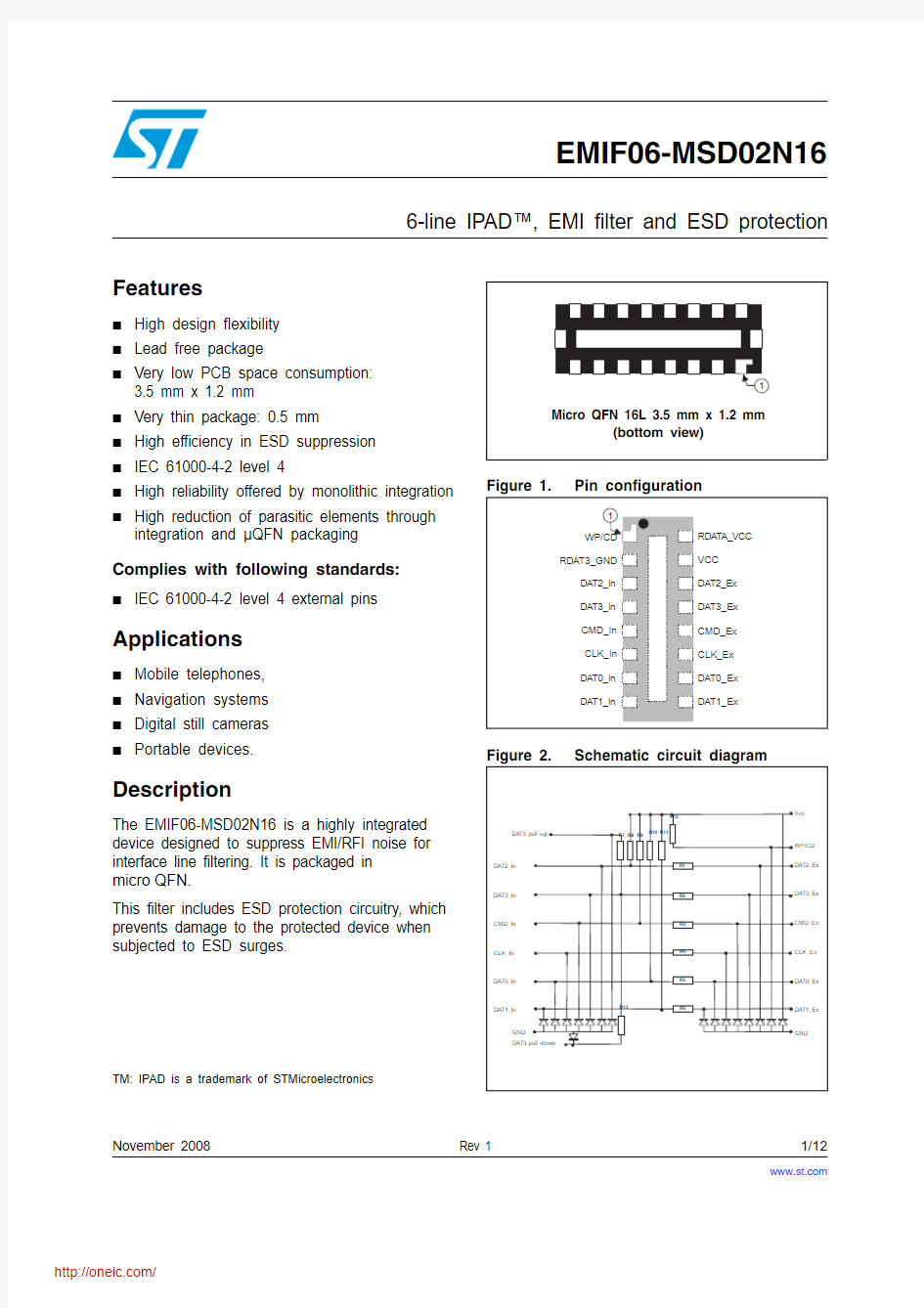
The EMIF06-MSD02N16 is a highly integrated device designed to suppress EMI/RFI noise for interface line filtering. It is packaged in micro QFN.
This filter includes ESD protection circuitry, which prevents damage to the protected device when subjected to ESD surges.
TM: IPAD is a trademark of STMicroelectronics
https://www.360docs.net/doc/0b19447266.html,
Characteristics EMIF06-MSD02N16
2/12
1 Characteristics
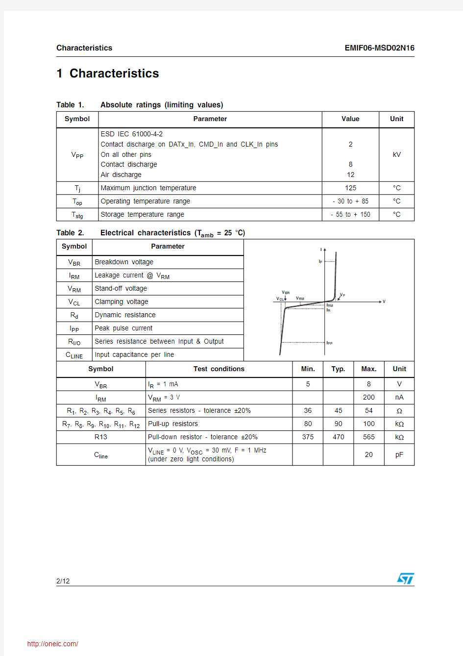
Table 1.
Absolute ratings (limiting values)
Symbol
Parameter
Value Unit
V PP
ESD IEC 61000-4-2
Contact discharge on DA Tx_In, CMD_In and CLK_In pins On all other pins Contact discharge Air discharge
2
812kV
T j Maximum junction temperature 125°C T op Operating temperature range - 30 to + 85°C T stg
Storage temperature range
- 55 to + 150
°C
EMIF06-MSD02N16
Characteristics
3/12
Figure 5.
ESD response to IEC 61000-4-2 (+12 kV air discharge) on one input (V in ) and on one output (V out )Figure 6.ESD response to IEC 61000-4-2 (-12 kV air discharge) on one input (V in ) and on one output (V out )
IN
OUT
55V Max
39V Max
IN
OUT
-41V Max
-34V Max
Application information EMIF06-MSD02N16
4/12
2 Application information
The EMIF06-mSD02N16 is a dedicated interface device for micro SD card/T -Flash card in
mobile phones. The device provides:
●ESD protection ●EMI filterering ●Pull-up resistors ●
Card detection circuit
2.1 ESD protection
Each pin is connected to a TVS diode able to withstand 12 kV on all pins except on
DATx_In, CMD_In and CLK_In.
2.2 EMI filtering
DATx, CMD and CLK lines are immunized against EMI radiations thanks to pi-filters. To
avoid any degradation of the signal integrity at high frequency, the total line capacitance stays lower than 20 pF making the device compatible with a clock frequency up to 52 MHz.
2.3 Pull-up resistors
As recommended by the SD Specifications (Part 1 Physical Layer Version 2.00), all the data
lines DATx and the CMD line must be pulled-up with resistors of 10 to 100 k Ω to avoid bus floating not only in SD 4-bit mode but also in SD 1-bit and SPI mode.
For the EMIF06-MSD02N16 device the pull-up resistor value has been fixed at 90 k Ω. This value makes the EMIF06-MSD02N16 compatible with most of the level shifters that may be used in the circuit including auto direction-sensing translators known to exhibit a weak current output.
2.4 Card detection circuit
The EMIF06-mSD02N16 provides the flexibility to use either mechanical card detection with
a dedicated pin connected to the memory card slot or the electrical card detection using the internal pull resistor of DAT3 of the micro SD card/T -Flash card.
In case of mechanical card detection, the user must add a pull-up on the circuit connected to the CD (Card Detect) of the micro-SD/T -Flash slot as shown in Figure 8.
EMIF06-MSD02N16
Application information
5/12
A pull-up of 90 k Ω is embedded into the EMIF06-MSD02N16. The routing corresponding to the mechanical card detection configuration is shown in Figure 9.Circuit routing for mechanical card detection
In case of electrical card detection, the user must add a pull-down on the circuit connected to the CD/DAT3 pin of the micro-SD/T -Flash pin as shown in Figure 10.Contact when
inserting the card
SD card
Pin 2–CD/DAT3Pin 3–CMD Pin 5–CLK Pin 6–GND Pin 7–DAT0Pin 8–DAT1
Pin 4Top level DAT3 pull-up
Card detect host input
Pin 2–Pin 3Pin 5Pin 6Pin 7Pin 4NC
HOST CONTROLLER
SD card
DAT3 (CD)
50 k Ω
GND
V DD
Ordering information scheme EMIF06-MSD02N16
6/12
A pull-down of 470k is embedded into the EMIF06-mSD02N16. The routing corresponding to the electrical card detection configuration is shown in the Figure 11. 3 Ordering information scheme
Pin 2Pin 2Pin 3Pin 5Pin 6Pin 4Top level
Pin 2DAT3 pull-down
Pin 2Pin 3Pin 5Pin 6Pin 7Pin 8
Pin 4
EMIF06-MSD02N16Package information
7/12
4 Package information
●
Epoxy meets UL94, V0
In order to meet environmental requirements, ST offers these devices in ECOP ACK ?
packages. These packages have a lead-free second level interconnect. The category of second level interconnect is marked on the inner box label, in compliance with JEDEC
Standard JESD97. The maximum ratings related to soldering conditions are also marked on the inner box label. ECOP ACK is an ST trademark. ECOPACK specifications are available at https://www.360docs.net/doc/0b19447266.html, .
Figure 13.Micro QFN 3.5x1.2 16L Figure 14.Marking
Package information EMIF06-MSD02N16
8/12
Note:Product marking may be rotated by 90° for assembly plant differentiation. In no case should this product marking be used to orient the component for its placement on a PCB. Only pin1
mark is to be used for this purpose.
EMIF06-MSD02N16Recommendation on PCB assembly
9/12
5
Recommendation on PCB assembly
5.1
Stencil opening design
1.
General recommendation on stencil opening design
a) Stencil opening dimensions: L (Length), W (Width), T (Thickness).
b) General design rule
Stencil thickness (T) = 75 ~ 125 μm
2. Reference design
a) Stencil opening thickness: 100 μm
b) Stencil opening for central exposed pad: Opening to footprint ratio is 50%.c)
Stencil opening for leads: Opening to footprint ratio is 90%.
Aspect Ratio W
T
----- 1.5≥=Aspect Area L W
×2T L W +()
---------------------------0.66
≥=
Recommendation on PCB assembly EMIF06-MSD02N16
10/12
5.2 Solder paste
1.Halide-free flux qualification ROL0 according to ANSI/J-STD-004.
2. “No clean” solder paste is recommended.
3. Offers a high tack force to resist component movement during high speed
4.
Solder paste with fine particles: powder particle size is 20-45 μm.
5.3 Placement
1.Manual positioning is not recommended.
2. It is recommended to use the lead recognition capabilities of the placement system, not
the outline centering
3. Standard tolerance of ± 0.05 mm is recommended.
4.
3.5 N placement force is recommended. Too much placement force can lead to
squeezed out solder paste and cause solder joints to short. Too low placement force can lead to insufficient contact between package and solder paste that could cause open solder joints or badly centered packages.
5. To improve the package placement accuracy, a bottom side optical control should be performed with a high resolution tool.
6.
For assembly, a perfect supporting of the PCB (all the more on flexible PCB) is recommended during solder paste printing, pick and place and reflow soldering by using optimized tools.
5.4 PCB design preference
1.To control the solder paste amount, the closed via is recommended instead of open
vias.
2.
The position of tracks and open vias in the solder area should be well balanced. The symmetrical layout is recommended, in case any tilt phenomena caused by asymmetrical solder paste amount due to the solder flow away.
分销商库存信息: STM
EMIF06-MSD02N16