GS72108AGTP-8I中文资料
GS72108ATP/J
256K x 8
2Mb Asynchronous SRAM
7, 8, 10, 12 ns
3.3 V V DD
Center V DD and V SS
SOJ, TSOP
Commercial Temp Industrial Temp Features
? Fast access time: 7, 8, 10, 12 ns
? CMOS low power operation: 135/115/95/80 mA at minimum cycle time
? Single 3.3 V power supply
? All inputs and outputs are TTL-compatible ? Fully static operation
? Industrial Temperature Option: –40° to 85°C ? Package line up
J: 400 mil, 36-pin SOJ package
TP: 400 mil, 44-pin TSOP Type II package
GP:Pb-free 400 mil, 44-pin TSOP Type II package ? Pb-Free TSOP-II package available
Description
The GS72108A is a high speed CMOS Static RAM organized as 262,144 words by 8 bits. Static design eliminates the need for external clocks or timing strobes. The GS operates on a single 3.3 V power supply and all inputs and outputs are TTL-compatible. The GS72108A is available in 400 mil SOJ and 400 mil TSOP Type-II packages.
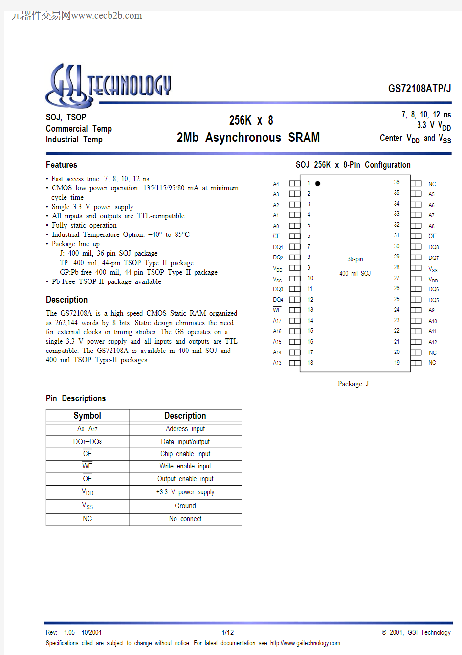
SOJ 256K x 8-Pin Configuration
Package J
Pin Descriptions
Symbol
Description
A 0–A 17Address input DQ 1–DQ 8
Data input/output CE Chip enable input WE Write enable input OE Output enable input V DD +3.3 V power supply
V SS Ground NC
No connect
3635343332313029282726252423222112345678910111213141516A 4A 3A 2A 1A 0CE DQ 1DQ 2V DD V SS DQ 3DQ 4WE A 17A 16A 15NC A 5A 6A 7A 8OE DQ 8DQ 7V SS V DD DQ 6DQ 5A 9A 10A 11A 1236-pin 400 mil SOJ
1718
A 14A 13
2019
NC
NC
GS72108ATP/J
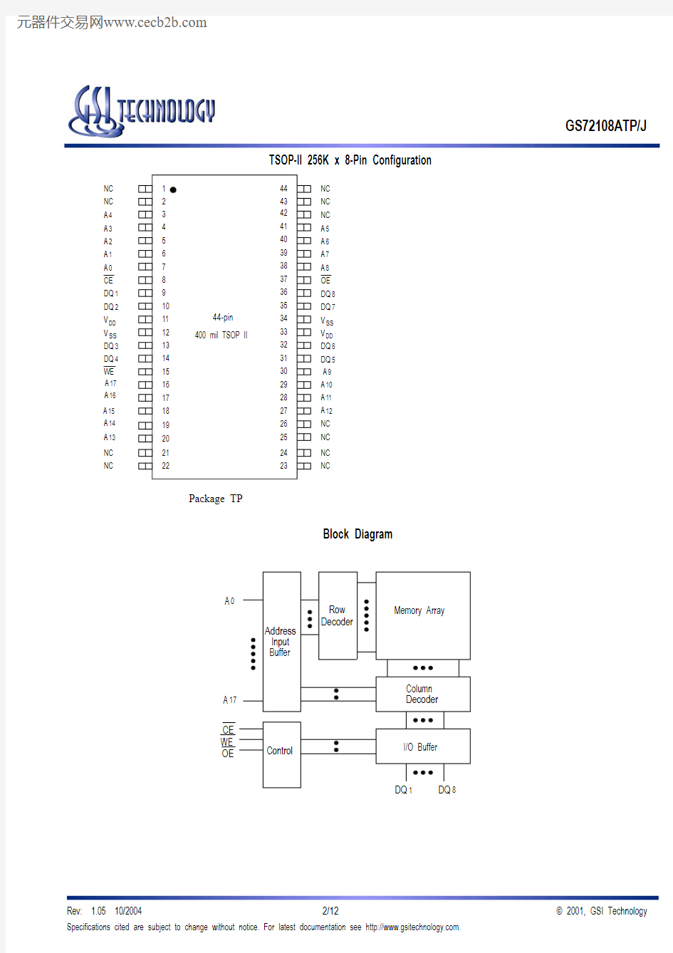
TSOP-II 256K x 8-Pin Configuration
Package TP
Block Diagram
424140393837363534333231302928273456789101112131415161718A 4A 3A 2A 1A 0CE DQ 1DQ 2V DD V SS DQ 3DQ 4WE NC A 5A 6A 7A 8OE DQ 8DQ 7V SS V DD DQ 6DQ 5A 10A 11A 12NC 44-pin 400 mil TSOP II
19202625NC 2122
NC NC
2423
NC NC
12NC NC 4443NC NC A 9A 13A 17A 16A 15A 14Memory Array
Row Decoder
Column Decoder
Address Input Buffer
Control
I/O Buffer
A 0
CE WE OE
DQ 1A 17DQ 8
GS72108ATP/J
Note:
X: “H” or “L”
Note:
Permanent device damage may occur if Absolute Maximum Ratings are exceeded. Functional operation shall be restricted to Recommended Operating Conditions. Exposure to higher than recommended voltages for extended periods of time could affect device reliability.
Truth Table
CE
OE
WE
DQ 1 to DQ 8
V DD Current
H X X Not Selected ISB 1, ISB 2
L L H Read I DD
L X L Write L H
H
High Z
Absolute Maximum Ratings
Parameter
Symbol
Rating
Unit
Supply Voltage V DD –0.5 to +4.6V Input Voltage V IN –0.5 to V DD +0.5
(≤ 4.6 V max.)V Output Voltage V OUT –0.5 to V DD +0.5(≤ 4.6 V max.)
V Allowable power dissipation PD 0.7W
Storage temperature
T STG
–55 to 150
o
C
GS72108ATP/J
Notes:
1.Input overshoot voltage should be less than V DD +2 V and not exceed 20 ns.
2.Input undershoot voltage should be greater than –2 V and not exceed 20 ns.
Notes:
1.Tested at T A = 25°C, f = 1 MHz
2.These parameters are sampled and are not 100% tested.
Recommended Operating Conditions
Parameter
Symbol
Min
Typ
Max
Unit
Supply Voltage for -7/-8/-10/-12
V DD 3.0 3.3 3.6V Input High Voltage V IH 2.0—V DD +0.3V Input Low Voltage V IL –0.3—0.8V
Ambient Temperature, Commercial Range T Ac 0—70o C Ambient Temperature,Industrial Range
T A I
–40
—
85
o
C
Capacitance
Parameter
Symbol
Test Condition
Max
Unit
Input Capacitance C IN V IN = 0 V 5pF Output Capacitance
C OUT
V OUT = 0 V
7
pF
DC I/O Pin Characteristics
Parameter
Symbol
Test Conditions
Min
Max
Input Leakage Current I IL V IN = 0 to V DD – 1 uA 1 uA Output Leakage
Current I LO Output High Z V OUT = 0 to V DD –1 uA 1 uA Output High Voltage V OH I OH = –4mA 2.4—Output Low Voltage
V OL
I LO = +4mA
—
0.4 V
GS72108ATP/J
AC Test Conditions
Power Supply Currents Parameter
Symbol
Test Conditions
0 to 70°C
–40 to 85°C 7 ns
8 ns
10 ns
12 ns
7 ns
8 ns
10 ns
12 ns
Operating Supply Current
I DD (max)CE ≤ V IL All other inputs ≥ V IH or ≤ V IL Min. cycle time I OUT = 0 mA 135 mA 115 mA 95 mA 80 mA 140 mA 120 mA 100 mA 85 mA
Standby Current
I SB1 (max)CE ≥ V IH All other inputs ≥ V IH or ≤V IL Min. cycle time 25 mA 20 mA 20 mA 15 mA 30 mA 25 mA 25 mA 20 mA
Standby Current
I SB2 (max)CE ≥ V DD - 0.2 V All other inputs ≥ V DD – 0.2 V or
≤ 0.2 V
5 mA 10 mA
DQ
VT = 1.4 V
50?30pF 1
DQ
3.3 V
Output Load 1
Output Load 2
589?434?
5pF 1
Notes:
1.Include scope and jig capacitance.
2.Test conditions as specified with output loading as shown in Fig. 1
unless otherwise noted.
3.Output load 2 for t LZ , t HZ , t OLZ and t OHZ
Parameter
Conditions
Input high level V IH = 2.4 V Input low level V IL = 0.4 V Input rise time tr = 1 V/ns Input fall time tf = 1 V/ns Input reference level 1.4 V Output reference level
1.4 V Output load
Fig. 1& 2
GS72108ATP/J
AC Characteristics * These parameters are sampled and are not 100% tested.
Read Cycle 1: CE = OE = V IL , WE = V IH
Read Cycle
Parameter Symbol -7-8
-10-12Unit Min Max Min Max Min Max Min Max Read cycle time t RC 7—8—10—12—ns Address access time t AA —7—8—10—12ns Chip enable access time (CE)t AC —7—8—10—12ns Byte enable access time (UB, LB)t AB —3— 3.5—4—5ns Output enable to output valid (OE)t OE —3— 3.5—4—5ns Output hold from address change t OH 3—3—3—3—ns Chip enable to output in low Z (CE)t LZ *3—3—3—3—ns Output enable to output in low Z (OE)t OLZ *0—0—0—0—ns Byte enable to output in low Z (UB, LB)t BLZ *0—0—0—0—ns Chip disable to output in High Z (CE)t HZ *— 3.5—4—5—6ns Output disable to output in High Z (OE)
t OHZ *
—
3
—
3.5
—4
—
5
ns
t AA
t OH
t RC
Address
Data Out
Previous Data
Data valid
GS72108ATP/J
Read Cycle 2: WE = V IH
* These parameters are sampled and are not 100% tested.
Write Cycle
Parameter Symbol -7-8-10
-12
Unit Min Max Min Max Min Max Min Max Write cycle time tWC 7—8—10—12—ns Address valid to end of write tAW 5— 5.5—7—8—ns Chip enable to end of write
tCW 5— 5.5—7—8—ns Data set up time tDW 3.5—4—5—6—ns Data hold time tDH 0—0—0—0—ns Write pulse width tWP 5— 5.5—7—8—ns Address set up time tAS 0—0—0—0—ns Write recovery time (WE)tWR 0—0—0—0—ns Write recovery time (CE)tWR10—0—0—0—ns Output Low Z from end of write tWLZ *3—3—3—3—ns Write to output in High Z
tWHZ *
—
3
—
3.5
—
4
—
5
ns
t AA
t RC
Address
t AC
t LZ
t OE
t OLZ
CE
OE
Data Out
t HZ
t OHZ
D ATA VALID
High impedance
GS72108ATP/J
Write Cycle 1: WE control
Write Cycle 2: CE control
t WC
Address
CE
WE
Data In
OE
Data Out
t AW
t CW
t AS
t WP
t WR
t DW
t DH
t WLZ
t WHZ
D ATA VALID
H IGH IMPEDANCE
t WC
Address
CE
WE
Data In
OE
Data Out
t AW
t WP
t AS
t CW
t WR1
t DW
t DH
D ATA VALID
H IGH IMPEDANCE
GS72108ATP/J
36-Pin SOJ, 400 mil
1
e
B1
D
A 1
A 2y
E H E
Q
c
L G E
Detail A
A
B A
Notes:
1.Dimension D& E do not include interlead flash.
2.Dimension B1 does not include dambar protrusion/intrusion.
3.Controlling dimension: inches
Symbol Dimension in inch
Dimension in mm min nom max min nom max A ——0.146—— 3.70A10.026——0.66——A20.1050.1100.115 2.67 2.80 2.92B 0.0130.0170.0210.330.430.53B1
0.0240.0280.0320.610.710.81c 0.0060.0080.0120.150.200.30D 0.9200.9240.92923.3723.4723.60E 0.3950.4000.40510.0410.1610.28e
—0.05—— 1.27—H E 0.4300.4350.44010.9311.0511.17G E 0.3540.3660.3789.009.309.60L 0.082—— 2.08——y ——0.004——0.10Q
0o
—
10o
0o
—
10o
GS72108ATP/J
44-Pin, 400 mil TSOP-II
D
12223
44
e
B
Q
A
A 1
A 2
y
c
Detail A
E
H E
L
L 1
A
Notes:
1.Dimension D& E do not include interlead flash.
2.Dimension B does not include dambar protrusion/intrusion.
3.Controlling dimension: mm
Symbol Dimension in inch
Dimension in mm min nom max min nom max A ——0.047—— 1.20A10.002——0.05——A20.0370.0390.0410.95 1.00 1.05B 0.010.0140.0180.250.350.45c —0.006——0.15—D 0.7210.7250.72918.3118.4118.51E 0.3960.4000.40410.0610.1610.26e
—0.031——0.80—H E 0.4550.4630.47111.5611.7611.96L 0.0160.0200.0240.400.500.60L1
—0.031——0.80—y ——0.004——0.10Q
0o
—
5o
0o
—
5o
GS72108ATP/J
*
Customers requiring delivery in Tape and Reel should add the character “T” to the end of the part number. For example: GS72108ATP-8T
Ordering Information
Part Number *
Package
Access Time
Temp. Range
Status
GS72108ATP-7400 mil TSOP-II 7 ns Commercial GS72108ATP-8400 mil TSOP-II 8 ns Commercial GS72108ATP-10400 mil TSOP-II 10 ns Commercial GS72108ATP-12400 mil TSOP-II 12 ns Commercial GS72108ATP78I 400 mil TSOP-II 7 ns Industrial GS72108ATP-8I 400 mil TSOP-II 8 ns Industrial GS72108ATP-10I 400 mil TSOP-II 10 ns Industrial GS72108ATP-12I 400 mil TSOP-II 12 ns Industrial GS72108AGP-7Pb-free 400 mil TSOP-II 7 ns Commercial GS72108AGP-8Pb-free 400 mil TSOP-II 8 ns Commercial GS72108AGP-10Pb-free 400 mil TSOP-II 10 ns Commercial GS72108AGP-12Pb-free 400 mil TSOP-II 12 ns Commercial GS72108AGP78I Pb-free 400 mil TSOP-II 7 ns Industrial GS72108AGTP-8I Pb-free 400 mil TSOP-II 8 ns Industrial GS72108AGP-10I Pb-free 400 mil TSOP-II 10 ns Industrial GS72108AGP-12I Pb-free 400 mil TSOP-II
12 ns Industrial GS72108AJ-7400 mil SOJ 7 ns Commercial GS72108AJ-8400 mil SOJ 8 ns Commercial GS72108AJ-10400 mil SOJ 10 ns Commercial GS72108AJ-12400 mil SOJ 12 ns Commercial GS72108AJ-7I 400 mil SOJ 7 ns Industrial GS72108AJ-8I 400 mil SOJ 8 ns Industrial GS72108AJ-10I 400 mil SOJ 10 ns Industrial GS72108AJ-12I
400 mil SOJ
12 ns
Industrial
GS72108ATP/J 2Mb Asynchronous Datasheet Revision History
Rev. Code: Old;
New Types of Changes
Format or Content
Page #/Revisions/Reason
72108A_r1 ? Creation of new datasheet
72108A_r1; 72108A_r1_01Content ? Added 6 ns speed bin ? Updated all power numbers
72108A_r1_01; 72108A_r1_02Content ? Updated Recommended Operating Conditions table on page 4? Changed FPBGA package from 6 x 10 to 6 x 8 (package U)
72108A_r1_02; 72108A_r1_03Content? Removed all references to “U” package
72108A_r1_03; 72108A_r1_04Content ? Removed 6 ns speed bin from entire document ? Added 7 ns speed bin to entire document
72108A_r1_04; 72108A_r1_05Content ? Updated format
? Added Pb-free information for TSOP-II package