AV102-12中文资料

HIP3? Variable Attenuator 1.70–2.00 GHz
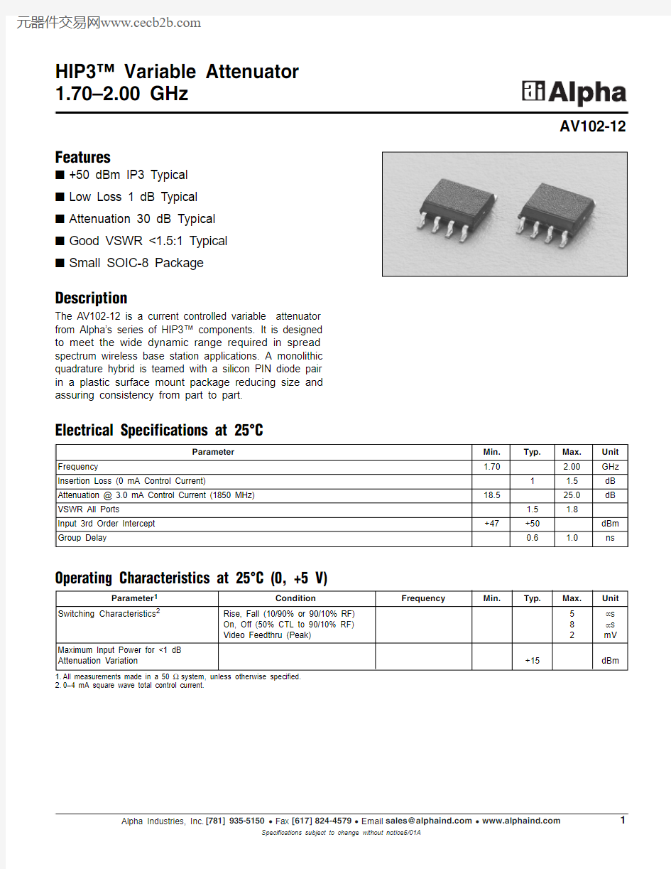
Features
I +50 dBm IP3 Typical I Low Loss 1 dB Typical I Attenuation 30 dB Typical I Good VSWR <1.5:1 Typical I Small SOIC-8 Package
AV102-12
Description
The AV102-12 is a current controlled variable attenuator from Alpha’s series of HIP3? components.It is designed to meet the wide dynamic range required in spread spectrum wireless base station applications.A monolithic quadrature hybrid is teamed with a silicon PIN diode pair in a plastic surface mount package reducing size and assuring consistency from part to part.
Electrical Specifications at 25°C
Parameter
1
Condition
Frequency
Min.
Typ.
Max.Unit Switching Characteristics 2
Rise, Fall (10/90% or 90/10% RF)5μs On, Off (50% CTL to 90/10% RF)8μs Video Feedthru (Peak)
2
mV Maximum Input Power for <1 dB Attenuation Variation
+15
dBm
Operating Characteristics at 25°C (0, +5 V)
1.All measurements made in a 50 ?system, unless otherwise specified.
2.0–4 mA square wave total control current.
V S W R (:1)
Input/Output VSWR vs. Current
@ 1700 MHz
1.0
1.1
1.21.31.41.50.0000
0.00100.00200.00300.00400.0050Current (Amps)Input
Output
V S W R (:1)
Input/Output VSWR vs. Current
@ 1850 MHz
1.0
1.1
1.21.31.4
1.5Current (Amps)0.0000
0.0010
0.0020
0.0030
0.0040
0.0050
Input
Output
A t t e n u a t i o n (d
B )
0.0000
0.00100.00200.00300.00400.0050
Attenuation vs. Current
-50.0
-40.0-30.0-20.0-10.0
0.0Current (Amps)
A t t e n u a t i o n (d
B )
1.70
1.80
1.90
2.00
Attenuation vs. Frequency
-25.0
-20.0
-15.0
-10.0-5.0
0.0Frequency (GHz)
0.0 mA 0.2 mA 0.7 mA
1.7 mA
2.4 mA
3.0 mA
Input/Output VSWR vs. Current
@ 2000 MHz
1.0
1.1
1.21.31.4
1.5Current (Amps)V S W R (:1)
0.0000
0.0010
0.0020
0.0030
0.0040
0.0050
Input Output
D i o d e C u r r e n t (m A )
4006008001000
Typical PIN Diode Current vs. Voltage
0.01
0.1
1
10
Diode Voltage (mV)
Typical Performance Data
Characteristic
Value
RF Input Power .5 W CW, 4 W @ 12.5%
Duty Cycle Control Current 50 mA Each Diode Operating Temperature -40 to +85°C Storage Temperature
-40 to +85°C
Maximum Reverse Diode Voltage -10 V Electrostatic Discharge
+125 V
Absolute Maximum Ratings
Note:Operating this device above any of these parameters may cause irreversible damage.
Recommended Board Layout
0.0190 TYP.
0.0555 TYP.
SOIC-8
0.049
0.016 MAX.
0.004 (0.10 mm)
0.007 (0.17 mm)
8?
PIN 1CONTROL CURRENT
GND
RF In
GND
GND RF Out
CONTROL CURRENT GND Pin Out
Connection Diagram
Material is 10 mil FR4.