MAX4124中文资料
General Description
The MAX4122–MAX4129 family of operational amplifiers combines wide bandwidth and excellent DC accuracy with Rail-to-Rail ?operation at the inputs and outputs. These devices require only 650μA per amplifier, and operate from either a single supply (+2.7V to +6.5V) or dual supplies (±1.35V to ±3.25V) with a common-mode voltage range that extends 250mV beyond V EE and V CC . They are capa-ble of driving 250?loads. The MAX4122/MAX4123/MAX4126/MAX4127/MAX4129 have a 5MHz gain band-width product, while the decompensated MAX4124/MAX4125/MAX4128 (stable at closed-looped gains of 10 or greater) have a 25MHz gain bandwidth product. In addition, the MAX4123/MAX4125/MAX4127 feature a shutdown mode in which the outputs are placed in a high-impedance state and the supply current is reduced to only 25μA per amplifier.
With their rail-to-rail input common-mode range and output swing, these amplifiers are ideal for low-voltage single-supply operation. Although the minimum operat-ing voltage is specified at 2.7V, the devices typically operate down to 1.8V. In addition, low offset voltage and high speed make them the ideal signal-condition-ing stages for precision, low-voltage, data-acquisition systems. The MAX4122 and MAX4124 come in the space-saving 5-pin SOT23-5 package.
________________________Applications
Battery-Powered Instruments Portable Equipment Data-Acquisition Systems Signal Conditioning
Low-Power, Low-Voltage Applications
Features
o 5-Pin SOT23 Package (MAX4122/4)o +2.7V to +6.5V Single-Supply Operation
o Rail-to-Rail Input Common-Mode Voltage Range o Rail-to-Rail Output Voltage Swing
o 5MHz Gain-Bandwidth Product (MAX4122/3/6/7/9)25MHz Gain-Bandwidth Product (MAX4124/5/8)o 650μA Quiescent Current per Amplifier o 25μA Shutdown Function (MAX4123/5/7)o 200μV Offset Voltage
o No Phase Reversal for Overdriven Inputs o Drive 250?Loads
o Stable with 500pF Capacitive Loads o Unity-Gain Stable (MAX4122/3/6/7/9)Stable at Gains ≥10V/V (MAX4124/5/8)
MAX4122–MAX4129
Single/Dual/Quad, Wide-Bandwidth, Low-Power,
Single-Supply Rail-to-Rail I/O Op Amps
________________________________________________________________Maxim Integrated Products
1
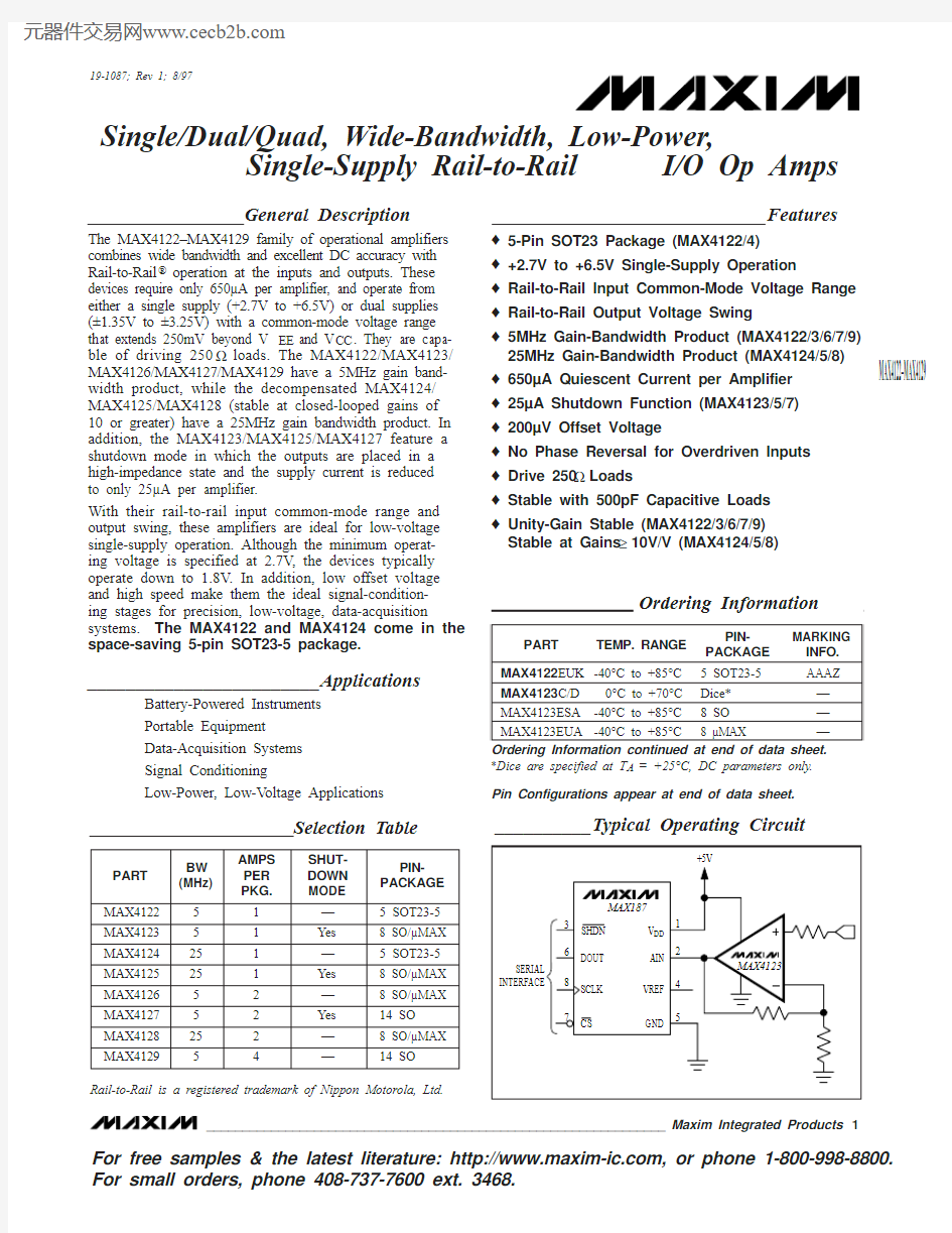
__________Typical Operating Circuit
19-1087; Rev 1; 8/97
Pin Configurations appear at end of data sheet.
For free samples & the latest literature: https://www.360docs.net/doc/2818440382.html,, or phone 1-800-998-8800.For small orders, phone 408-737-7600 ext. 3468.
Rail-to-Rail is a registered trademark of Nippon Motorola, Ltd.
M A X 4122–M A X 4129
Single-Supply Rail-to-Rail I/O Op Amps 2_______________________________________________________________________________________
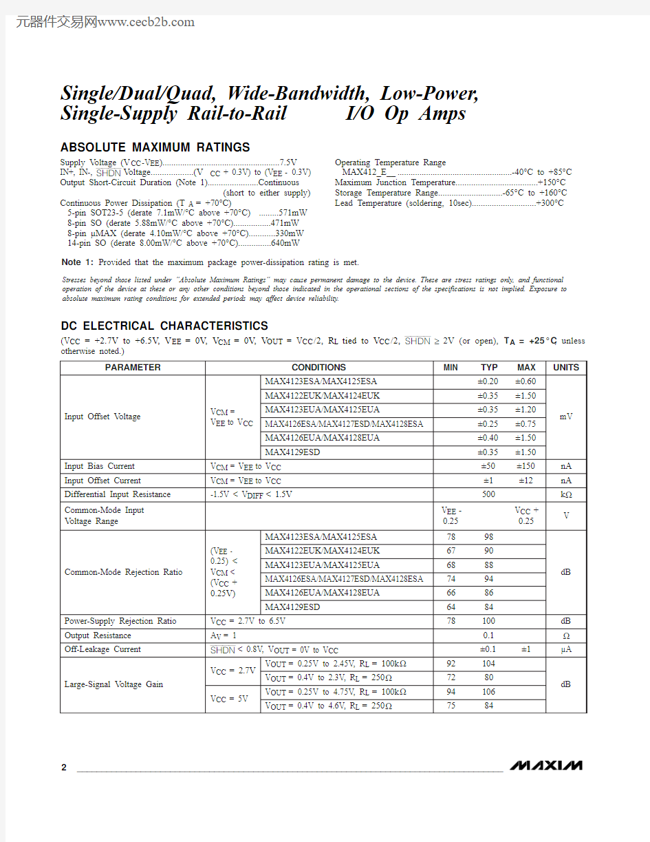
ABSOLUTE MAXIMUM RATINGS
DC ELECTRICAL CHARACTERISTICS
(V CC = +2.7V to +6.5V, V EE = 0V, V CM = 0V, V OUT = V CC /2, R L tied to V CC /2, SHDN ≥2V (or open), T A = +25°C , unless otherwise noted.)
Stresses beyond those listed under “Absolute Maximum Ratings” may cause permanent damage to the device. These are stress ratings only, and functional operation of the device at these or any other conditions beyond those indicated in the operational sections of the specifications is not implied. Exposure to absolute maximum rating conditions for extended periods may affect device reliability.
Supply Voltage (V CC -V EE ).....................................................7.5V IN+, IN-, SHDN Voltage...................(V CC + 0.3V) to (V EE - 0.3V)Output Short-Circuit Duration (Note 1).......................Continuous
(short to either supply)
Continuous Power Dissipation (T A = +70°C)
5-pin SOT23-5 (derate 7.1mW/°C above +70°C).........571mW 8-pin SO (derate 5.88mW/°C above +70°C).................471mW 8-pin μMAX (derate 4.10mW/°C above +70°C)............330mW 14-pin SO (derate 8.00mW/°C above +70°C)...............640mW
Operating Temperature Range
MAX412_E__....................................................-40°C to +85°C Maximum Junction Temperature.....................................+150°C Storage Temperature Range.............................-65°C to +160°C Lead Temperature (soldering, 10sec).............................+300°C
Note 1:Provided that the maximum package power-dissipation rating is met.
MAX4122–MAX4129
Single-Supply Rail-to-Rail I/O Op Amps
DC ELECTRICAL CHARACTERISTICS
(V CC = +2.7V to +6.5V, V EE = 0V, V CM = 0V, V OUT = V CC /2, R L tied to V CC /2, SHDN ≥2V (or open), T A = -40°C to +85°C , unless otherwise noted.)
DC ELECTRICAL CHARACTERISTICS (continued)
(V CC = +2.7V to +6.5V, V EE = 0V, V CM = 0V, V OUT = V CC /2, R L tied to V CC /2, SHDN ≥2V (or open), T A = +25°C , unless otherwise noted.)
M A X 4122–M A X 4129
Single-Supply Rail-to-Rail I/O Op Amps
DC ELECTRICAL CHARACTERISTICS (continued)
(V CC = +2.7V to +6.5V, V EE = 0V, V CM = 0V, V OUT = V CC /2, R L tied to V CC /2, SHDN ≥2V (or open), T A = -40°C to +85°C , unless otherwise noted.)
AC ELECTRICAL CHARACTERISTICS
(V CC = +2.7V to +6.5V, V EE = 0V, SHDN ≥2V (or open), T A = +25°C , unless otherwise noted.)
MAX4122–MAX4129
Single-Supply Rail-to-Rail I/O Op Amps
_______________________________________________________________________________________5
60
-40100
1k
10k
1M
10M
100k
100M
MAX4322/26/29
GAIN AND PHASE vs. FREQUENCY
-20FREQUENCY (Hz)
G A I N (d B )
020
40
P H A S E (D E G R E E S )
180144
720-72
-144
-180-108-3636108
60
-40100
1k
10k
1M
10M
100k
100M
MAX4122/23/26/27/29
GAIN AND PHASE vs. FREQUENCY
(WITH C LOAD )
-20
FREQUENCY (Hz)G A I N (d B )
20
40
P H A S E (D E G R E E S )180
144
720
-72-144
-180-108-3636108
0-100
10
1001k 100k 1M 10M 10k 100M
MAX4122/23/26/27/29POWER-SUPPLY REJECTION
vs. FREQUENCY
-80
FREQUENCY (Hz)
P S R (d B )
-60-40-20__________________________________________Typical Operating Characteristics
(V CC = +5V, V EE = 0V, V CM = V CC /2, T A = +25°C, unless otherwise noted.)
AC ELECTRICAL CHARACTERISTICS (continued)
(V CC = +2.7V to +6.5V, V EE = 0V, SHDN ≥2V (or open), T A = +25°C , unless otherwise noted.)
60
-40100
1k
10k
100k
1M
10M
MAX4124/25/28
GAIN AND PHASE vs. FREQUENCY
-20
FREQUENCY (Hz)
G A I N (d B )
P H A S E (D E G R E E S )0
20
40180144
-180
-144
-108-72
-36360
10872
60
-40100
1k
10k
1M
10M
100k
100M
MAX4124/25/28
GAIN AND PHASE vs. FREQUENCY
(WITH C LOAD )-20
FREQUENCY (Hz)G A I N (d B )
20
40P H A S E (D E G R E E
S )180
144720-72
-144
-180-108-3636108
0-100
10
1001k 100k 1M 10M 10k 100M
MAX4124/25/28
POWER-SUPPLY REJECTION
vs. FREQUENCY
-80FREQUENCY (Hz)
P S R (d B )
-60-40-20
Typical Operating Characteristics (continued)
(V CC = +5V, V EE = 0V, V CM = V CC /2, T A = +25°C, unless otherwise noted.)
M A X 4122–M A X 4129
Single-Supply Rail-to-Rail I/O Op Amps 6_______________________________________________________________________________________
1k
10k 10M
FREQUENCY (Hz)
100k 1M
100
1305060708090100110120MAX4126/27/28/29
CHANNEL SEPARATION vs. FREQUENCY
M A X 4122/29-07
C H A N N E L S E P A R A T I O N (d B )
100
0.01
100
1k
100k
1M
10M
10k
100M
MAX4122/23/26/27/29OUTPUT IMPEDANCE vs. FREQUENCY
0.1
FREQUENCY (Hz)
O U T P U T I M P E D A N C E (?)
1
10
100
0.1
100
1k
100k
1M
10M
10k
100M
MAX4124/25/28OUTPUT IMPEDANCE vs. FREQUENCY
FREQUENCY (Hz)
O U T P U T I M P E D A N C E (?)
1
10
900500
550600650700750800850-40-25-10
5
20
35
50
65
8095SUPPLY CURRENT PER AMPLIFIER
vs. TEMPERATURE
TEMPERATURE (°C)S
U P P L Y C U R R E N T (μA )
10
2030405060-40-25-105203550658095
MAX4323/MAX4327SHUTDOWN SUPPLY CURRENT
vs. TEMPERATURE
TEMPERATURE (°C)S H U T D O W N S U P P L Y C U R R E N T (m A
)
-10
-505101520-40-25-10
5
20
35
50
65
80
95
OUTPUT LEAKAGE CURRENT
vs. TEMPERATURE
TEMPERATURE (°C)
L E A K A G E C U R R E N T (μA
)
-3.00
-2.25-0.75-1.5001.500.752.253.00-40-25-10
5
20
35
50
65
80
95INPUT OFFSET VOLTAGE vs. TEMPERATURE
TEMPERATURE (°C)V O L T A G E (
m V )
-50
0123456
INPUT BIAS CURRENT vs. COMMON-MODE VOLTAGE
COMMON-MODE VOLTAGE (V)I N P U T B I A S C U R R E N T (n A )
-40-30-20-10010203040
50-60
-50-40-25-10
5
20
35
50
65
80
95
INPUT BIAS CURRENT vs. TEMPERATURE
TEMPERATURE (°C)
I N P U T B I A S C U R R E N T (n A )
-40-30-20-1001020304050
Typical Operating Characteristics (continued)
(V CC = +5V, V EE = 0V, V CM = V CC /2, T A = +25°C, unless otherwise noted.)
MAX4122–MAX4129
Single-Supply Rail-to-Rail I/O Op Amps
_______________________________________________________________________________________7
12080
859095100105110115-40-25-10
5
20
35
50
65
80
95
COMMON-MODE REJECTION
vs. TEMPERATURE
TEMPERATURE (°C)
C O M M O N -M O
D
E R E J E C T I O N (d B )
12060
600
110OUTPUT VOLTAGE: EITHER SUPPLY (mV)
G A I N (
d B )
300
908070100
200
500
100400
LARGE-SIGNAL GAIN vs. OUTPUT VOLTAGE
2500
-40-25-10
5
20
35
50
65
80
95
MINIMUM OUTPUT VOLTAGE
vs. TEMPERATURE
50200
TEMPERATURE (°C)
V O U T - V E E (m V )
150
100
50100150200250300
-40-25-10
5
20
35
50
65
80
95
MAXIMUM OUTPUT VOLTAGE
vs. TEMPERATURE
TEMPERATURE (°C)
V C C - V O U T (m V )
12060
600
110OUTPUT VOLTAGE: EITHER SUPPLY (mV)
G A I N (d B )
300
9080
70100
200
500
100400
LARGE-SIGNAL GAIN vs. OUTPUT VOLTAGE
125
75
-40-25-10
5
20
35
50
65
80
95
LARGE-SIGNAL GAIN vs. TEMPERATURE
85115
TEMPERATURE (°C)
G A I N (d B )
1059580
90120110100
12060
600
110G A I N (d B )
300908070100200500100400LARGE-SIGNAL GAIN vs. OUTPUT VOLTAGE
OUTPUT VOLTAGE: EITHER SUPPLY (mV)
12060
600
110G A I N (d B )
300
90
8070100
200
500
100
400
LARGE-SIGNAL GAIN vs. OUTPUT VOLTAGE
OUTPUT VOLTAGE: EITHER SUPPLY (mV)
125
75
-40-25-10
5
20
35
50
65
80
95
LARGE-SIGNAL GAIN
vs. TEMPERATURE
85115TEMPERATURE (°C)
G A I N (d B )
1059580
90120110100
Typical Operating Characteristics (continued)
(V CC = +5V, V EE = 0V, V CM = V CC /2, T A = +25°C, unless otherwise noted.)
M A X 4122–M A X 4129
Single-Supply Rail-to-Rail I/O Op Amps 8_______________________________________________________________________________________
IN (5mV/div)TIME (200ns/div)OUT (50mV/div)A V = +10
MAX4124/25/28
SMALL-SIGNAL TRANSIENT RESPONSE (NONINVERTING)
M A X 4122/29-31
IN (5mV/div)
TIME (200ns/div)
OUT (50mV/div)
A V = -10
MAX4124/25/28
SMALL-SIGNAL TRANSIENT RESPONSE (INVERTING)
M A X 4122/29-32
IN (2V/div)
TIME (2μs/div)
OUT (2V/div)
A V = -1
MAX4122/23/26/27/29LARGE-SIGNAL TRANSIENT RESPONSE (INVERTING)
M A X 4122/29-34
1.2
1.31.51.41.61.71.81.9-40-25-10
5
20
35
50
65
80
95MAX4123
MINIMUM OPERATING VOLTAGE
vs. TEMPERATURE
M A X 4122/29-25
TEMPERATURE (°C)M I N I M U M O P E R A T I N G V O L T A G E (V )
IN
TIME (200ns/div)
V O L T A G E (50m V /d i v )
OUT A V = +1
MAX4122/23/26/27/29SMALL-SIGNAL TRANSIENT RESPONSE (NONINVERTING)
M A X 4122/29-28
10
100k
10k FREQUENCY (Hz)
100
1k 0.0400
0.005
0.0100.0150.0200.0250.0300.035MAX4122/23/26/27/29 TOTAL HARMONIC DISTORTION AND NOISE vs. FREQUENCY
T H D & N O I S E (%)
0.1
0.001
4.0
4.4
4.2
5.0
4.84.6MAX4123
TOTAL HARMONIC DISTORTION AND NOISE vs. PEAK-TO-PEAK SIGNAL AMPLITUDE
PEAK-TO-PEAK SIGNAL AMPLITUDE (V)
T H D + N (%)
0.01
IN
TIME (200ns/div)V O L T A G E (50m V /d i v )
OUT
A V = -1
MAX4122/23/26/27/29SMALL-SIGNAL TRANSIENT RESPONSE (INVERTING)
M A X 4122/29-29
IN
TIME (2μs/div)
V O L T A G E (2V /d i v )
OUT
A V = +1
MAX4122/23/26/27/29LARGE-SIGNAL TRANSIENT RESPONSE (NONINVERTING)
M A X 4122/29-30
Typical Operating Characteristics (continued)
(V CC = +5V, V EE = 0V, V CM = V CC /2, T A = +25°C, unless otherwise noted.)
MAX4122–MAX4129
Single-Supply Rail-to-Rail I/O Op Amps
_______________________________________________________________________________________9
IN
(200mV/div)
TIME (2μs/div)
OUT (2V/div)
A V = +10
MAX4124/25/28
LARGE-SIGNAL TRANSIENT RESPONSE (NONINVERTING)
M A X 4122/29-33
IN
(200mV/div)
TIME (2μs/div)
OUT (2V/div)
A V = -10
MAX4124/25/28
LARGE-SIGNAL TRANSIENT RESPONSE (INVERTING)
M A X 4122/29-35
Pin Description
M A X 4122–M A X 4129
Single-Supply Rail-to-Rail I/O Op Amps 10______________________________________________________________________________________
Figure 2. Input Protection Circuit
Figure 1a. Reducing Offset Error Due to Bias Current
(Noninverting)Figure 1b. Reducing Offset Error Due to Bias Current (Inverting)
Applications Information
Rail-to-Rail Input Stage
Devices in the MAX4122–MAX4129 family of high-speed amplifiers have rail-to-rail input and output stages designed for low-voltage single-supply opera-tion. The input stage consists of separate NPN and PNP differential stages, which combine to provide an input common-mode range extending 0.2V beyond the supply rails. The PNP stage is active for input voltages close to the negative rail, and the NPN stage is active for input voltages near the positive rail. The input offset voltage is typically below 200μV. The switchover transi-tion region, which occurs near V CC /2, has been extended to minimize the slight degradation in CMRR caused by the mismatch of the input pairs. Their low offset voltage, high bandwidth, and rail-to-rail common-mode range make these op amps excellent choices for precision low-voltage data-acquisition systems.
Since the input stage switches between the NPN and PNP pairs, the input bias current changes polarity as the input voltage passes through the transition region.To reduce the offset error caused by input bias cur-rents flowing through external source impedances,match the effective impedance seen by each input (Figures 1a, 1b). High source impedances, together with the input capacitance, can create a parasitic pole that produces an underdamped signal response.Reducing the input impedance or placing a small (2pF to 10pF) capacitor across the feedback resistor improves the response.
The MAX4122–MAX4129’s inputs are protected from large differential input voltages by 1k ?series resistors and back-to-back triple diodes across the inputs (Figure 2). For differential input voltages less than 1.8V the input resistance is typically 500k ?. For differential input voltages greater than 1.8V the input resistance is approximately 2k ?, and the input bias current is
Rail-to-Rail Output Stage
The minimum output voltage will be within millivolts of ground for single-supply operation where the load is referenced to ground (V EE ). Figure 3 shows the input voltage range and output voltage swing of a MAX4123connected as a voltage follower. With a +3V supply and the load tied to ground, the output swings from
0.00V to 2.90V. The maximum output voltage swing depends on the load, but will be within 150mV of a +3V supply, even with the maximum load (500?to ground).Driving a capacitive load can cause instability in most high-speed op amps, especially those with low quiescent current. The MAX4122–MAX4129 have a high tolerance for capacitive loads. They are stable with capacitive loads up to 500pF. Figure 4 gives the stable operating region for capacitive loads. Figures 5–8 show the response with capacitive loads, and the results of adding an isolation resistor in series with the output (Figure 9).The resistor improves the circuit’s phase margin by iso-lating the load capacitor from the op amp’s output.
MAX4122–MAX4129
Single-Supply Rail-to-Rail I/O Op Amps
______________________________________________________________________________________11
IN
TIME (2μs/div)
OUT
V CC = 3V A V = +1
Figure 3. Rail-to-Rail Input /Output Voltage Range
10,000
100
100
1k
10k
RESISTIVE LOAD (?)
1000
UNSTABLE REGION
R L TO V EE V OUT = V CC /2
Figure 4. Capacitive-Load Stability
M A X 4122–M A X 4129
Single-Supply Rail-to-Rail I/O Op Amps 12
______________________________________________________________________________________
IN
V O L T A G E (50m V /d i v )
OUT
A V = +1C L = 500pF
Figure 5. MAX4122/23/26/27/29 Small-Signal Transient Response with Capacitive Load IN
TIME (400ns/div)V O L T A G E (50m V /d i v )
OUT
A V = +1C L = 1000pF R S = 39?
Figure 7. MAX4122/23/26/27/29 Transient Response to Capacitive Load with Isolation Resistor
IN V O L T A G E
OUT A V = +10C L = 500pF
(5mV/div)
(50mV/div)
Figure 6. MAX4124/25/28 Small-Signal Transient Response with Capacitive Load
IN
V O L T A G E
OUT A V = +10C L = 1000pF R S = 56?
(5mV/div)(50mV/div)
Figure 8. MAX4124/25/28 Transient Response to Capacitive Load with Isolation Resistor
Figure 9. Capacitive-Load-Driving Circuit Figure 10. Power-Up/Shutdown Test Circuit
MAX4122–MAX4129
Single-Supply Rail-to-Rail I/O Op Amps
______________________________________________________________________________________13
V CC TIME (5μs/div)
V O L T A G E (1V /d i v )
OUT
Figure 11. Power-Up Output Voltage SHDN (1V/div )
TIME (2μs/div)OUT
(0.5V/div)V CC = 2.7V R L = 10k ?
Figure 13. Shutdown Output Voltage V CC (1V/div)
TIME (5μs/div)
I CC
(500μA/div)
Figure 12. Power-Up Supply Current
SHDN (1V/div)
TIME (2μs/div)
I CC
(500μA/div)
V CC = 2.7V
Figure 14. Shutdown Enable/Disable Supply Current
Power-Up and Shutdown Mode
The MAX4122–MAX4129 amplifiers typically settle with-in 1μs after power-up. Using the test circuit of Figure 10, Figures 11 and 12 show the output voltage and supply current on power-up.
The MAX4123, MAX4125, and MAX4127 have a shut-down option. When the shutdown pin (SHDN ) is pulled low, the supply current drops below 25μA per amplifier and the amplifiers are disabled with the outputs in a high-impedance state. Pulling SHDN high or leaving it floating enables the amplifier. In the dual-amplifier MAX4129, the shutdown functions operate indepen-dently. Figures 13 and 14 show the output voltage and supply current responses of the MAX4123 to a shut-down pulse.
Power Supplies and Layout
The MAX4122–MAX4129 operate from a single +2.7V to +6.5V power supply, or from dual supplies of ±1.35V to ±3.25V. For single-supply operation, bypass the power supply with a 0.1μF ceramic capacitor in parallel with at least 1μF. For dual supplies, bypass each sup-ply to ground.
Good layout improves performance by decreasing the amount of stray capacitance at the op amp’s inputs and outputs. To decrease stray capacitance, minimize trace lengths and resistor leads by placing external components close to the op amp’s pins.
M A X 4122–M A X 4129
Single-Supply Rail-to-Rail I/O Op Amps 14______________________________________________________________________________________
Pin Configurations
MAX4122–MAX4129
Single-Supply Rail-to-Rail I/O Op Amps
______________________________________________________________________________________
15
__________________________________________________________Chip Topographies
OUT2
IN2-
IN2+
0.066"(1.676mm)0.053"(1.346mm)
V CC SHDN1
SHDN2V EE
V CC
OUT1
V CC
IN1- IN1+
V EE
SHDN
V CC
0.055"(1.397mm)
0.036"(0.914mm)
OUT V EE
IN-iN+
V EE
TRANSISTOR COUNT: 170SUBSTRATE CONNECTED TO V EE
TRANSISTOR COUNT: 340SUBSTRATE CONNECTED TO V EE
MAX4123/MAX4125
MAX4127/MAX4128
Ordering Information (continued)
*Dice are specified at T A = +25°C, DC parameters only.
M A X 4122–M A X 4129
Single-Supply Rail-to-Rail I/O Op Amps ________________________________________________________Package Information
Maxim cannot assume responsibility for use of any circuitry other than circuitry entirely embodied in a Maxim product. No circuit patent licenses are implied. Maxim reserves the right to change the circuitry and specifications without notice at any time.
16____________________Maxim Integrated Products, 120 San Gabriel Drive, Sunnyvale, CA 94086 408-737-7600?1997 Maxim Integrated Products
Printed USA
is a registered trademark of Maxim Integrated Products.