50N06中文资料
UNISONIC TECHNOLOGIES CO., LTD
50N06
MOSFET
50 Amps, 60 Volts
N-CHANNEL POWER MOSFET
DESCRIPTION
The UTC 50N06 is three-terminal silicon device with current conduction capability of about 50A, fast switching speed. Low on-state resistance, breakdown voltage rating of 60V, and max threshold voltages of 4 volt.
It is mainly suitable electronic ballast, and low power switching mode power appliances.
FEATURES
* R DS(ON) = 23m ?@V GS = 10 V
* Ultra low gate charge ( typical 30 nC )
* Low reverse transfer Capacitance ( C RSS = typical 80 pF ) * Fast switching capability
* 100% avalanche energy specified * Improved dv/dt capability
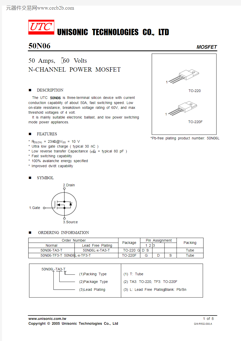
SYMBOL
1.Gate
TO-220
1
1
TO-220F
*Pb-free plating product number: 50N06L
ORDERING INFORMATION
Order Number Pin Assignment
Normal
Lead Free Plating Package 1 2 3 Packing
50N06-TA3-T 50N06L-x-TA3-T TO-220 G D S Tube 50N06-TF3-T 50N06L-x-TF3-T TO-220F G D S Tube
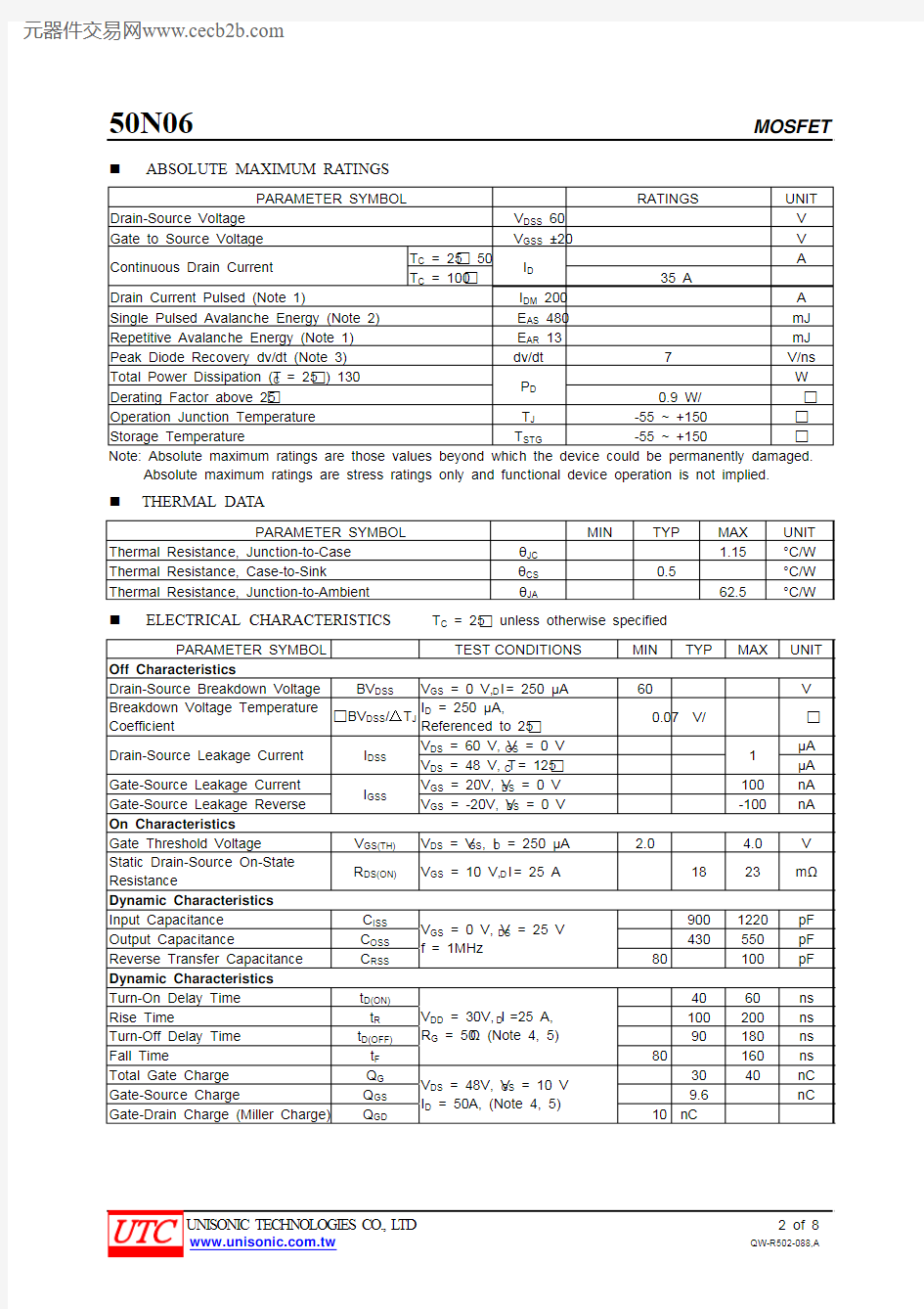
ABSOLUTE MAXIMUM RATINGS
PARAMETER SYMBOL RATINGS UNIT
Drain-Source Voltage V DSS 60 V Gate to Source Voltage V GSS ±20 V
T C = 25 50 A
Continuous Drain Current T C = 100 I D
35 A
Drain Current Pulsed (Note 1) I DM 200 A Single Pulsed Avalanche Energy (Note 2) E AS 480 mJ Repetitive Avalanche Energy (Note 1) E AR 13 mJ Peak Diode Recovery dv/dt (Note 3) dv/dt 7 V/ns
Total Power Dissipation (T C = 25 ) 130 W
Derating Factor above 25
P D
0.9 W/ Operation Junction Temperature T J -55 ~ +150 Storage Temperature T STG -55 ~ +150 Note: Absolute maximum ratings are those values beyond which the device could be permanently damaged.
Absolute maximum ratings are stress ratings only and functional device operation is not implied.
THERMAL DATA
PARAMETER SYMBOL MIN TYP MAX UNIT
Thermal Resistance, Junction-to-Case θJC 1.15 °C/W Thermal Resistance, Case-to-Sink θCS 0.5 °C/W Thermal Resistance, Junction-to-Ambient θJA 62.5 °C/W
ELECTRICAL CHARACTERISTICS T C = 25 unless otherwise specified
PARAMETER SYMBOL TEST CONDITIONS MIN TYP MAX UNIT Off Characteristics
Drain-Source Breakdown Voltage BV DSS V GS = 0 V, I D = 250 μA 60 V Breakdown Voltage Temperature Coefficient BV DSS /△T J I D = 250 μA,
Referenced to 25
0.07 V/
V DS = 60 V, V GS = 0 V μA
Drain-Source Leakage Current I DSS
V DS = 48 V, T C = 125
1 μA Gate-Source Leakage Current V GS = 20V, V DS = 0 V 100 nA
Gate-Source Leakage Reverse I GSS
V GS = -20V, V DS = 0 V -100 nA On Characteristics Gate Threshold Voltage V GS(TH) V DS = V GS , I D = 250 μA 2.0 4.0 V Static Drain-Source On-State
Resistance
R DS(ON) V GS = 10 V, I D = 25 A 18 23 m ?
Dynamic Characteristics Input Capacitance C ISS 900 1220 pF
Output Capacitance C OSS 430 550 pF
Reverse Transfer Capacitance C RSS
V GS = 0 V, V DS = 25 V
f = 1MHz
80 100 pF Dynamic Characteristics Turn-On Delay Time t D(ON) 40 60 ns
Rise Time t R 100 200 ns Turn-Off Delay Time t D(OFF) 90 180 ns
Fall Time t F V DD = 30V, I D =25 A, R G = 50? (Note 4, 5) 80 160 ns Total Gate Charge Q G 30 40 nC
Gate-Source Charge Q GS 9.6 nC
Gate-Drain Charge (Miller Charge) Q GD V DS = 48V, V GS = 10 V
I D = 50A, (Note 4, 5)
10 nC
2. L=5.6mH, I AS=50A, V DD=25V, R G=0?, Starting T J=25
3. I SD≤50A, di/dt≤300A/μs, V DD≤BV DSS, Starting T J=25
4. Pulse Test: Pulse Width≤300μs,Duty Cycle≤2%
5. Essentially independent of operating temperature.
TEST CIRCUITS AND WAVEFORMS
V DD
V GS (Driver)
I SD (D.U.T.)
Body Diode
Forward Voltage Drop
V DS
(D.U.T.)
Fig. 1A Peak Diode Recovery dv/dt Test Circuit
Fig. 1B Peak Diode Recovery dv/dt Waveforms
TEST CIRCUITS AND WAVEFORMS (Cont.)
R L
DD
V DS
90%
10%
V GS
t
Fig. 2A Switching Test Circuit Fig. 2B Switching Waveforms
Fig. 3A Gate Charge Test Circuit
Fig. 3B Gate Charge Waveform
10V
L
V DD
I AS
Fig. 4A Unclamped Inductive Switching Test Circuit Fig. 4B Unclamped Inductive Switching Waveforms
TYPICAL CHARACTERISTICS
10
1010101010Drain -Source Voltage , V DS (V)
D r a i n C u r r e n t , I D (A )
On-State Characteristics
101010Gate-Source Voltage , V GS (V)
D r a i n C u r r e n t , I D (A )
Transfer Characteristics
0D r a i n -S o u r c e O n -R e s i s t a n c e , R D S (O N ) (m Ω)
Drain Current , I D (A)
4080200
100140On-Resistance Variation vs . Drain Current
102
10100
0.2Source-Drain Voltage , V SD (V)
R e v e r s e D r a i n C u r r e n t , I S D (A )
On State Current vs. Allowable Case
Temperature
1.6
0.40.60.8 1.0 1.2 1.4
2060120160180
5
Drain -Source Voltage, V DC (V)
C a p a c i t a n c e (p F )
Capacitance Characteristics
1020G a t e -t o -S o u r c e V o l t a g e , V G S (V )
Total Gate Charge , Q G (nC)
81012Gate Charge Characteristics
6
4015253035
TYPICAL CHARACTERISTICS(Cont.)
-100D r a i n -S o u r c e B r e a k d o w n V o l t a g e , B V D S S (N o r m a l i z e d )
Junction Temperature , T J (℃)
-50
50
200
100
150Breakdown Voltage Variation vs . Junction
, -5050100150On-Resistance Variation vs . 0Junction Temperature , T J (℃)
10
1010
Drain-Source Voltage , V DS (V)
D r a i n C u r r e n t , I D ,(A )
Maximum Safe Operating
1010D r a i n C u r r e n t , I D (A )
Case Temperature, T C (℃)
7510050Maximum Drain Current vs . Case Temperature 0
125502510203040101010
10
10Square Wave Pulse Duration , t 1 (sec)
T h e r m a l R e s p o n s e , Z θJ C (t )
10
101010
10101010101Transient Thermal