1.5KA15中文资料
Notes:(1) Non-repetitive current pulse, per Fig.3 and derated above T A = 25°C per Fig.2
(2) Mounted on copper pad area of 1.6 x 1.6”(40 x 40mm)per Fig.5
(3) 8.3ms single half sine-wave or equivalent square wave, duty cycle = 4 pulses per minutes maximum
Document Number https://www.360docs.net/doc/3f8667196.html,
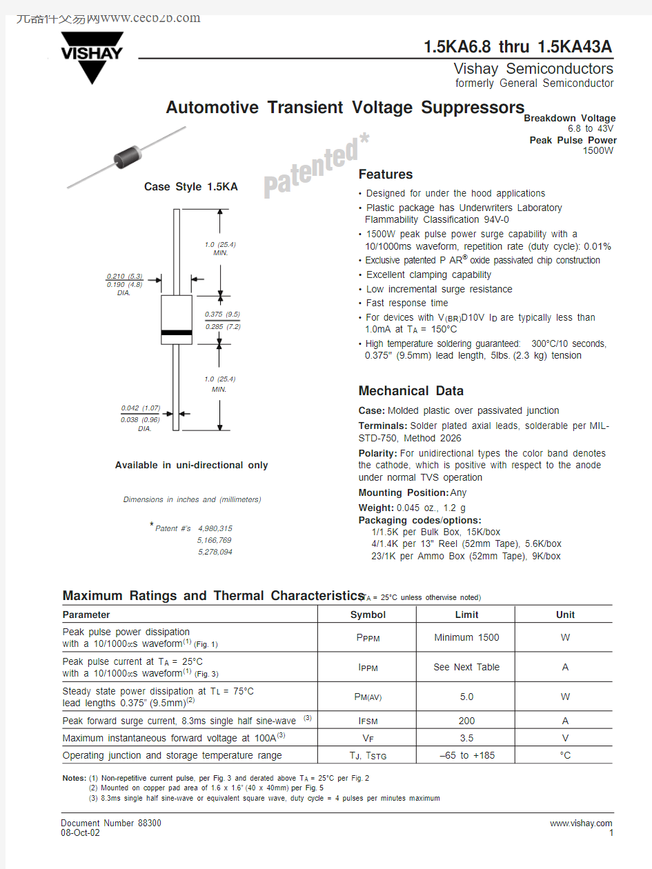
1.5KA6.8 thru 1.5KA43A
Vishay Semiconductors
formerly General Semiconductor
https://www.360docs.net/doc/3f8667196.html, Document Number 88300
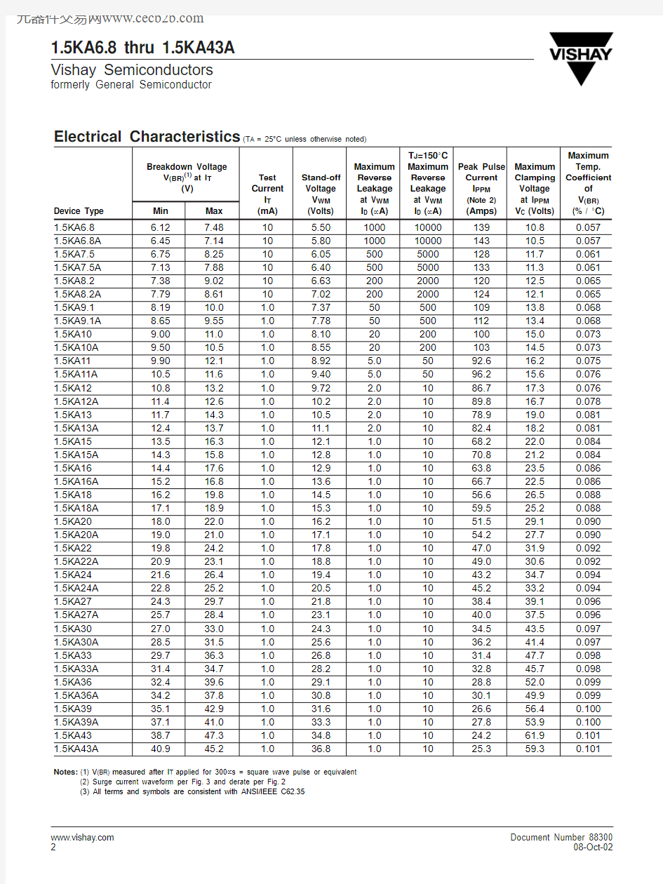
Electrical Characteristics (T
A
= 25°C unless otherwise noted)
T J =150°C Maximum Breakdown Voltage
Maximum Maximum Peak Pulse Maximum Temp.V (BR)(1)at I T
Test Stand-off Reverse Reverse Current Clamping Coefficient
(V)
Current Voltage Leakage Leakage I PPM
Voltage of I T V WM at V WM at V WM (Note 2)
at l PPM V (BR)Device Type
Min
Max
(mA)(Volts)
I D (μA)
I D (μA)
(Amps)
V C (Volts)
(% / °C)
1.5KA6.8 6.127.4810 5.5010001000013910.80.0571.5KA6.8A 6.457.1410 5.8010001000014310.50.0571.5KA7.5 6.758.2510 6.05500500012811.70.0611.5KA7.5A 7.137.8810 6.40500500013311.30.0611.5KA8.27.389.0210 6.6320020001201
2.50.0651.5KA8.2A 7.798.61107.02200200012412.10.0651.5KA9.18.1910.0 1.07.37505001091
3.80.0681.5KA9.1A 8.659.55 1.07.785050011213.40.0681.5KA109.0011.0 1.08.102020010015.00.0731.5KA10A 9.5010.5 1.08.55202001031
4.50.0731.5KA119.9012.1 1.08.92
5.05092.61
6.20.0751.5KA11A 10.511.6 1.09.40 5.05096.215.60.0761.5KA1210.813.2 1.09.72 2.01086.71
7.30.0761.5KA12A 11.412.6 1.010.2 2.01089.816.70.0781.5KA1311.714.3 1.010.5 2.0107
8.91
9.00.0811.5KA13A 12.413.7 1.011.1 2.01082.418.20.0811.5KA1513.516.3 1.012.1 1.01068.222.00.0841.5KA15A 14.315.8 1.012.8 1.01070.821.20.0841.5KA1614.417.6 1.012.9 1.01063.823.50.0861.5KA16A 15.216.8 1.013.6 1.01066.722.50.0861.5KA1816.219.8 1.014.5 1.01056.626.50.0881.5KA18A 17.118.9 1.015.3 1.01059.525.20.0881.5KA2018.022.0 1.016.2 1.01051.529.10.0901.5KA20A 19.021.0 1.017.1 1.01054.227.70.0901.5KA2219.824.2 1.017.8 1.01047.031.90.0921.5KA22A 20.923.1 1.018.8 1.01049.030.60.0921.5KA2421.626.4 1.019.4 1.01043.234.70.0941.5KA24A 22.825.2 1.020.5 1.01045.233.20.0941.5KA2724.329.7 1.021.8 1.01038.439.10.0961.5KA27A 25.728.4 1.023.1 1.01040.037.50.0961.5KA3027.033.0 1.024.3 1.01034.543.50.0971.5KA30A 28.531.5 1.025.6 1.01036.241.40.0971.5KA3329.736.3 1.026.8 1.01031.447.70.0981.5KA33A 31.434.7 1.028.2 1.01032.845.70.0981.5KA3632.439.6 1.029.1 1.01028.852.00.0991.5KA36A 34.237.8 1.030.8 1.01030.149.90.0991.5KA3935.142.9 1.031.6 1.01026.656.40.1001.5KA39A 37.141.0 1.033.3 1.01027.853.90.1001.5KA4338.747.3 1.034.8 1.01024.261.90.1011.5KA43A 40.945.2 1.036.8 1.01025.359.30.101
Notes:(1) V (BR)measured after I T applied for 300μs = square wave pulse or equivalent
(2) Surge current waveform per Fig.3 and derate per Fig.2
(3) All terms and symbols are consistent with ANSI/IEEE C62.35
1.5KA6.8 thru 1.5KA43A
Vishay Semiconductors
formerly General Semiconductor
Document Number https://www.360docs.net/doc/3f8667196.html,
Ratings and
Characteristic Curves (T A = 25°C unless otherwise noted)
1
10
100
Fig. 2 – Pulse Derating Curve
P P P M — P e a k P u l s e P o w e r (k W )
Fig. 1 – Peak Pulse Power Rating Curve
Number of Cycles at 60H Z
P M (A V ), S t e a d y S t a t e P o w e r D i s s i p a t i o n (W )
T L — Lead Temperature (°C)
I P P M — P e a k P u l s e C u r r e n t , % I R S M