CST仿真色散图流程
One of the most important reports in metamaterial topics is “Dispersion curve”, which determines the band-gap behavior of the band-gap structures. In this article two examples that could clearly show the right way of getting this report including two extra Matlab code scripts, are presented.
I hope this article could be helpful for the students who are love Electromagnetic !
“Thanks to Dr Miguel Navarro -Cía Imperial College London for his valuable comment”.
Dispersion Diagram Example 1: Slow Wave Helix General Description
This example demonstrates an eigenmode calculation using periodic boundaries in z-direction and a very meaningful example for showing how we can get the dispersion diagram in CST MWS for periodic structures. This example already is available in example folder of CST MWS in path of:
“C:\Program Files (x86)\CST STUDIO SUITE 2013\Examples\MWS\Eigenmode\TET\Slow Wave\helix.cst ”
Structure description:
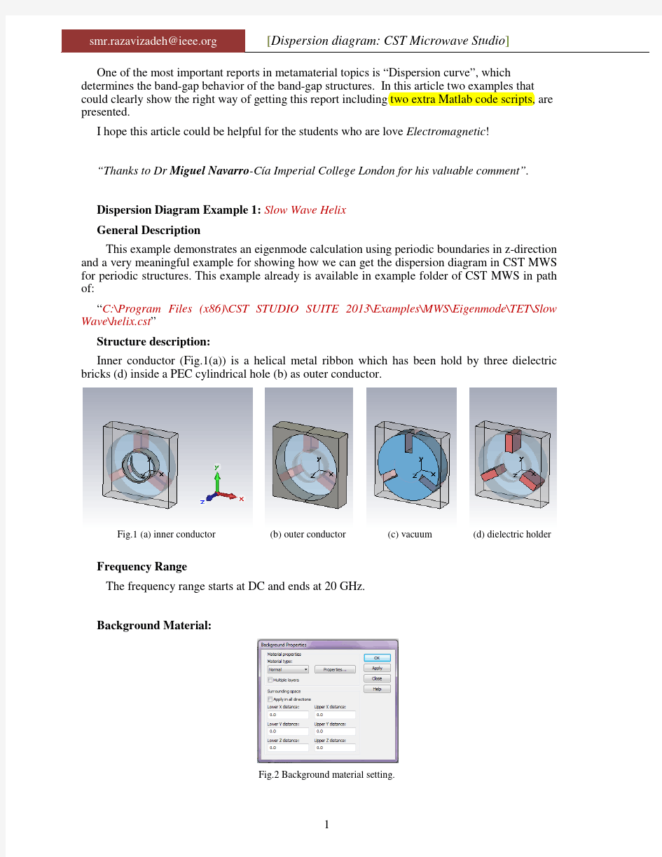
Inner conductor (Fig.1(a)) is a helical metal ribbon which has been hold by three dielectric bricks (d) inside a PEC cylindrical hole (b) as outer conductor.
Fig.1 (a) inner conductor
(b) outer conductor
(c) vacuum
(d) dielectric holder
Frequency Range
The frequency range starts at DC and ends at 20 GHz.
Background Material:
Fig.2 Background material setting.
第一个例子
Mesh setting:
Click on the objects in navigation tree and R. Click on the object; then choose the “Local mesh properties” and set it as the following suggestions:
Vacuum: Meshgroup1
The automesh option is disabled for the two inlets which are not parallel to the coordinate axes. Other elements: Meshgroup2 The automesh option is enabled. (Inner&outer conductor, holders)
Fig.3 mesh setting of the model components.
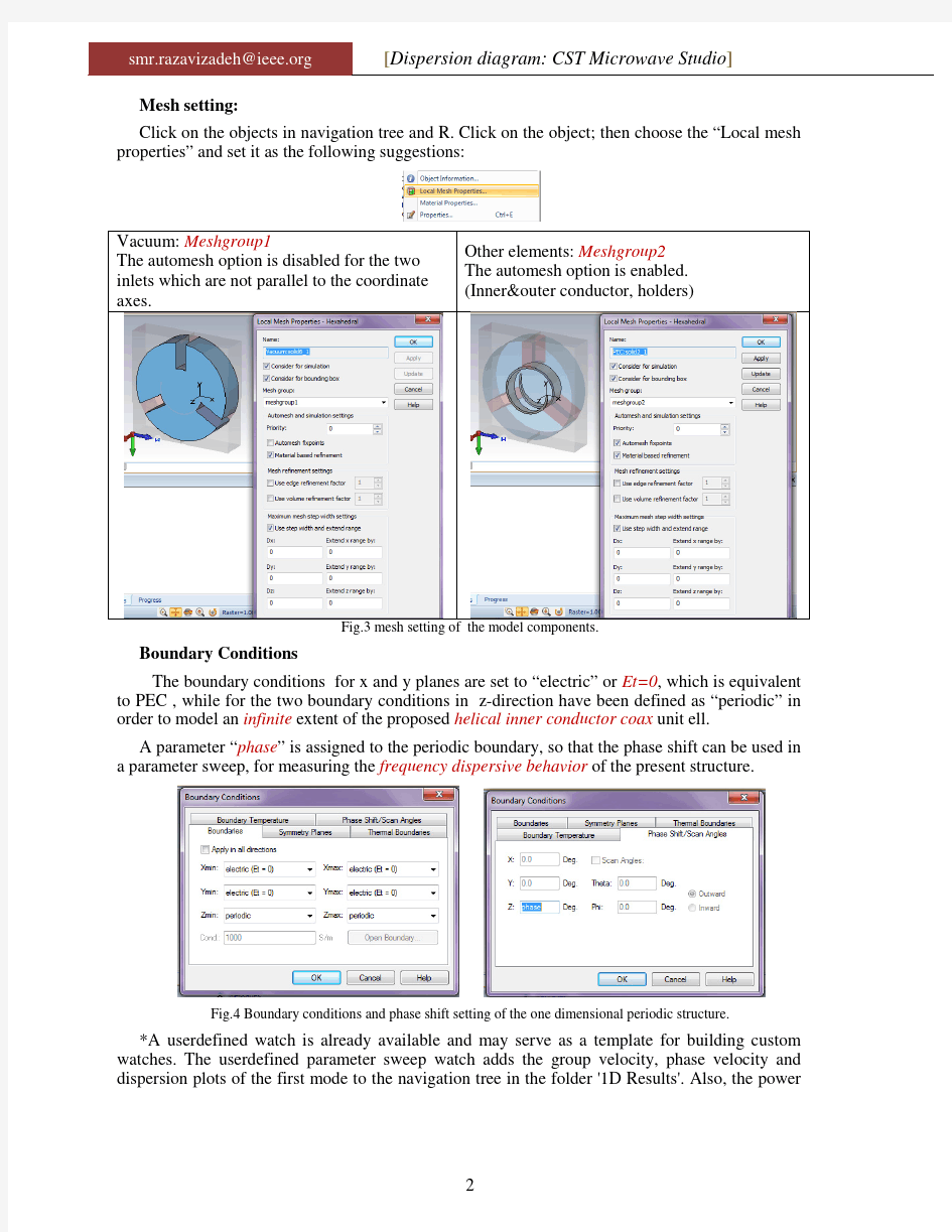
Boundary Conditions
The boundary conditions for x and y planes are set to “electric” or Et=0, which is equivalent to PEC , while for the two boundary conditions in z-direction have been defined as “periodic” in order to model an infinite extent of the proposed helical inner conductor coax unit ell.
A parameter “phase” is assigned to the periodic boundary, so that the phase shift can be used in a parameter sweep, for measuring the frequency dispersive behavior of the present structure.
Fig.4 Boundary conditions and phase shift setting of the one dimensional periodic structure.
*A userdefined watch is already available and may serve as a template for building custom watches. The userdefined parameter sweep watch adds the group velocity, phase velocity and dispersion plots of the first mode to the navigation tree in the folder '1D Results'. Also, the power
flow and Pierce Impedance can be seen in the folder '1D Results'. In parameter sweep window, select "Edit" to view or modify the source code.
>
Fig.5 the user-defined VBA codes of the important reports of the simulation as dispersion
curve, phase & group velocity and Pierce impedance.
But I preferred that the following method for setting the dispersion diagram.
Post Processing:
The dispersion diagram, which is a graph based on “frequency” vs. spatial phase variations of the predefined parameter of “phase”, could obtained by the following step by step process:
1)Recall the TBP and choose the “2D and 3D Field Results>3D Eigenmode Result”
Fig.6 the outline of defining the postprocessing setup of dispersion plot in CST
MWS.
2)For obtaining the dispersion data of the modes start one by one from the first mode, then
after finishing simulation operation export the data in “txt” format(available in “Table”
folder in Navigation tree) for our future postprocessing in Matlab environment.
3)Evaluate
Solver Setup
Whenever the “Eigenmode Solver” is started, a specific number of the lowest resonance frequencies of the structure are calculated. Since only the fundamental mode is of interest, the number of modes is reduced to “1”, and the JDM eigenmode solver is chosen, which is faster for the given example.
Fig.7 Eigenmode Solver setting for calculating the dispersion characteristics of the proposed
periodic structure.
After the parameter sweep has been selected from the Eigenmode Solver's dialog, a new sequence is added, and the parameter "phase" is chosen to be swept from 0 to 180 degrees in 19 steps for an equal steps.
Fig.8 Parametric sweep setup for phase shift parameter of “phase” in the space periodicity
direction.
Start:
If you set lower sweep limit at zero, the machine temporary would interrupt the process and alert we the parameter is zero, don’t care about it and click Ok to continue the operation.
>>
Fig.10
Results
During the run process the real time dispersion results is accessible from the Table folder, as a plot based on frequency vs. phase parameter, as following:
(a)
(b)
Fig. 11 The dispersion diagram based on (a) TBP result template, and (b) VBA
userdefined.
As shown in Fig. 11, all the data are the same but in Fig.11(a) the horizontal axis is the phase.
Export the data of the Mode “1”
>>
>>
Fig. 12 extraction of table dispersion data
Open via excel
Open a new Excel file and open from it your txt file of “Mode1.txt”:
>
>
>>
Fig. 13 The preparation of the dispersion text data file for producing the
compatible *.csv file
We should keep just the phase and value column and eliminate others, then edit the title of the value column as “Frequency(Mode1)”, finally save as a CSV file format, as shown in Fig. 13. We should repeat the simulation for remained modes frequencies as presented in Fig. 14, and extract the favorite data for updating the previous “mode1.csv” data file.
Fig. 15 How we can update the calculation for the higher mode?
Fig. 16 all the dispersion data gathered in one csv file for plotting the final
dispersion diagram for first forth modes of the proposed 1D-periodic structure.
Mtalab Code for plotting the dispersion diagram
For publishing all of your plot result, especially in IEEE publications, we should import our data into Matlab environment, as a perfect engineering tool to sketch various plots in a unique plot in a high resolution view. Here we present a brief quick guide about it.
1)Run Matlab
2) import the dispersion CSV file.
>
4)disable the header and text box.
>>
5)Run the plot m.file(see the appendix)
Final result:
Fig. the final sketch of the dispersion diagram obtained by a MATLAB plotting
program (Appendix).
Phase(Deg)
F r e q u e n c y (
G
H z )
Example2. 2D-periodic structure dispersion diagram
In this section, dispersion characterization of surface waves propagating on a mushroom-like periodic structure is investigated using CST MWS. Mushroom-like EBG structures
Wavenumber k is an important parameter to describe the propagation property of electromagnetic waves. In a lossless case , the phase constant is β = k .
Usually, β is a function of frequency ω. Once the phase constant is obtained, the phase velocity (v p) and group velocity (v g) can be derived:
??=
?
?
??? ??=
????
(2-1)
Furthermore, the field distribution can also be determined, such as the field variation in a
transverse direction. For a plane wave in free space, the relation between β and ω is a linear function:
????=?= ??????
(2-2)
For surface waves propagating in an EBG structure, it is usually difficult to give an explicit expression for the wavenumber k . One has to either solve an eigen-value equation or perform a full wave simulation to determine the wavenumber. It is important to point out that the solution of an eigen-value equation may not be unique.
In another words, there may exist several different propagation constants at the same frequency. Each one is known as a specific mode with its own phase velocity, group velocity, and field distribution. The relation between β and ω is often plotted out and referred to as the dispersion diagram .
For a periodic structure such as the EBG, the field distribution of a surface wave is also periodic with a proper phase delay determined by the wavenumber ? ???β? and periodicity p . Thus, each surface wave mode can be decomposed into an infinite series of space harmonic waves.
?????,?,??=∑??????,???
??β?? ????? , β????? = β? ??? + ? (2-3)
Here, we assume the periodic and propagation direction is the x direction. Although these space
harmonics have different phase velocities, they share the same group velocity. Furthermore, these space harmonics cannot exist individually because each single harmonic does not satisfy the boundary conditions of the periodic structure. Only their summation satisfies the boundary conditions. Thus, they are considered to be the same mode.
Another important observation from (2-3) is that the dispersion curve β? ??? is periodic along the β- axis with a periodicity of 2π/p. Therefore, we only need to plot the dispersion relation within one single period, namely, 0 ≤ β?? ≤ 2?/??, which is known as the Brillouin zone. This concept can be easily extended to two-dimensional periodic structures, where the Brillouin zone becomes a two-dimensional square area:
0 ≤ β?? ≤ 2?/?? , 0 ≤ β?? ≤ 2?/??
Figure 2-1 shows the dispersion diagram of the mushroom-like EBG structure.
The vertical axis shows the frequency and the horizontal axis represents the
values of the transverse wavenumbers (βx, βy). Three specific points are: Γ, X
and M.
Let us consider a plane wave impinging on a periodic surface. For surface waves, the angle of incidence is equal to 90° (parallel with the surface). For this value, the wave propagation on a periodic structure cannot be investigated using the plane wave response. The exact position of pass bands and band gaps in the frequency spectrum can be obtained only by the dispersion relation of surface waves (i.e. calculating the resonant frequencies of eigenmodes) along the contour of the irreducible Brillouin zone.
Brillouin Zone in CST Microwave Studio
In dispersion diagram of a 2D-periodic structure, we are faced with an special definition of the frequency dispersion effects of the surface wave phase variations in three main directions usually labeled as Γ to X, X to M and M to Γ, which we know as “Brillouin Zone”, as shown in Fig..
Fig.2-2. Brillouin zone definition of a 2D-periodic structure (in a full period of
p x=p y=d, we have 2π radian phase change).
Now we should describe three directions phase constant variations with a 2D-plot. In this plot the independent variable of β-axis is a set of ordered pairs of:
??????_?
?????_?
Then, the first set has been called as “Γ to X”:
??????_?:0 ?? 180 ???.
?????_?=0
And the second set, “X to M”:
??????_?=180 ???.
?????_?: 0 ?? 180 ???
Finally, the last set is “M to Γ”:
??????_?:0 ?? 180 ???.
?????_?:0 ?? 180 ???;"???? ??? ????????? ???????? ??? ????????"
Fig.2-3. example of “dispersion diagram” of a 2D-periodic structure, based on
Brillouin Zone definition (in this example the step of sweep is 30deg).
This simulator uses finite integration technique (FIT). The unit cell of the structure under investigation has to be drawn with periodic boundary conditions applied in the appropriate directions. The phase shift is changed along the boundary of the irreducible Brillouin zone and frequencies of eigenmodes are obtained in each step. Because of slow-wave behavior of surface
waves, dispersion curves are calculated only in the region under the light line, as shown in Fig.
2.1. Band gaps occur in frequency intervals, where no dispersion curves in the slow-wave region are present.
Model and Dimension
The most popular mushroom-like EBG structure which is used here as an example of 2D-periodic structures, is composed of a grounded FR4 substrate with periodic square patch above, which the middle of the patch is connected with a via to the ground plane.
Parameter List of our example:
Substrate:(xs,ys) 15×15mm2, FR4(εr=4.5, loss tan. 0.025,
h s=1.6mm)
Patch size: (xs-gap, ys-gap) 14×14mm2 gap=1mm,
Via: radius Rp=0.5mm
Conductor: PEC, thickness(tm):0.035mm
Fig.2-4.
Fig. 2.5 shows the unit cell setup of a periodic structure with the proposed mushroom-like square lattice, for dispersion analysis in CST MWS. The main difference between the computational models in CST MWS and HFSS consists in the following fact. HFSS uses a perfectly matched layer (PML) to represent an infinite air layer above the unit cell, while in CST MWS, open boundaries are not allowed in combination with periodic walls, but only perfect electric conductor (PEC) or perfect magnetic conductor (PMC) boundary conditions can be applied.
(a)
(b)
Fig.2-5. The setup of (a) Background material and (b) six boundaries of the unit cell.
The Eigenmode Solver of CST Microwave Studio does not support open boundaries. In this case, the boundary condition of side walls of the unit cell can be considered periodic.
After many computer simulations with this program and comparing the obtained results with analytical and experimental considerations, a practical rule for the correct surface wave dispersion diagram computation was stated for background material and boundary setting.
Therefore, the key parameter in the computer model is then the height of the air space above of the dielectric substrate to emulate the free space over the structure (in “Background Setting” this space is “Upper Z-distance”), an airbox with the height of about many times of the dielectric slab thickness has to be placed over the unit cell. Based on numerous computer simulations and by comparing the obtained results with analytical and experimental considerations, the correct choice of approximately ten times the substrate thickness was established, “Upper Z-distance ?10·hs”[1].
The boundaries at the top and the bottom of the model should be defined as electric conductor or PEC (Et=0).
If the EBG surfaces are used as ground plane of antenna, like monopole this Figure 3(b) shows the frequency response of transmission coefficient S21, both TM and TE surface waves measured by using a pair of small monopole antennas oriented normally (TM mode) and parallel (TE mode) to the EBG surface.
Frequency Setting: 0-8GHz
Mesh setting:
For not complicated structures like this poject mesh setting is not required but if you want more and more precise results you can pay time for more dense mesh size!
Phase Shift Setting
“Phase_x” and “phase_y” are the phase variation of the slow surface wave on the periodic structure, in x- and y-directions, respectively. We know those parameters have a obvious relation with correspondent wave numbers as the following:
?????_?≡???????? ??????????? ????? ??? x-axis
?????_?≡?????
?????_?≡???????? ??????????? ????? ??? x-axis
?????_?≡?????
For symmetry with respect to the x- and y-axis’s, we define both of xs and ys with a new parameter of “d”.
Γ to X plot:
Sweep the “phase_x (βx d)” from 0 t0 180, with sample: 19 and “phase_y (βy d)=0”
X to M plot:
Sweep the “phase_y (βy d)” from 0 t0 180, with sample: 19 and “phase_x (βx d)=180”
Eigenmode Solver Setting
Start:
Don’t care about alert zero value for phase_x parameter.
Γ to X plot:
Sweep the “phase_x (βx d)” from 0t0 180, with sample: 19and “phase_y (βy d)=0” , the simulation takes not much more time, about 25 minutes by a typical laptop.
The figure shows phase variation linearity below 2.2GHz for Mode#1 and for surface wave propagation phase constant with respect to x-direction.
Export the data and save as “Mode1_Gamma2X.txt”:
The last value of phase_x is 180, that’s perfect! So go to Eigenmode>para sweep and delete phase_x and define phase_y from 0 to 180, then open “Result Template…” and do “Evaluate” for reset for new plot, “X to M”, then click the “Start”:
During the new parameter simulation, still the previous plot would be shown, don’t care about it! The real time new results are available in table format:
Updating the phase_y sweep data:
Recall the table plot, set the phase_y as, “abscissa” and phase_x at 180 as fixed x direction phase which is required for X to M plot,
It’s obvious that the upper limit of Frequency Band Gap region is about 2.13GHz.
Export:
Nav. Tree>R.Click on Table and choose the table. Then change phase_x t0 180 and apply, finally export:
>>
M to Γ Plot:
For convenience to extract this step data we first clean all the stored data of previous sweep by drawing for example a Brick then apply it to message of deletion would be shown, click Ok. In the next step delete that object and now the project is free of any data.
The last plot of Brillouin zone is based on diagonal propagation phase shift which is equivalent to k x=k y or phase_x=phase_y. So we can satisfy this by setting value of phase_y with phase_x, in parameters list window.
>>
Now recall Eigenmode solver and sweep par. And delete the phase_y and define phae_x: 180 to 0deg, with 19 samples, this constraint the calculations performed with descent variation, which is required for M to Γ plot.
Start the Sweep!
Results:
Export the results of the last parametric calculations as “M2Gamma_Mode1.txt”.
Preparing the final Dispersion diagram CSV file
In this section we should create the CSV file format of three correspondent text files of Γto X, X to M and M to Γ, respectively.
Γto X X to M M to Γ
In this step we should prepared a new excel book which contains in a serial format all the three calculated data set, compatible with the Brillouin zone definition, as following:
(a)
(b)
For plotting the desirable Brillouin zone diagram with MATLAB, We insert a new sequential numbering column, as shown in Fig. (b). It is important to determine boarder row numbers of the CSV data file, this issue has shown in the following table.
Plot Name Row range in main CSV data file
Γ to X 1-19 X to M 19-38 M to Γ
38-57
CST使用教程
1.1 软件介绍 CST公司总部位于德国达姆施塔特市,成立于1992年。它是一家专业电磁场仿真软件的提供商。CST软件采用有限积分法(Finite Integration)。其主要软件产品有: CST微波工作室—— 三维无源高频电磁场仿真软件包(S参量和天线) CST设计工作室—— 微波网络(有源及无源)仿真软件平台(微波放大器、混频器、谐波分析等) CST电磁工作室—— 三维静场及慢变场仿真软件包(电磁铁、变压器、交流接触器等)马飞亚(MAFIA)—— 通用大型全频段、二维及三维电磁场仿真软件包(包含静电场、准静场、简谐场、本振场、瞬态场、带电粒子与电磁场的自恰相互作用、热动力学场等模块) 在此,我们主要讨论“CST微波工作室”,它是一款无源微波器件及天线仿真软件,可以仿真耦合器、滤波器、环流器、隔离器、谐振腔、平面结构、连接器、电磁兼容、IC封装及各类天线和天线阵列,能够给出S参量、天线方向图等结果。 1.2 软件的基本操作 1.2.1 软件界面 启动软件后,可以看到如下窗口:
1.2.2 用户界面介绍
1.2.3 基本操作 1).模板的选择 CST MWS内建了数种模板,每种模板对特定的器件类型都定义了合适的参数,选用适合自己情况的模板,可以节省设置时间提高效率,对新手特别适用,所有设置在仿真过程中随时都可以进行修改,熟练者亦可不使用模板 模板选取方式:1,创建新项目 File—new 2,随时选用模板 File—select template
2)设置工作平面 首先设置工作平面(E dit-working Plane Properties ) 将捕捉间距改为 1 以下步骤可遵循仿真向导(Help->QuickStart Guide )依次进行 1)设置单位(Solve->Units ) 合适的单位可以减少数据输入的工作量 模板参数 模板类型
CST仿真报告
魔T 的CST 仿真报告 一.魔T性质 ①四个端口完全匹配; ②进入E臂的信号,将由两侧臂等幅反相输出,而不进入H臂; ③进入H臂的信号,将由两侧臂等幅同相输出,而不进入E臂; ④不仅E臂和H臂相互隔离,而且两侧壁也相互隔离; ⑤进入一侧臂的信号,将由E臂和H臂等分输出,而不进入另一侧臂; ⑥若两侧臂同时加入信号错误!未找到引用源。,E臂输出的信号为错误!未找到引用源。,H臂输出的信号则等于错误!未找到引用源。。 二.实验步骤 1,设置工作平面属性 Size:100;width:50;Shap width:5.。 2,建模_选择立方体 (1)Solid1;Xmin:-50;Xmax:50;Ymin:-10;Ymax:10;Zmin:0;Zmax:50。 (2)Solid2:Umin:-25;Umax:25;Vmin:-10;Vmax:10;Wmin:0;Wmax:30. (3)Solid3:Umin:-10;Umax:10;Vmin:-25;Vmax:25;Wmin:0;Wmax:30.
3、设置波导端口 选择一个面,选择Solve→Waveguide Port,得到端口1,同理得到端口2,4。 4、设置求解频率:Solve→Frequency…: 5、Monitor: 6、瞬态求解器设置: 7、查看结果。
TIME SIGNALS 当一端口输入时,各输出 当二端口输入时,各输出 当四端口输入时,各输出
S-PARAMETER MAGNITUDE IN DB port 1 输入: PORT 4 输入:
设定求解器求解的频段为 3.4GHz—4GHz,监视器观察的频率为3.6GHz(由后面将会知道该频率大于截止频率)。 信号从1端口加入,我们可以用E面T的基本理论对其进行分析。 (1).1端口截止频率由下图显示: 截止频率为2.99743GHz。由仿真的结果可知,1端口的截止频率,前面设置的工作频率为f=3.6GHz,故导波主模不会被衰减掉。(2).导波从1端口输入信号从各端口输出如下图所示(对数坐标
CST仿真实验实验报告
电子科技大学自动化工程学院标准实验报告 (实验)课程名称微波技术与天线 电子科技大学教务处制表
电子科技大学 实验报告 学生姓名:学号:指导教师: 实验地点:实验时间: 一、实验室名称:C2-513 二、实验项目名称:微波技术与天线CST仿真实验 三、实验学时:6学时 四、实验目的: 1、矩形波导仿真 (1)、熟悉CST仿真软件; (2)、能够使用CST仿真软件进行简单矩形波导的仿真、能够正确设置仿真参数,并学会查看结果和相关参数。 2、带销钉T接头优化 (1)、增强CST仿真软件建模能力; (2)、学会使用CST对参数扫描和参数优化功能。 3、微带线仿真 学习利用CST仿真微带线及微带器件。 4、设计如下指标的微带线高低阻抗低通滤波器 截止频率:2GHz 截止频率处衰减:小于1dB 带外抑制:3.5GHz插入损耗大于20dB 端口反射系数:<15dB
端口阻抗:50欧姆。 五、实验内容: 1、矩形波导仿真 (1)、熟悉CST仿真软件的基本操作流程; (2)、能够对矩形波导建模、仿真,并使用CST的时域求解器求解波导场量; (3)、在仿真软件中查看电场、磁场,并能够求解相位常数、端口阻抗等基本参数。 2、带销钉T接头优化 (1)、使用CST对带销钉T接头建模; (2)、使用CST参数优化功能对销钉的位置优化; (3)、通过S参数分析优化效果。 3、微带线仿真 (1)、基本微带线的建模; (2)、学习微带线的端口及边界条件的设置。 4、微带低通滤波器设计 (1)、根据参数要求计算滤波器的各项参数; (2)、学习微带滤波器的设计方法; (3)、利用CST软件设计出符合实验要求的微带低通滤波器。 六、实验器材(设备、元器件): 计算机、CST软件。 七、实验步骤:(简述各个实验的实验步骤) 1、矩形波导仿真: ①. 建模:建立矩形波导的模型(86.4mm*43.2mm*200mm);②. 设置
电磁仿真CST入门教程
1.1软件介绍 CST公司总部位于德国达姆施塔特市,成立于1992年。它是一家专业电磁场仿真软件的提供商。CST软件采用有限积分法(Finite Integration )。其主要软件产品有: CST微波工作室一一 三维无源高频电磁场仿真软件包(S参量和天线) CST设计工作室一一 微波网络(有源及无源)仿真软件平台(微波放大器、混频器、谐波分析等) CST电磁工作室一一 三维静场及慢变场仿真软件包(电磁铁、变压器、交流接触器等)马飞亚(MAFIA—— 通用大型全频段、二维及三维电磁场仿真软件包(包含静电场、准静场、简谐场、本振场、瞬态场、带电粒子与电磁场的自恰相互作用、热动力学场等模块) 在此,我们主要讨论“ CST微波工作室”,它是一款无源微波器件及天线仿真软件,可以仿真耦合器、滤波器、环流器、隔离器、谐振腔、平面结构、连接器、电磁兼容、IC封装及各类天线和天线阵列,能够给出S参量、天线方向图等结果。 1.2软件的基本操作 1.2.1软件界面
启动软件后,可以看到如下窗口:
122用户界面介绍
123基本操作 1) .模板的选择 CST MW内建了数种模板,每种模板对特定的器件类型都定义了合适 的参数,选用适合自己情况的模板,可以节省设置时间提高效率,对新手特别适用,所有设置在仿真过程中随时都可以进行修改,熟练者 亦可不使用模板 模板选取方式:1,创建新项目File —new 2,随时选用模板File —select template
实用标准文案 模板类型 2)设置工作平面 首先设置工作平面(Edit-working Plane Properties ) 将捕捉间距改为1 1)设置单位(Solve->Units ) 合适的单位可以减少数据输入的工作量 模板参数 T 件平面大小 # Auto 标位置分辨率1 以下步骤可遵循仿真向导( Help->QuickStart Guide )依次进行 (讪讨鼠标来愉入唯杯) 恰当的址置工作平而可 怖助您牯确進獄 Working Plar e Ptoperbes R&ster xj Snap Aidth 当ij 妙驟 U 立应步骤 Tr kn^i CST天线设计和天线阵设计—CST2013设计实例 这个设计实例主要介绍和演示如何使用CST微波工作室来仿真设计分析天线和天线阵,分析给出天线、天线阵的S参数和辐射方向图等远区场性能结果。设计操作使用的软件版本是CST2013. 设计实例介绍了平面天线的设计分析的全过程,以及一个2x2天线阵的仿真分析过程,在CST微波工作室中有多种不同的方法分析阵列天线问题,用户可以将单个天线的远区场叠加得到天线阵的远区场结果;用户也可以构造四个相同的天线,都有各自的激励,然后顺次分析计算所有天线后,讲分析结果合并;或者各个天线单元并行激励,只计算一次给出远场结果。 我们强烈建议您仔细阅读,通过CST微波工作室开始和CST微波工作室的工作流程和求解概述手册在开始本教程前。 上面描述的结构是由两个不同材料的基板和完美的电导体(PEC)。没有必要对空气进行建模,因为它会自动添加(根据当前背景材料设置),当指定的开边界条件时。这将是自动完成的一个适当的模板。用一个同轴线路实现贴片的馈电。 几何作图步骤 本教程将带你一步一步地通过你的模型的建设,并提供相关的屏幕截图,以使您可以加倍检查您的作品一路上。 请记住在事件中撤消设施,您希望取消最后一个施工步骤。 Create a New Project 发射后的CST工作室套装你会进入开始屏幕显示您最近打开的项目列表,并允许您指定适合你要求的最佳应用。开始的最简单的方法是配置一个项目模板,该模板定义了对典型应用程序有意义的基本设置。因此,点击“新建项目”部分的“新建项目”按钮。 接下来,你应该选择应用领域,这是微波和射频的例子在本教程中,然后选择工作流程,双击对应的输入。 对于贴片天线结构,请选择Antennas Planar (Patch, Slot, etc.) Time Domain Solver. CST仿真FSS详解(非原创) [table=1120px][tr][td] 1.建模 首先在CST中建立单个阵列单元的模型,软件就会将该单元在x和y’(阵列的两个周期方向)方向上进行周期延拓,从而得到FSS二维无限阵列结构。 建模时,可应用窗口上方的建模工具栏。应用相应的布尔运算,可进行结构之间的加减。我建立了几个基本的FSS模型,供您参考。 2.设置 需设置的条件有: ①仿真频率段,工具栏上方的图标 ②边界条件,工具栏上方的图标 a). z方向的 将z方向的两个端口的边界条件改为“open(add space)”(默认为open)。 b). Floquet端口模式数 “Open Boundary”按钮可以更改端口的Floquet模式数设置。当不会产生栅瓣时,Floquet模式数为2即可;当会产生栅瓣时,需设置高阶模式数。 c). 阵列的排布方式 “Unit Cell”选项卡可以设置FSS阵列的排列方式。阵列的倾斜角度由“Grid angle”设置,x 和y’为阵列的延拓方向,此处应填写两个方向上的阵列周期。 ③激励及参数扫描 选择频域仿真按钮,进行激励及扫描参数设置。激励源端需选择Zmax。若要进行参数扫描,需选择“Par. Sweep”按钮。在参数扫描对话框中左边窗口为设置的扫描参数以及扫描范围;右边窗口为选择关心的结果项,通常选择“Postprocessing template”进行选择。 1.仿真计算及结果观察 当设置好扫描参数和观察结果项后,就可以点击“Start”按钮进行仿真计算了。此时,CST会逐个对扫描参数依次仿真。仿真结束后,在左边窗口中最下方的Tables树中,可以观察仿真结果。 若不进行参数扫描,则在选择频域求解器并设置好激励源后,可以直接点Start按钮进行仿真,并且此时结果中会显示相位等很多基本信息。 补充:CST中端口模式与栅瓣的关系??!! CST对FSS结构的仿真,按照Floquet模式计量透射系数和反射系数,这允许我们评估栅瓣 ADS和HFSS/CST联合仿真 ADS软件具有强大的电路系统级仿真功能,而HFSS、CST能够进行精确的3D电磁仿真计算,对无源器件的仿真优化具有较高的精度。因此结合二者的优势,我们可以实现:一、在ADS中构建无源电路模型,进行初步的优化仿真;并最终导入HFSS或CST中进行精确仿真优化验证。 1.在ADS中构建平面结构的无源电路拓扑,并layout至momentun(ADS中的 2.5维仿真 模块)中,此时schematic中的电路拓扑已经转化为实际的电路版图,最后将momentun 的版图以DFX(flattened)形式export出来。此时的DFX格式的版图已经可以使用AutoCAD打开。现以一个低通扇形偏置电路说明。 图1. ADS中拓扑图图2. layout至momentum版图 仿真结果: 图3. 仿真结果 导出时需要注意的是将momentun中版图的端口和网格取消! 图4. 导出操作 选择DFX(flattened)格式,并选择路径保存文件,我们可以将其专门保存至一文件夹,以便于CAD导入该文件。导出后用CAD打开如下图: 图5.导出导CAD中的图 2.利用HFSS或CST将DFX形式的版图打开,此时版图中的电路结构已经导入到HFSS或CST 模型中,只需再建立电路基片的厚度和其他一些端口设置,就可以进行仿真。 图6. 导出至HFSS中 二、在HFSS或CST中仿真优化好的数据导出至ADS中,利用这些优化数据,进行系统电路级的仿真。下面以具体实例说明: (一) HFSS将仿真结果导出至ADS进行电路级仿真 在HFSS中,这是一个波导结构的功分器,建立的模型如图7: 图7:HFSS中的模型 其仿真结果为: 图8:S11和S21曲线 现在我们需要将仿真的S参数数据导出至ADS中,首先如图9这样选择:CST2013设计实例中文教程
CST仿真FSS详解..
ADS和HFSS、CST联合仿真