DMMT3906-7-F中文资料
Lead-free Green
Notes: 1. Built with adjacent die from a single wafer.
2. Device mounted on FR5 PCB: 1.0 x 0.75 x 0.62 in.; pad layout as shown on suggested pad layout document AP02001, which can be found on our website at https://www.360docs.net/doc/4d12144032.html,/datasheets/ap02001.pdf.
3. No purposefully added lead.
4. For Packaging Details, go to our website at https://www.360docs.net/doc/4d12144032.html,/datasheets/ap02007.pdf.
5. Diodes Inc.'s "Green" policy can be found on our website at https://www.360docs.net/doc/4d12144032.html,/products/lead_free/index.php.
6. Product manufactured with Date Code 0609 (week 9, 2006) and newer are built with Green Molding Compound. Product manufactured prior to
Date Code 0609 are built with Non-Green Molding Compound and may contain Halogens or Sb2O3 Fire Retardants.
Maximum Ratings
@ T A = 25°C unless otherwise specified
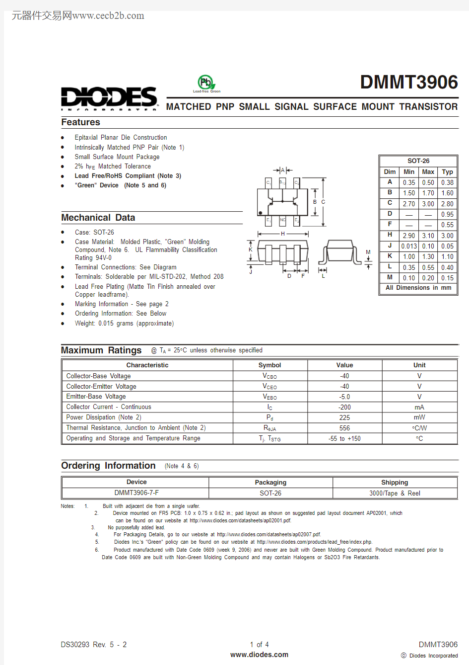
Mechanical Data
·Case: SOT-26
·Case Material: Molded Plastic, "Green" Molding Compound, Note 6. UL Flammability Classification Rating 94V-0
·Terminal Connections: See Diagram
·Terminals: Solderable per MIL-STD-202, Method 208·Lead Free Plating (Matte Tin Finish annealed over Copper leadframe).
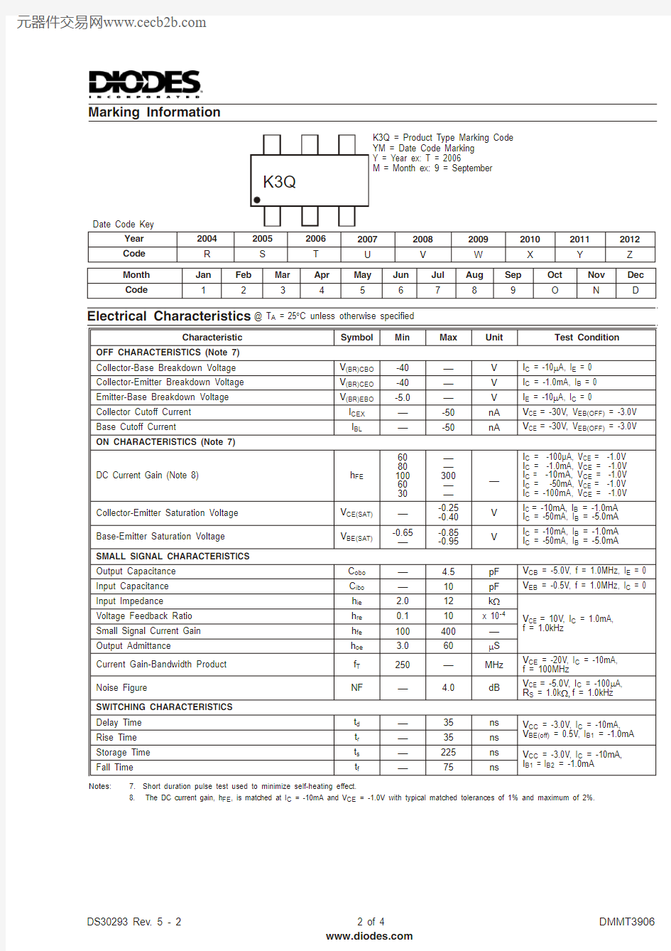
·Marking Information - See page 2·Ordering Information: See Below ·
Weight: 0.015 grams (approximate)
DMMT3906
MATCHED PNP SMALL SIGNAL SURFACE MOUNT TRANSISTOR
(Note 4 & 6)
Ordering Information
Features
·Epitaxial Planar Die Construction ·Intrinsically Matched PNP Pair (Note 1)·Small Surface Mount Package ·2% h FE Matched Tolerance
·Lead Free/RoHS Compliant (Note 3)·
"Green" Device (Note 5 and 6)
Notes:
7.Short duration pulse test used to minimize self-heating effect.
8. The DC current gain, h FE , is matched at I C = -10mA and V CE = -1.0V with typical matched tolerances of 1% and maximum of 2%.
K3Q = Product Type Marking Code YM = Date Code Marking Y = Year ex: T = 2006
M = Month ex: 9 = September
Marking Information
0.5
0.6
0.7
0.8
0.9
1.0
1
10
100
V , B A S E -E M I T T E R (V )B E (S A T ) S A T U R A T I O N V O L T A G E
I , COLLECTOR CURRENT (mA)C Fig. 5, Typical Base-Emitter
Saturation Voltage vs. Collector Current
10
1
1
10
100
1000
V , C O L L E C T O R -E M I T T E R (V )C E (S A T ) S A T U R A T I O N V O L T A G E
I , COLLECTOR CURRENT (mA)
C Fig. 4, Typical Collector-Emitter Saturation Voltage
vs. Collector Current
110
1000
100
0.1
1
10
1000
100
h , D C C U R R E N T G A I N
F E I , COLLECTOR CURRENT (mA)C Fig. 3, Typical DC Current Gain vs
Collector Current
100
10
0.1
110100
C , I N P U T C A P A C I T A N C E (p F )I B O C , O U T P U T C A P A C I T A N C E (p F )
O B O V , COLLECTOR-BASE VOLTAGE (V)CB
Fig. 2, Input and Output Capacitance vs.
Collector-Base Voltage
05010025
50
75
100
125
150
175
200
P , P O W E R D I S S I P A T I O N (m W )
D T , AMBIENT TEMPERATUR
E (°C)A Fig. 1, Max Power Dissipation vs Ambient Temperature, Total Device
1502002503003500
IMPORTANT NOTICE
Diodes Incorporated and its subsidiaries reserve the right to make modifications, enhancements, improvements, corrections or other changes without further notice to any product herein. Diodes Incorporated does not assume any liability arising out of the application or use of any product described herein; neither does it convey any license under its patent rights, nor the rights of others. The user of products in such applications shall assume all risks of such use and will agree to hold Diodes Incorporated and all the companies whose products are represented on our website, harmless against all damages.
LIFE SUPPORT
Diodes Incorporated products are not authorized for use as critical components in life support devices or systems without the expressed written approval of the President of Diodes Incorporated.