MAX3202EETT+中文资料
For pricing, delivery, and ordering information, please contact Maxim Direct at 1-888-629-4642,or visit Maxim's website at https://www.360docs.net/doc/4e16225631.html,.
General Description
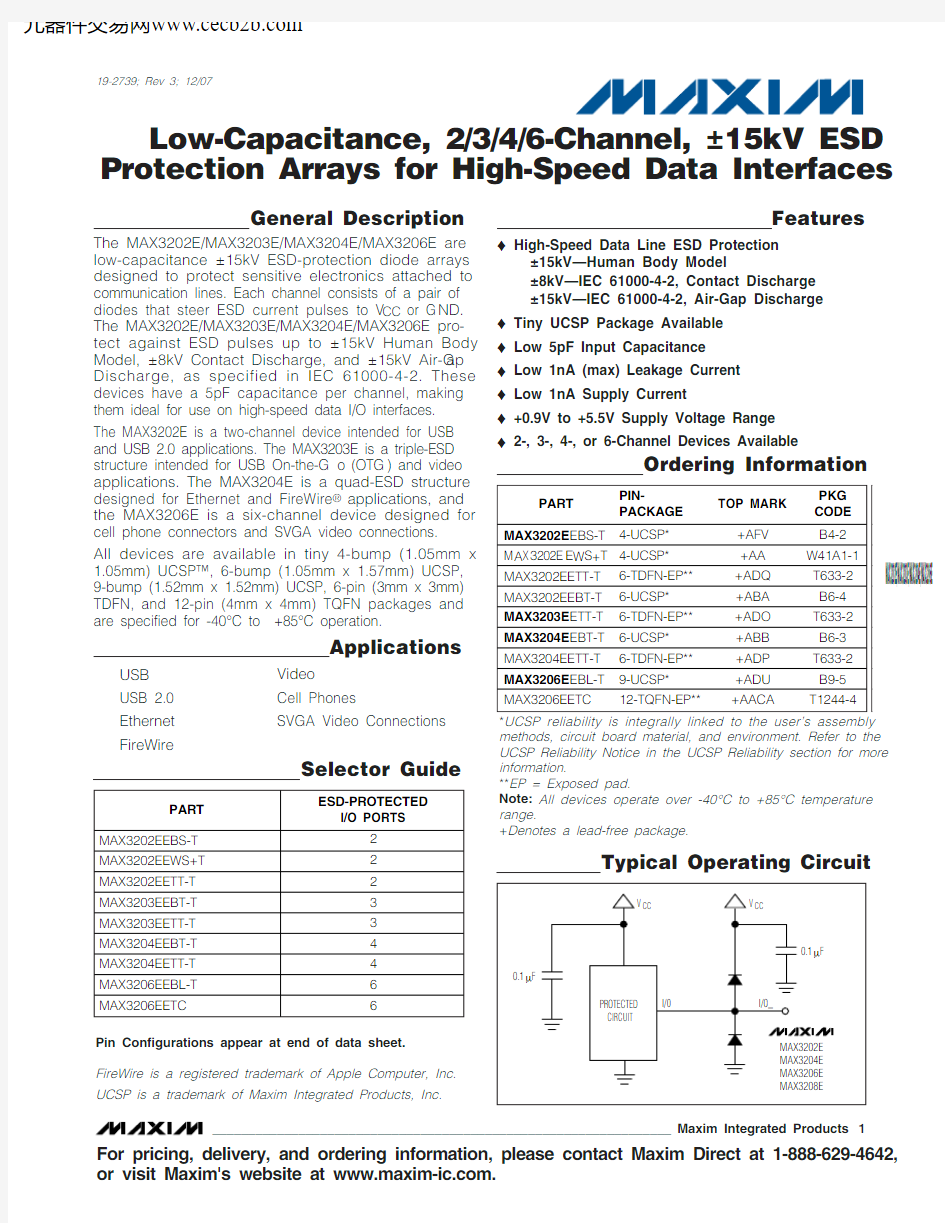
The MAX3202E/MAX3203E/MAX3204E/MAX3206E are low-capacitance ±15kV ESD-protection diode arrays designed to protect sensitive electronics attached to communication lines. Each channel consists of a pair of diodes that steer ESD current pulses to V CC or G ND.The MAX3202E/MAX3203E/MAX3204E/MAX3206E pro-tect against ESD pulses up to ±15kV Human Body Model, ±8kV Contact Discharge, and ±15kV Air-G ap Discharge, as specified in IEC 61000-4-2. These devices have a 5pF capacitance per channel, making them ideal for use on high-speed data I/O interfaces.The MAX3202E is a two-channel device intended for USB and USB 2.0 applications. The MAX3203E is a triple-ESD structure intended for USB On-the-G o (OTG ) and video applications. The MAX3204E is a quad-ESD structure designed for Ethernet and FireWire ?applications, and the MAX3206E is a six-channel device designed for cell phone connectors and SVGA video connections.All devices are available in tiny 4-bump (1.05mm x 1.05mm) UCSP?, 6-bump (1.05mm x 1.57mm) UCSP,9-bump (1.52mm x 1.52mm) UCSP, 6-pin (3mm x 3mm)TDFN, and 12-pin (4mm x 4mm) TQFN packages and are specified for -40°C to +85°C operation.
Applications
USB Video USB 2.0Cell Phones
Ethernet SVGA Video Connections
FireWire
Features
?High-Speed Data Line ESD Protection
±15kV—Human Body Model
±8kV—IEC 61000-4-2, Contact Discharge ±15kV—IEC 61000-4-2, Air-Gap Discharge ?Tiny UCSP Package Available ?Low 5pF Input Capacitance ?Low 1nA (max) Leakage Current ?Low 1nA Supply Current
?+0.9V to +5.5V Supply Voltage Range ?2-, 3-, 4-, or 6-Channel Devices Available
MAX3202E/MAX3203E/MAX3204E/MAX3206E
Low-Capacitance, 2/3/4/6-Channel, ±15kV ESD Protection Arrays for High-Speed Data Interfaces
________________________________________________________________Maxim Integrated Products 1
Ordering Information
19-2739; Rev 3; 12/07
methods, circuit board material, and environment. Refer to the UCSP Reliability Notice in the UCSP Reliability section for more information.
**EP = Exposed pad.
Note:All devices operate over -40°C to +85°C temperature range.
+Denotes a lead-free package.
Selector Guide
FireWire is a registered trademark of Apple Computer, Inc.UCSP is a trademark of Maxim Integrated Products, Inc.
Typical Operating Circuit
M A X 3202E /M A X 3203E /M A X 3204E /M A X 3206E
Low-Capacitance, 2/3/4/6-Channel, ±15kV ESD Protection Arrays for High-Speed Data Interfaces 2_______________________________________________________________________________________
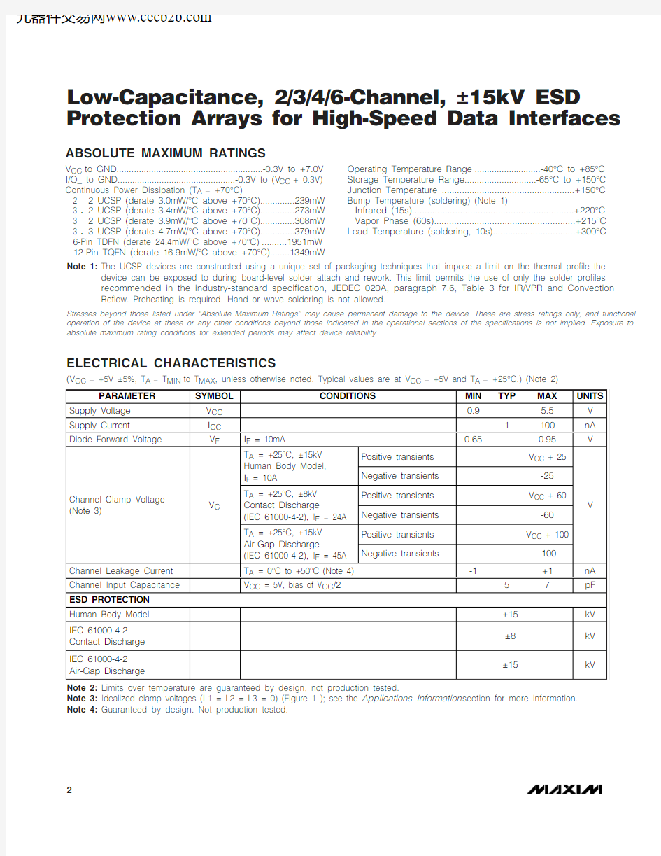
ABSOLUTE MAXIMUM RATINGS
ELECTRICAL CHARACTERISTICS
(V CC = +5V ±5%, T A = T MIN to T MAX , unless otherwise noted. Typical values are at V CC = +5V and T A = +25°C.) (Note 2)
Stresses beyond those listed under “Absolute Maximum Ratings” may cause permanent damage to the device. These are stress ratings only, and functional operation of the device at these or any other conditions beyond those indicated in the operational sections of the specifications is not implied. Exposure to absolute maximum rating conditions for extended periods may affect device reliability.
Note 2:Limits over temperature are guaranteed by design, not production tested.
Note 3:Idealized clamp voltages (L1 = L2 = L3 = 0) (Figure 1 ); see the Applications Information section for more information.Note 4:Guaranteed by design. Not production tested.
V CC to GND...........................................................-0.3V to +7.0V I/O_ to GND................................................-0.3V to (V CC + 0.3V)Continuous Power Dissipation (T A = +70°C)
2 ×2 UCSP (derate 3.0mW/°C above +70°C)..............239mW
3 ×2 UCSP (derate 3.4mW/°C above +70°C)..............273mW 3 ×2 UCSP (derate 3.9mW/°C above +70°C)..............308mW 3 ×3 UCSP (derate 4.7mW/°C above +70°C)..............379mW 6-Pin TDFN (derate 24.4mW/°C above +70°C)..........1951mW 12-Pin TQFN (derate 16.9mW/°C above +70°C)........1349mW
Operating Temperature Range ...........................-40°C to +85°C Storage Temperature Range.............................-65°C to +150°C Junction Temperature .....................................................+150°C Bump Temperature (soldering) (Note 1)
Infrared (15s)................................................................+220°C Vapor Phase (60s)........................................................+215°C Lead Temperature (soldering, 10s).................................+300°C
Note 1:The UCSP devices are constructed using a unique set of packaging techniques that impose a limit on the thermal profile the
device can be exposed to during board-level solder attach and rework. This limit permits the use of only the solder profiles recommended in the industry-standard specification, JEDEC 020A, paragraph 7.6, Table 3 for IR/VPR and Convection Reflow. Preheating is required. Hand or wave soldering is not allowed.
MAX3202E/MAX3203E/MAX3204E/MAX3206E
Low-Capacitance, 2/3/4/6-Channel, ±15kV ESD Protection Arrays for High-Speed Data Interfaces
_______________________________________________________________________________________3
Typical Operating Characteristics
(V CC = +5V, T A = +25°C, unless otherwise noted.)
0.30
0.700.501.100.901.301.50CLAMP VOLTAGE vs. DC CURRENT
M A X 3202E t o c 01
DC CURRENT (mA)
C L A M P V O L T A G E (V )30
70
90
50
110
130
150
1
10
100
1000
25
35
45
55
65
75
85
LEAKAGE CURRENT vs. TEMPERATURE
TEMPERATURE (°C)
L E
A K A G E C U R R E N T (p A )
24
8
6
10
12
2
1
3
4
5
INPUT CAPACITANCE vs. INPUT VOLTAGE
INPUT VOLTAGE (V)
I N P U T C A P A C I T A N C E (p F )
Detailed Description
The MAX3202E/MAX3203E/MAX3204E/MAX3206E are diode arrays designed to protect sensitive electronics against damage resulting from ESD conditions or tran-sient voltages. The low input capacitance makes these devices ideal for high-speed data lines. The MAX3202E, MAX3203E, MAX3204E, and MAX3206E protect two, three, four, and six channels, respectively.The MAX3202E/MAX3203E/MAX3204E/MAX3206E are designed to work in conjunction with a device’s intrinsic ESD protection. The MAX3202E/MAX3203E/MAX3204E/MAX3206E limit the excursion of the ESD event to below ±25V peak voltage when subjected to the Human Body Model waveform. When subjected to the IEC 61000-4-2 waveform, the peak voltage is limited to ±60V when subjected to Contact Discharge and ±100V when subjected to Air-Gap Discharge. The device that is being protected by the MAX3202E/MAX3203E/MAX3204E/MAX3206E must be able to withstand these peak voltages plus any additional voltage generated by the parasitic board.
Applications Information
Design Considerations
Maximum protection against ESD damage results from proper board layout (see the Layout Recommendations section and Figure 2). A good layout reduces the para-sitic series inductance on the ground line, supply line,and protected signal lines.
The MAX3202E/MAX3203E/MAX3204E/MAX3206E ESD diodes clamp the voltage on the protected lines during an ESD event and shunt the current to GND or V CC . In an ideal circuit, the clamping voltage, V C , is defined as the forward voltage drop, V F , of the protection diode plus any supply voltage present on the cathode.For positive ESD pulses:
V C = V CC + V F
For negative ESD pulses:
V C = -V F
In reality, the effect of the parasitic series inductance on the lines must also be considered (Figure 1).For positive ESD pulses:
For negative ESD pulses:
where I ESD
is the ESD current pulse.
M A X 3202E /M A X 3203E /M A X 3204E /M A X 3206E
Low-Capacitance, 2/3/4/6-Channel, ±15kV ESD Protection Arrays for High-Speed Data Interfaces 4
_______________________________________________________________________________________
Figure 1. Parasitic Series Inductance
Figure 2. Layout Considerations
MAX3202E/MAX3203E/MAX3204E/MAX3206E
Low-Capacitance, 2/3/4/6-Channel, ±15kV ESD Protection Arrays for High-Speed Data Interfaces
_______________________________________________________________________________________
5
During an ESD event, the current pulse rises from zero to peak value in nanoseconds (Figure 3). For example,in a 15kV IEC-61000 Air-G ap Discharge ESD event,the pulse current rises to approximately 45A in 1ns (di/dt = 45 x 109). An inductance of only 10nH adds an additional 450V to the clamp voltage. An inductance of 10nH represents approximately 0.5in of board trace.Regardless of the device’s specified diode clamp volt-age, a poor layout with parasitic inductance significantly increases the effective clamp voltage at the protected signal line.
A low-ESR 0.1μF capacitor must be used between V CC and G ND. This bypass capacitor absorbs the charge transferred by an +8kV IEC-61000 Contact Discharge ESD event.
Ideally, the supply rail (V CC ) would absorb the charge caused by a positive ESD strike without changing its regulated value. In reality, all power supplies have an effective output impedance on their positive rails. If a power supply’s effective output impedance is 1Ω, then by using V = I ×R, the clamping voltage of V C increas-es by the equation V C = I ESD x R OUT . An +8kV IEC 61000-4-2 ESD event generates a current spike of 24A,so the clamping voltage increases by V C = 24A ×1Ω,or V C = 24V. Again, a poor layout without proper bypassing increases the clamping voltage. A ceramic chip capacitor mounted as close to the MAX3202E/MAX3203E/MAX3204E/MAX3206E V CC pin is the best choice for this application. A bypass capacitor should also be placed as close to the protected device as possible.
±15kV ESD Protection
ESD protection can be tested in various ways; the MAX3202E/MAX3203E/MAX3204E/MAX3206E are characterized for protection to the following limits:
?±15kV using the Human Body Model
?±8kV using the Contact Discharge method speci-fied in IEC 61000-4-2?±15kV using the IEC 61000-4-2 Air-Gap Discharge method
ESD Test Conditions
ESD performance depends on a number of conditions.Contact Maxim for a reliability report that documents test setup, methodology, and results.
Human Body Model
Figure 4 shows the Human Body Model, and Figure 5shows the current waveform it generates when dis-charged into a low impedance. This model consists of a 100pF capacitor charged to the ESD voltage of inter-est, which is then discharged into the device through a 1.5k Ωresistor.
Figure 4. Human Body ESD Test Model
Figure 3. IEC 61000-4-2 ESD Generator Current Waveform
M A X 3202E /M A X 3203E /M A X 3204E /M A X 3206E
IEC 61000-4-2
The IEC 61000-4-2 standard covers ESD testing and performance of finished equipment. The MAX3202E/MAX3203E/MAX3204E/MAX3206E help users design equipment that meets Level 4 of IEC 61000-4-2.
The main difference between tests done using the Human Body Model and IEC 61000-4-2 is higher peak current in IEC 61000-4-2. Because series resistance is lower in the IEC 61000-4-2 ESD test model (Figure 6)the ESD-withstand voltage measured to this standard is generally lower than that measured using the Human Body Model. Figure 3 shows the current waveform for the ±8kV IEC 61000-4-2 Level 4 ESD Contact Discharge test.
The Air-G ap Discharge test involves approaching the device with a charged probe. The Contact Discharge method connects the probe to the device before the probe is energized.
Layout Recommendations
Proper circuit-board layout is critical to suppress ESD-induced line transients. The MAX3202E/MAX3203E/MAX3204E/MAX3206E clamp to 100V; however, with improper layout, the voltage spike at the device is much higher. A lead inductance of 10nH with a 45A current spike at a dv/dt of 1ns results in an ADDITION-AL 450V spike on the protected line. It is essential that the layout of the PC board follows these guidelines:
1)Minimize trace length between the connector or input terminal, I/O_, and the protected signal line.2)Use separate planes for power and ground to reduce parasitic inductance and to reduce the impedance to the power rails for shunted ESD current.
3)Ensure short ESD transient return paths to G ND and V CC .4)Minimize conductive power and ground loops.
5)Do not place critical signals near the edge of the PC board.
6)Bypass V CC to GND with a low-ESR ceramic capac-itor as close to V CC as possible.
7)Bypass the supply of the protected device to G ND with a low-ESR ceramic capacitor as close to the supply pin as possible.
UCSP Considerations
For general UCSP package information and PC layout considerations, refer to Maxim Application Note 263,Wafer-Level Chip-Scale Package .
___________________UCSP Reliability
The UCSP represents a unique packaging form factor that may not perform equally to a packaged product through traditional mechanical reliability tests. UCSP reliability is integrally linked to the user’s assembly meth-ods, circuit-board material, and usage environment.
The user should closely review these areas when con-sidering use of a UCSP. Performance through operat-ing life test and moisture resistance remains uncompromised as it is primarily determined by the wafer-fabrication process. Mechanical stress perfor-mance is a greater consideration for a UCSP. UCSPs are attached through direct solder contact to the user’s PC board, foregoing the inherent stress relief of a pack-aged product lead frame. Solder-joint contact integrity must be considered. Table 1 shows the testing done to characterize the UCSP reliability performance. In con-clusion, the UCSP is capable of performing reliably through environmental stresses as indicated by the results in the table. Additional usage data and recom-mendations are detailed in the UCSP application note,which can be found on Maxim’s website at https://www.360docs.net/doc/4e16225631.html,.
Chip Information
PROCESS: BiCMOS
Low-Capacitance, 2/3/4/6-Channel, ±15kV ESD Protection Arrays for High-Speed Data Interfaces 6_______________________________________________________________________________________
Figure 6. IEC 61000-4-2 ESD Test Model
MAX3202E/MAX3203E/MAX3204E/MAX3206E
Low-Capacitance, 2/3/4/6-Channel, ±15kV ESD Protection Arrays for High-Speed Data Interfaces
_______________________________________________________________________________________7
Functional Diagrams
M A X 3202E /M A X 3203E /M A X 3204E /M A X 3206E
Low-Capacitance, 2/3/4/6-Channel, ±15kV ESD Protection Arrays for High-Speed Data Interfaces 8_______________________________________________________________________________________
Pin Configurations
MAX3202E/MAX3203E/MAX3204E/MAX3206E
Low-Capacitance, 2/3/4/6-Channel, ±15kV ESD Protection Arrays for High-Speed Data Interfaces
_______________________________________________________________________________________9
Package Information
(The package drawing(s) in this data sheet may not reflect the most current specifications. For the latest package outline information go to https://www.360docs.net/doc/4e16225631.html,/packages .)
M A X 3202E /M A X 3203E /M A X 3204E /M A X 3206E
Low-Capacitance, 2/3/4/6-Channel, ±15kV ESD Protection Arrays for High-Speed Data Interfaces 10______________________________________________________________________________________
Package Information (continued)
(The package drawing(s) in this data sheet may not reflect the most current specifications. For the latest package outline information go to https://www.360docs.net/doc/4e16225631.html,/packages .)
MAX3202E/MAX3203E/MAX3204E/MAX3206E
Low-Capacitance, 2/3/4/6-Channel, ±15kV ESD Protection Arrays for High-Speed Data Interfaces
______________________________________________________________________________________11
Package Information (continued)
(The package drawing(s) in this data sheet may not reflect the most current specifications. For the latest package outline information go to https://www.360docs.net/doc/4e16225631.html,/packages .)
M A X 3202E /M A X 3203E /M A X 3204E /M A X 3206E
Low-Capacitance, 2/3/4/6-Channel, ±15kV ESD Protection Arrays for High-Speed Data Interfaces 12
______________________________________________________________________________________
Package Information (continued)
(The package drawing(s) in this data sheet may not reflect the most current specifications. For the latest package outline information go to https://www.360docs.net/doc/4e16225631.html,/packages .)
MAX3202E/MAX3203E/MAX3204E/MAX3206E
Low-Capacitance, 2/3/4/6-Channel, ±15kV ESD Protection Arrays for High-Speed Data Interfaces
Package Information (continued)
(The package drawing(s) in this data sheet may not reflect the most current specifications. For the latest package outline information go to https://www.360docs.net/doc/4e16225631.html,/packages .)
M A X 3202E /M A X 3203E /M A X 3204E /M A X 3206E
Low-Capacitance, 2/3/4/6-Channel, ±15kV ESD Protection Arrays for High-Speed Data Interfaces 14
______________________________________________________________________________________
Package Information (continued)
(The package drawing(s) in this data sheet may not reflect the most current specifications. For the latest package outline information go to https://www.360docs.net/doc/4e16225631.html,/packages .)
MAX3202E/MAX3203E/MAX3204E/MAX3206E
Low-Capacitance, 2/3/4/6-Channel, ±15kV ESD Protection Arrays for High-Speed Data Interfaces
______________________________________________________________________________________15
Package Information (continued)
(The package drawing(s) in this data sheet may not reflect the most current specifications. For the latest package outline information go to https://www.360docs.net/doc/4e16225631.html,/packages
.)
M A X 3202E /M A X 3203E /M A X 3204E /M A X 3206E
Low-Capacitance, 2/3/4/6-Channel, ±15kV ESD Protection Arrays for High-Speed Data Interfaces Maxim cannot assume responsibility for use of any circuitry other than circuitry entirely embodied in a Maxim product. No circuit patent licenses are implied. Maxim reserves the right to change the circuitry and specifications without notice at any time.
16_____________________________Maxim Integrated Products, 120 San Gabriel Drive, Sunnyvale, CA 94086 408-737-7600?2007 Maxim Integrated Products
is a registered trademark of Maxim Integrated Products, Inc.