uPSD3233BV-24U6T中文资料
1/6
DATA BRIEFING
September 2003
UPSD3234A, UPSD3234BV UPSD3233B, UPSD3233BV
Flash Programmable System Devices
with 8032 Microcontroller Core
FEATURES SUMMARY
s The uPSD323X Devices combine a Flash PSD architecture with an 8032 microcontroller core.The uPSD323X Devices of Flash PSDs feature dual banks of Flash memory, SRAM, general purpose I/O and programmable logic, supervi-sory functions and access via USB, I 2C, ADC,DDC and PWM channels, and an on-board 8032 microcontroller core, with two UARTs,three 16-bit Timer/Counters and two External Interrupts. As with other Flash PSD families, the uPSD323X Devices are also in-system pro-grammable (ISP) via a JTAG ISP interface.s Large 8KByte SRAM with battery back-up option
s
Dual bank Flash memories
–128KByte or 256KByte main Flash memory –32KByte secondary Flash memory
s
Content Security
–Block access to Flash memory
s
Programmable Decode PLD for flexible address mapping of all memories within 8032 space.s High-speed clock standard 8032 core (12-cycle)s USB Interface (some devices only)s I 2C interface for peripheral connections s 5 Pulse Width Modulator (PWM) channels s Analog-to-Digital Converter (ADC)s Standalone Display Data Channel (DDC)s Six I/O ports with up to 46 I/O pins s 3000 gate PLD with 16 macrocells s Supervisor functions with Watchdog Timer s In-System Programming (ISP) via JTAG s Zero-Power Technology s
Single Supply Voltage –4.5 to 5.5V –3.0 to 3.6V
UPSD3234A, UPSD3234BV, UPSD3233B, UPSD3233BV
2/6
SUMMARY DESCRIPTION s Dual bank Flash memories
–Concurrent operation, read from memory while erasing and writing the other. In-Appli-cation Programming (IAP) for remote updates –Large 128KByte or 256KByte main Flash memory for application code, operating sys-tems, or bit maps for graphic user interfaces –Large 32KByte secondary Flash memory di-vided in small sectors. Eliminate external EE-PROM with software EEPROM emulation –Secondary Flash memory is large enough for sophisticated communication protocol (USB)during IAP while continuing critical system tasks
s
Large SRAM with battery back-up option –8KByte SRAM for RTOS, high-level languag-es, communication buffers, and stacks
s
Programmable Decode PLD for flexible address mapping of all memories
–Place individual Flash and SRAM sectors on any address boundary –Built-in page register breaks restrictive 8032limit of 64KByte address space –Special register swaps Flash memory seg-ments between 8032 “program” space and “data” space for efficient In-Application Pro-gramming
s
High-speed clock standard 8032 core (12-cycle)–40MHz operation at 5V, 24MHz at 3.3V –2 UARTs with independent baud rate, three 16-bit Timer/Counters and two External Inter-rupts
s
USB Interface (uPSD3234A-40 only)–Supports USB 1.1 Slow Mode (1.5Mbit/s)–Control endpoint 0 and interrupt endpoints 1and 2
s
I 2C interface for peripheral connections –Capable of master or slave operation s
5 Pulse Width Modulator (PWM) channels –Four 8-bit PWM units
–One 8-bit PWM unit with programmable peri-od
s
4-channel, 8-bit Analog-to-Digital Converter (ADC) with analog supply voltage (V REF )s
Standalone Display Data Channel (DDC)–For use in monitor, projector, and TV applica-tions –Compliant with VESA standards DDC1 and DDC2B –Eliminate external DDC PROM
s
Six I/O ports with up to 46 I/O pins
–Multifunction I/O: GPIO, DDC, I 2C, PWM,PLD I/O, supervisor, and JTAG –Eliminates need for external latches and logic
s
3000 gate PLD with 16 macrocells
–Create glue logic, state machines, delays,etc.–Eliminate external PALs, PLDs, and 74HCxx –Simple PSDsoft Express software ...Free
s
Supervisor functions
–Generates reset upon low voltage or watch-dog time-out. Eliminate external supervisor device –s
In-System Programming (ISP) via JTAG –Program entire chip in 10 - 25 seconds with no involvement of 8032–Allows efficient manufacturing, easy product testing, and Just-In-Time inventory –Eliminate sockets and pre-programmed parts –Program with FlashLINK TM cable and any PC
s
Content Security
–Programmable Security Bit blocks access of device programmers and readers
s
Zero-Power Technology
–Memories and PLD automatically reach standby current between input changes
s
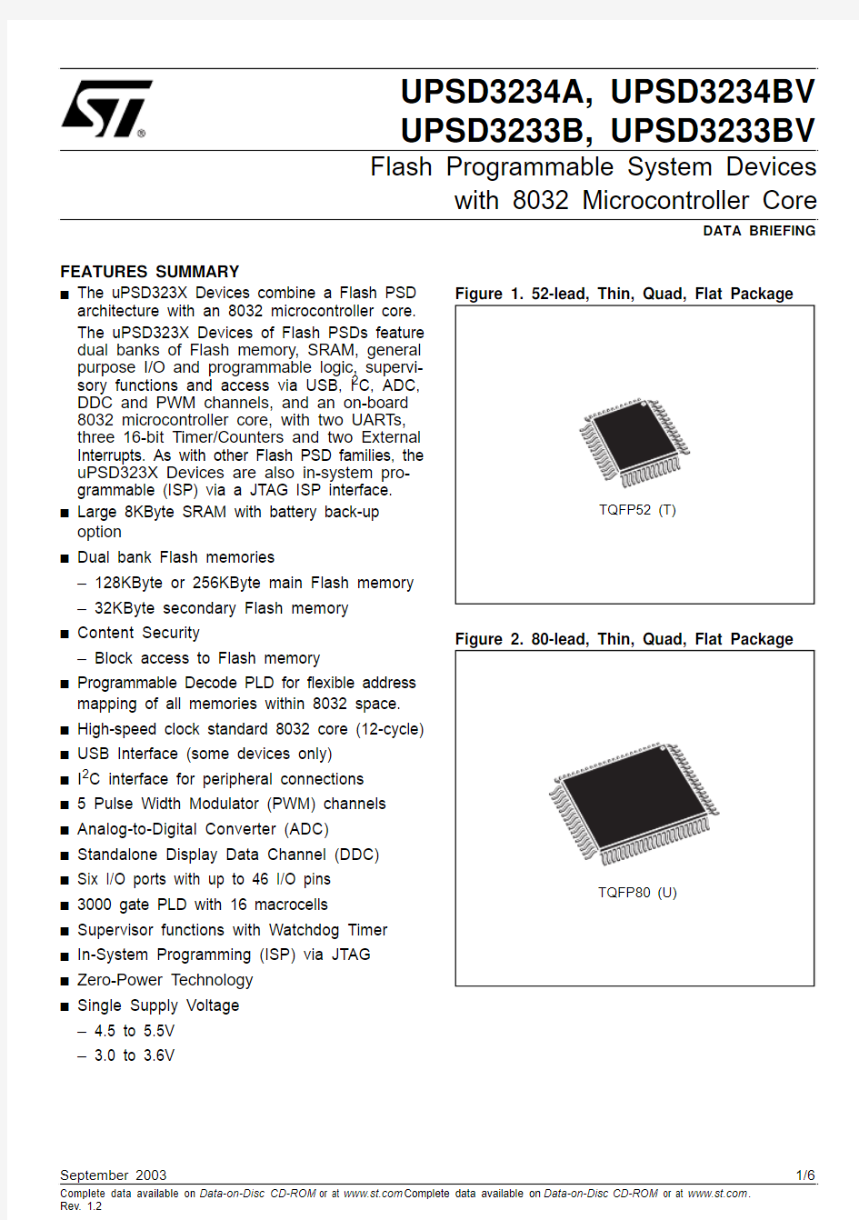
Packages –52-pin TQFP
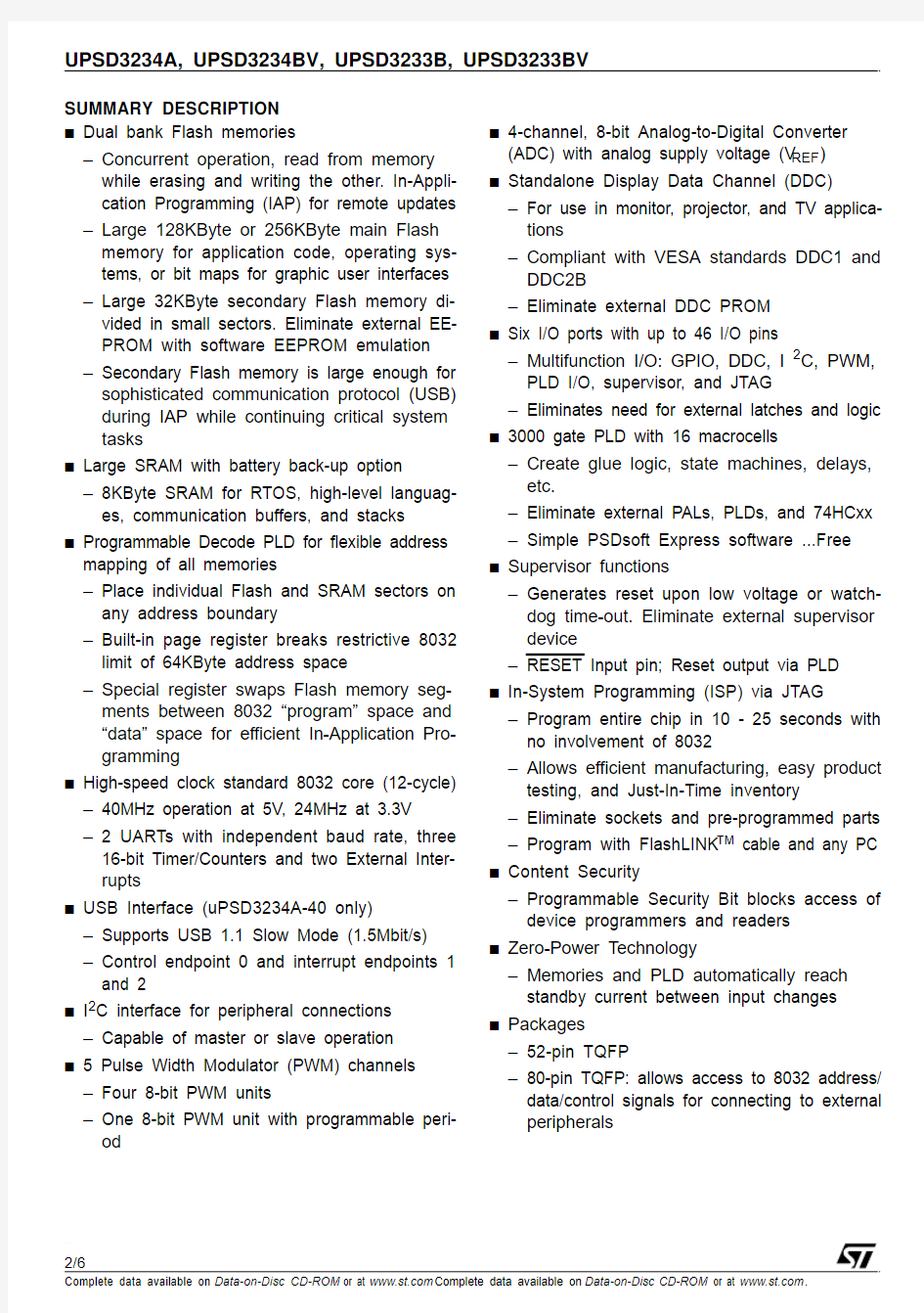
–80-pin TQFP: allows access to 8032 address/data/control signals for connecting to external peripherals
3/6
UPSD3234A, UPSD3234BV, UPSD3233B, UPSD3233BV
Table 1. uPSD323X Devices Product Matrix
Note: 1.Pull-up resistor required on pin 5 (2k ? for 3V devices, 7.5k ? for 5V devices) for all 52-pin devices, with or without USB function.
2.Pin 7 is Not Connected (NC) for device with no USB function.
Part No.Main Flash (bit)Sec.
Flash (bit)SRAM (bit)Macro -Cells I/O Pins PWM Ch.Timer / Ctr UART Ch.I 2
C ADC Ch.DDC USB
V CC
MHz Pins
uPSD
3234A-402M
256K
64K
16
37 or 46
5
3
2
1
4
yes
yes 5V 40
52 or 80
uPSD 3234BV-242M 256K 64K 164653214yes 3V 2480
uPSD 3233B-401M 256K 64K 16
37 or 4653214yes 5V 40
52 or 80uPSD 3233BV-24
1M 256K 64K 1637 or 46
53214yes 3V 24
52 or 80
UPSD3234A, UPSD3234BV, UPSD3233B, UPSD3233BV
1.Pull-up resistor required on pin 8 (2k? for 3V devices, 7.5k? for 5V devices) for all 82-pin devices, with or without USB function.
2.Pin 10 is Not Connected (NC) for device with no USB function.
4/6
UPSD3234A, UPSD3234BV, UPSD3233B, UPSD3233BV
For ceramic resonators, contact resonator manufacturer
Oscillation circuit is designed to be used either with a ceramic resonator or crystal oscillator. Since each crystal and ceramic resonator have their own characteristics, the user should consult the crystal manufacturer for appropriate values of external components.
5/6
UPSD3234A, UPSD3234BV, UPSD3233B, UPSD3233BV
PART NUMBERING
Table 2. Ordering Information Scheme
Example:uPSD3234B V–24U6T
Device Type
uPSD = Microcontroller PSD
Family
3 = 8032 core
PLD Size
2 = 16 Macrocells
SRAM Size
3 = 64Kbit
Main Flash Memory Size
3 = 1Mbit
4 = 2Mbit
IP Mix
A = USB, I2C, PWM, DDC, ADC, (2) UARTs
Supervisor (Reset Out, Reset In, LVD, WD)
B = I2C, PWM, DDC, ADC, (2) UARTs
Supervisor (Reset Out, Reset In, LVD, WD)
Operating Voltage
blank = V CC = 4.5 to 5.5V
V = V CC = 3.0 to 3.6V
Speed
–24 = 24MHz
–40 = 40MHz
Package
T = 52-pin TQFP
U = 80-pin TQFP
Temperature Range
1 = 0 to 70°C
6 = –40 to 85°C
Shipping Optio n
Tape & Reel Packing = T
For a list of available options (e.g., Speed, Package) or for further information on any aspect of this device, please contact the ST Sales Office nearest to you.
6/6