Room-Temperature Ultraviolet Nanowire Nanolasers
DOI: 10.1126/science.1060367
, 1897 (2001);
292Science et al.Michael H. Huang,Room-Temperature Ultraviolet Nanowire Nanolasers
https://www.360docs.net/doc/591877894.html, (this information is current as of June 3, 2008 ):The following resources related to this article are available online at
https://www.360docs.net/doc/591877894.html,/cgi/content/full/292/5523/1897version of this article at:
including high-resolution figures, can be found in the online Updated information and services,found at:
can be related to this article A list of selected additional articles on the Science Web sites https://www.360docs.net/doc/591877894.html,/cgi/content/full/292/5523/1897#related-content https://www.360docs.net/doc/591877894.html,/cgi/content/full/292/5523/1897#otherarticles , 1 of which can be accessed for free:
cites 14 articles This article 2334 article(s) on the ISI Web of Science. cited by This article has been https://www.360docs.net/doc/591877894.html,/cgi/content/full/292/5523/1897#otherarticles 5 articles hosted by HighWire Press; see: cited by This article has been
https://www.360docs.net/doc/591877894.html,/cgi/collection/app_physics Physics, Applied
: subject collections This article appears in the following
https://www.360docs.net/doc/591877894.html,/about/permissions.dtl in whole or in part can be found at: this article permission to reproduce of this article or about obtaining reprints Information about obtaining registered trademark of AAAS.
is a Science 2001 by the American Association for the Advancement of Science; all rights reserved. The title Copyright American Association for the Advancement of Science, 1200 New York Avenue NW, Washington, DC 20005. (print ISSN 0036-8075; online ISSN 1095-9203) is published weekly, except the last week in December, by the Science o n J u n e 3, 2008
w w w .s c i e n c e m a g .o r g D o w n l o a d e d f r o m
Room-Temperature Ultraviolet
Nanowire Nanolasers
Michael H.Huang,1Samuel Mao,2Henning Feick,3Haoquan Yan,1
Yiying Wu,1Hannes Kind,1Eicke Weber,3Richard Russo,2
Peidong Yang 1,3*
Room-temperature ultraviolet lasing in semiconductor nanowire arrays has been demonstrated.The self-organized,?0001?oriented zinc oxide nanowires grown on sapphire substrates were synthesized with a simple vapor transport and condensation process.These wide band-gap semiconductor nanowires form natural laser cavities with diameters varying from 20to 150nanometers and lengths up to 10micrometers.Under optical excitation,surface-emitting lasing action was observed at 385nanometers,with an emission linewidth less than 0.3nanometer.The chemical ?exibility and the one-dimensionality of the nanowires make them ideal miniaturized laser light sources.These short-wave-length nanolasers could have myriad applications,including optical computing,information storage,and microanalysis.The interest in developing short-wavelength semiconductor lasers has culminated in the realization of room-temperature green-blue
diode laser structures with ZnSe and In x -Ga 1-x N as the active layers (1–3).ZnO is a wide band-gap (3.37eV)compound semi-conductor that is suitable for blue optoelec-tronic applications,with ultraviolet lasing ac-tion being reported (4–6)in disordered par-ticles and thin films.For wide band-gap semiconductor materials,a high carrier con-centration is usually required in order to reach an optical gain that is high enough for
lasing action in an electron-hole plasma (EHP)process (7).Such an EHP mechanism,which is common for conventional laser di-ode operation,typically requires high lasing thresholds.As an alternative to an EHP pro-cess,excitonic recombination in semiconduc-tors is a more efficient radiative process and can facilitate low-threshold stimulated emis-sion (8,9).To achieve efficient excitonic laser action at room temperature,the binding energy of the exciton must be much greater than the thermal energy at room temperature (26meV ).In this regard,ZnO is a good candidate because its exciton binding energy is ?60meV,substantially larger than that of ZnSe (22meV )and GaN (25meV ).
To further lower the threshold,low-di-mensional compound semiconductor nano-structures have been fabricated,in which quantum size effects yield a substantial den-sity of states at the band edges and enhance radiative recombination due to carrier con-finement.The use of semiconductor quantum well structures as low-threshold optical gain media represents a sizable advancement in semiconductor laser technology (10).Light emission from semiconductor nanowhiskers has been previously reported in GaAs and GaP systems (11,12).Stimulated emission and optical gain have also been demonstrated recently in Si and CdSe nanoclusters and their ensembles (13,14).Here,we demon-
1Department of Chemistry,University of California,2
Environmental Energy Technology Division,3Materi-als Science Division,Lawrence Berkeley National Lab-oratory,Berkeley,CA 94720,USA.
*To whom correspondence should be addressed.E-mail:
pyang@https://www.360docs.net/doc/591877894.html,
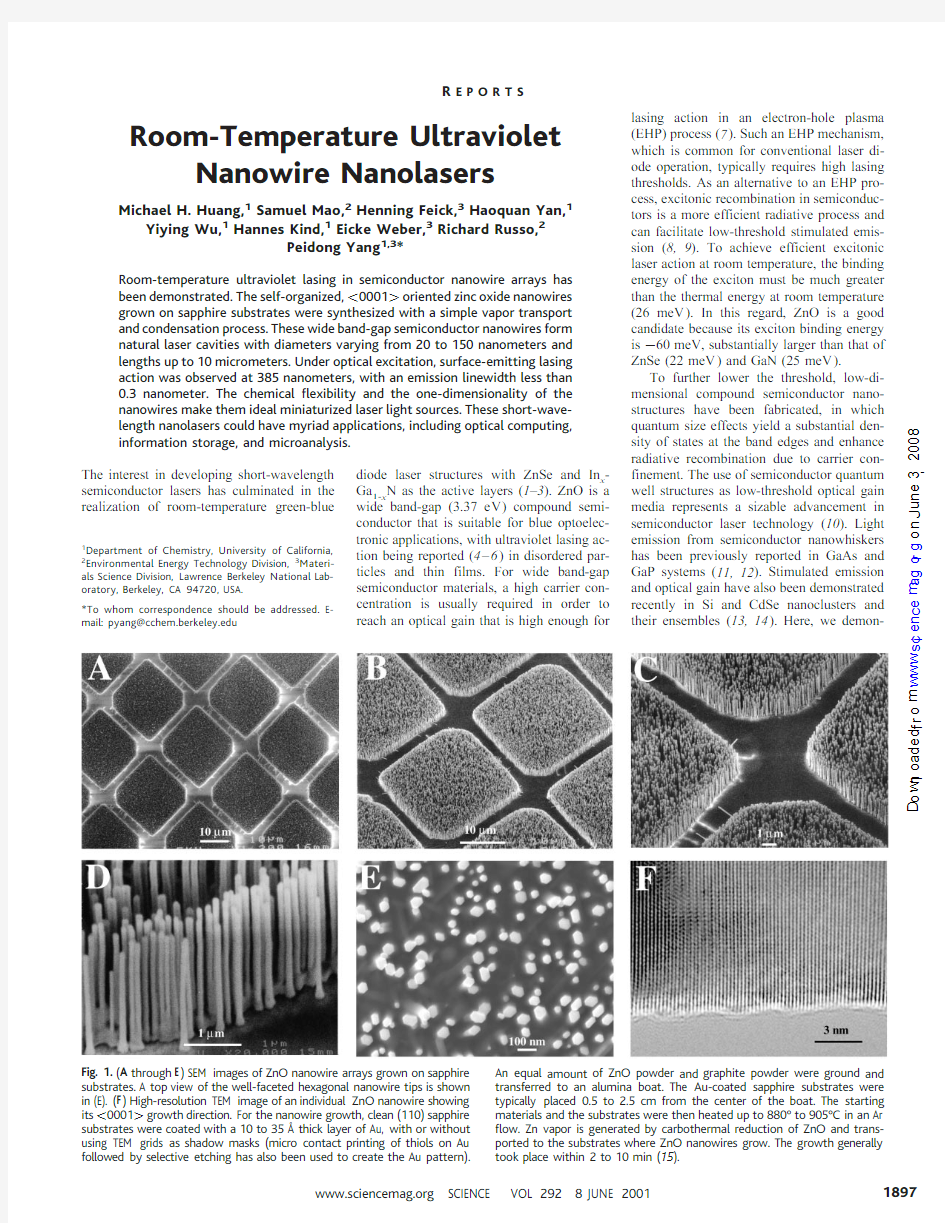
Fig.1.(A through E )SEM images of ZnO nanowire arrays grown on sapphire substrates.A top view of the well-faceted hexagonal nanowire tips is shown in (E).(F )High-resolution TEM image of an individual ZnO nanowire showing its ?0001?growth direction.For the nanowire growth,clean (110)sapphire substrates were coated with a 10to 35?thick layer of Au,with or without using TEM grids as shadow masks (micro contact printing of thiols on Au followed by selective etching has also been used to create the Au pattern).An equal amount of ZnO powder and graphite powder were ground and transferred to an alumina boat.The Au-coated sapphire substrates were typically placed 0.5to 2.5cm from the center of the boat.The starting materials and the substrates were then heated up to 880°to 905°C in an Ar ?ow.Zn vapor is generated by carbothermal reduction of ZnO and trans-ported to the substrates where ZnO nanowires grow.The growth generally took place within 2to 10min (15).
https://www.360docs.net/doc/591877894.html, SCIENCE VOL 2928JUNE 20011897
o n J u n e 3, 2008
w w w .s c i e n c e m a g .o r g D o w n l o a d e d f r o m
strate excitonic lasing action in ZnO nano-wires with a threshold of 40kW/cm 2under optical excitation.
ZnO nanowires were synthesized with a vapor phase transport process via catalyzed epitaxial crystal growth (15).Using Au thin film as the catalysts for nanowire growth,we epitaxially grew the nanowires,which are highly oriented,on the substrate.Selective nanowire growth can be readily achieved by patterning the Au thin film before growth.Typical scanning electron microscopy (SEM)images of nanowire arrays grown on sapphire (110)substrates with patterned Au thin film (Fig.1)confirm that the ZnO nanowires grow only in the Au-coated areas.The diameters of these wires range from 20to 150nm,whereas more than 95%of them have diameters of 70to 100nm.The diameter dispersity is due to the inhomogeneous sizes of the Au nanoclus-ter catalysts when the substrate is annealed during the growth process.The lengths of these nanowires can be varied between 2and 10?m by adjusting the growth time.The capability of patterned nanowire growth al-lows us to fabricate nanoscale light emitters on the substrate in a controllable fashion.Because of the good epitaxial interface between the (0001)plane of the ZnO nano-wire and the (110)plane of the substrate (16),nearly all of the nanowires grow vertically from the substrates (Fig.1,A through D).The a plane (110)of sapphire is twofold symmet-ric,whereas the ZnO c plane is sixfold sym-metric.They are essentially incommensurate,with the exception that the a axis of ZnO and the c axis of sapphire are related almost exactly by a factor of 4,with a mismatch of less than 0.08%at room temperature.Such a coincidental matchup along the sapphire [0001]direction,along with a strong tenden-cy of ZnO to grow in the c orientation and the incoherence of interfaces in directions other than sapphire [0001],leads to the unique vertical epitaxial growth configuration.The anisotropy of the sapphire’s a plane is critical
for growing high-quality c -oriented ZnO nanowire arrays.
Hexagon end planes of the nanowires can be clearly identified in the SEM image of the nanowire array (Fig.1E),providing strong evidence that these nanowires grow along the ?0001?direction and are indeed well-facet-ed at both the end and side surfaces.The well-faceted nature of these nanowires will have important implications when they are used as effective laser media.Additional structural characterization of the ZnO nano-wires was carried out with transmission elec-tron microscopy (TEM).The high-resolution TEM image of a single-crystalline ZnO nanowire (Fig.1F)shows that spacing of 2.56?0.05?between adjacent lattice planes corresponds to the distance between two (0002)crystal planes,further proving ?0001?to be the preferred growth direction for the ZnO nanowires.This ?0001?pref-erential nanowire growth on the sapphire sub-strate is also reflected in the x-ray diffraction pattern (Fig.2).Only (000l )peaks are ob-served,indicating excellent overall c -axis alignment of these nanowire arrays over a large substrate area.
Photoluminescence spectra of nanowires were measured with a He-Cd laser (325nm)as an excitation source.Strong near–band-gap edge emission at ?377nm has been observed (15).In order to explore the possi-ble stimulated emission from these oriented nanowires,the power-dependent emission has been examined.The samples were opti-cally pumped by the fourth harmonic of Nd:yttrium-aluminum-garnet laser (266nm,3-ns pulse width)at room temperature.The pump beam was focused on nanowires at an inci-dence angle 10°to the symmetric axis of the nanowire.Light emission was collected in the direction normal to the end surface plane (along the symmetric axis)of the nanowires.In the absence of any fabricated mirrors,we observed lasing action in these ZnO nano-wires during the evolution of the emission spectra with increasing pump power (Fig.3,A and B).At low excitation intensity,the spectrum consists of a single broad spontane-ous emission peak (Fig.3A)with a full width at half maximum of ?17nm.This spontane-ous emission is 140meV below the band gap (3.37eV )and is generally ascribed to the recombination of excitons through an exci-ton-exciton collision process,where one of the excitons radiatively recombines to gener-ate a photon (4–6).As the pump power in-creases,the emission peak narrows because of the preferential amplification of frequencies close to the maximum of the gain
spectrum.
Fig.2.X-ray diffraction pattern of ZnO nano-wires on a sapphire substrate.Only (000l )peaks are observed,owing to their well-orient-ed growth con?guration.The diffraction pat-tern is taken on a Siemens Z5000x-ray diffrac-tometer.a.u.,arbitrary
units.
Fig.3.(A )Emission spectra from nanowire arrays below (line a)and above (line b and inset)the lasing threshold.The pump power for these spectra are 20,100,and 150kW/cm 2,respectively.The spectra are offset for easy comparison.(B )Integrated emission intensity from nanowires as a function of optical pumping energy intensity.(C )Schematic illustration of a nanowire as a resonance cavity with two naturally faceted hexagonal end faces acting as re?ecting mirrors.Stimulated emission from the nanowires was collected in the direction along the nanowire’s end-plane normal (the symmetric axis)with a monochromator (ISA,Edison,New Jersey)combined with a Peltier-cooled charge-coupled device (EG&G,Gaithersburg,Maryland).The 266-nm pump beam was focused to the nanowire array at an angle 10°to the end-plane normal.All experiments were carried out at room temperature.
8JUNE 2001VOL 292SCIENCE https://www.360docs.net/doc/591877894.html,
1898 o n J u n e 3, 2008
w w w .s c i e n c e m a g .o r g D o w n l o a d e d f r o m
When the excitation intensity exceeds a thresh-old (?40kW/cm 2),sharp peaks emerge in the emission spectra.The linewidths of these peaks are ?0.3nm,which are ?50times smaller than the linewidth of the spontaneous emission peak below the threshold.Above the threshold,the integrated emission intensity increases rapidly with the pump power (Fig.3B).The narrow linewidth and the rapid increase of emission intensity indicate that stimulated emission takes place in these nanowires.The observed single or multiple sharp peaks represent different las-ing modes at wavelengths between 370and 400nm.The lasing threshold is quite low in com-parison with previously reported values for ran-dom lasing (?300kW/cm 2)in disordered par-ticles or thin films (4).These short-wavelength nanowire nanolasers operate at room tempera-ture,and the areal density of these nanolasers readily reaches 1.1?1010cm ?2.
The observation of lasing action in these nanowire arrays without any fabricated mir-ror prompts us to consider these single-crys-talline,well-faceted nanowires as natural res-onance cavities (Fig.3C).It is possible that the giant oscillator strength effect (8),which can occur in high-quality nanowire crystals with dimensions larger than the exciton Bohr radius but smaller than the optical wave-length,enables the excitonic stimulated emis-sion in these nanowire arrays.For II-VI semi-conductors,the cleaved edge of the specimen is usually used as a mirror (1–3,17).For our nanowires,one end is the epitaxial interface between the sapphire and ZnO,whereas the
other end is the sharp (0001)plane of the ZnO nanocrystals.Both can serve as good laser cavity mirrors,considering that the re-fractive indexes for sapphire,ZnO,and air are 1.8,2.45,and 1,respectively (18).This natural cavity or waveguide formation in nanowires suggests a simple chemical ap-proach to forming a nanowire laser cavity without cleavage and etching.In fact,when multiple lasing modes were observed for these nanowires (Fig.3A,inset),the observed mode spacing is ?5nm for ?5-?m-long wires,which agrees quantitatively well with the calculated spacing between adjacent res-onance frequencies v F ?c /2nl (17),where v F is emission mode spacing,c is the speed of light,n is the refractive index,and l is the resonance cavity length.
Furthermore,lifetime measurements (Fig.4)show that the radiative recombination of the excitons is a superposition of a fast and a slow process with time constants of ?70and 350ps,respectively.The luminescence lifetime is mainly determined by the concentration of de-fects,which trap the electrons and/or holes and eventually cause their nonradiative recombina-tion.Although the exact origin of the lumi-nescence decay remains unclear at this stage,the long lifetime measured for these wires [350ps,as compared with 200ps for ZnO thin films (4)]demonstrates the high crystal quality achieved with the nanowire growth process.
References and Notes
1.D.A.Gaul,W.S.Rees Jr.,Adv.Mater.12,935(2000).
2.M.A.Hasse,J.Qui,J.M.De Puydt,H.Cheng,Appl.Phys.Lett.59,1272(1991).
3.S.Nakamura et al.,Jpn.J.Appl.Phys.35,L74(1996).
4.H.Cao et al.,Phys.Rev.Lett.84,5584(2000).
5.D.M.Bagnall et al.,Appl.Phys.Lett.70,2230(1997).
6.P.Yu et al.,J.Cryst.Growth 184/185,601(1998).
7.C.Klingshirn,J.Cryst.Growth 117,753(1992).
8.Y.Kayamura,Phys.Rev.B 38,9797(1988).
9.W.Wegscheider et al.,Phys.Rev.Lett.71,4071(1993).10.D.Mehus,D.Evans,Laser Focus World 31,117(1995).11.K.Haraguchi et al.,Appl.Phys.Lett.60,745(1992).12.X.Duan,Y.Huang,Y.Cui,J.Wang,C.M.Lieber,
Nature 409,66(2001).
13.V.I.Klimov et al.,Science 290,314(2000).
14.L.Pavesi,L.D.Negro,C.Mazzoleni,G.Franzo,F.
Priolo,Nature 408,440(2000).
15.M.H.Huang et al.,Adv.Mater.13,113(2001).16.P.Fons et al.,Appl.Phys.Lett.77,1801(2000).17.B.E.A.Saleh,M.C.Teich,Eds.,Fundamentals of
Photonics (Wiley,New York,1991).
18.A simple estimation of the possible number of
transversal modes that a waveguide can support indicates that our nanowires with diameters be-tween 80and 120nm are actually single-mode waveguides for ultraviolet light.
19.This work was supported by the Camille and Henry
Dreyfus Foundation,the 3M Corporation,the NSF through a Career Award (DMR-0092086),the U.S.Department of Energy,and the University of Califor-nia,Berkeley.P.Y.is an Alfred P.Sloan Research Fellow.Work at the Lawrence Berkeley National Lab-oratory was supported by the Of?ce of Science,Basic Energy Sciences,Division of Materials Science of the U.S.Department of Energy under contract DE-AC03-76SF00098.H.K.thanks the Swiss National Science Foundation for ?nancial support.We thank the Na-tional Center for Electron Microscopy for the use of their facilities.
2March 2001;accepted 26April 2001
Ultraviolet Emission from a Diamond pn Junction
Satoshi Koizumi,1*Kenji Watanabe,1Masataka Hasegawa,2
Hisao Kanda 1
We report the realization of an ultraviolet light–emitting diode with the use of a diamond pn junction.The pn junction was formed from a boron-doped p-type diamond layer and phosphorus-doped n-type diamond layer grown epitaxially on the {111}surface of single crystalline diamond.The pn junction exhibited good diode characteristics,and at forward bias of about 20volts strong ultraviolet light emission at 235nanometers was observed and was attributed to free exciton recombination.The wide energy band gap of diamond (5.47eV)is attractive for the opto-electronic appli-cations because it allows the possibility of ultraviolet (UV)light–emitting devices.Al-though diamond has an indirect band gap,cathodoluminescence (CL)and photolumi-nescence (PL)studies have revealed UV lu-minescence.The UV luminescence is related to exciton recombination from diamond crys-tals,which have high crystalline perfection.The main luminescence peaks appear at 5.27eV (235nm)for free exciton recombination with the assistance of transverse-optical (TO)phonon transition for intrinsic diamond (1,2),and 5.21eV (238nm)(1,3)and 5.18eV (239nm)(4)for bound exciton recombination for doped diamond.The energies of these lumi-nescence peaks are considerably higher than those observed from gallium nitride (GaN)at 3.47eV (357nm).Recent studies provided
1
Advanced Materials Laboratory,National Institute for Materials Science,1-1Namiki,Tsukuba 305-0044,Japan.2Research Center for Advanced Carbon Mate-rials,National Institute of Advanced Industrial Science and Technology,Tsukuba Central 5,Tsukuba 305-8565,Japan
*To whom correspondence should be addressed.E-mail:
KOIZUMI.satoshi@nims.go.jp
Fig.4.The decay of the luminescence from the ZnO nanowires was studied with a frequency-tripled mode-locked Ti:sapphire laser for pulsed excitation (200-fs pulse length)and a streak camera with picosecond resolution for detec-tion.A good ?t (solid line)to the experimental data (dotted line)recorded at room tempera-ture is obtained with a biexponential decay model assuming a fast and a slow process with time constants of ?70and 350ps,respective-ly.The time-resolved spectrum was recorded at an excitation power of 6.39mW.
https://www.360docs.net/doc/591877894.html, SCIENCE VOL 2928JUNE 20011899
o n J u n e 3, 2008
w w w .s c i e n c e m a g .o r g D o w n l o a d e d f r o m
紫外老化试验箱中英文产品介绍Ultraviolet aging test chamber
紫外老化试验箱中英文产品介绍Ultraviolet aging test chamber 试验目的: 紫外老化试验箱用于非金属材料的耐阳光测试和老化测试人造光的来源的紫外线耐老化测试室可以提供可靠的测试数据进行准确预测产品的耐风化性(耐久性),这有利于筛选和优化公式。它是用在许多行业,如:油漆、油墨、树脂、塑料、印刷、包装、粘合剂、汽车和摩托车行业、化妆品、金属、电子集成电路、电镀、医药等。 Purpose: This series is applicable for the sunlight resistant test of nonmetallic materials and aging test of artificial light sources.The uv weather resistance test chamber can provide reliable aging test dat a to make the exact prediction of products'weathering fastness(ageing resistance).,which is conducive to sift and optimize the formula.It is used in many industries,such as:paint,inks,resin,pla stics,printing and packaging,adhesives,auto and motorcycle industry,cosmetics,metal,electronic,el ectroplating,medicine,etc. 制造厂商:东莞市环仪仪器科技有限公司 Structure: 1,The inner bladder of the chamber is made of imported high-class stainless steel plate while the ou ter bladder is made of A3steel plate sprayed with plastic. 2,The heating mode adopts inner bladder trough type heating with its rapid temperature rise and eve n temperature distribution. 结构: 1、腔体内胆采用进口高档不锈钢板,外胆采用喷塑A3钢板。 2、加热方式采用内膀胱槽式加热,温升快,温度分布均匀。
Ultraviolet-visible Spectrophotometry
紫外-可见分光光度法 分子吸收光谱分子价电子在电子能级间的跃迁 基本原理和概念 一.电子跃迁类型 价电子绕分子或原子运动的几率分布称为轨道。处于不同轨道的电子具有不同的能量。 当分子吸收一定的辐射能后,成键电子和非键电子可被激发跃迁至反键轨道 1.σ→σ*跃迁 1) 所需能量最大,σ电子只有吸收远紫外光的能量才能发生跃迁。 2) 饱和烷烃的分子吸收光谱出现在远紫外区( 吸收波长λ< 200 nm) 3) 作为溶剂使用 2.n→σ*跃迁 1) 所需能量较大吸收波长为200 nm左右,位于远紫外区,近紫外区仍不易观察到。 2) 含-OH、-NH3、-X和-S等基团的化合物均呈现n→σ* 跃迁。 3. π→π*跃迁 1) 所需能量较小,吸收波长大多处于近紫外区,摩尔吸光系数εmax一般在104 L·mol-1·cm-1以上,属于强吸收。 2)不饱和烃、共轭烯烃和芳香烃类均可发生该类跃迁 4.n→π*跃迁 1) 吸收峰位于200nm左右。 2) 摩尔吸光系数εmax一般为10~100 L·mol-1 ·cm-1,吸收谱带强度较弱。 3) 含有杂原子的不饱和基团,如C=O、C=S、-N=N-等发生n →π*跃迁 5.电荷迁移跃迁 6.配位场跃迁吸收强度较小,多用于配位化合物的研究。 @小结 1、饱合键电子跃迁类型为σ→σ*,n →σ* 跃迁,跃迁所需能量大,吸收峰一般出现在真空紫外区(10 - 200 nm)。 仅含有此键的化合物可作测定的溶剂。 2、不饱合键(UV分析常用) 电子跃迁类型为n→π*,π→π* 跃迁,吸收峰一般大于200nm。 紫外-可见吸收光谱的常用概念: 1.生色团:含有不饱合键的基团 2.助色团:含有非键电子的杂原子饱和基团——本身不产生吸收-OH、-OR、-NH2、-NR2、-SH、-SR、-Cl、-Br 3.吸收谱带λmax和吸收强度的变化: 1) 红移:吸收峰→长波共轭作用,加入助色团,溶剂极性↑(π→π*) 2) 蓝移:吸收峰→短波取代基(-CH3、-CH2CH3),溶剂极性↑(n →π*) 4.吸收光谱中,摩尔吸光系数> 104的吸收峰称为强带,摩尔吸光系数< 102的 吸收峰称为弱带。 三、吸收带及其与分子结构的关系 1、R带 1) 由n →π*跃迁引起; 2) 含杂原子的不饱和基团,C=O、-NO、-NO2、N=N等的特征吸收; 3) 波长较长,弱吸收; 4) 溶剂极性增加,发生蓝移,附近有强吸收峰时,发生红移,有时被掩盖。 2、K带 1) 由共轭双键的π→π*跃迁引起, 2) 强吸收
Generation of an Extreme ultraviolet supercontinuum
Generation of an Extreme Ultraviolet Supercontinuum in a Two-Color Laser Field Zhinan Zeng,Ya Cheng,*Xiaohong Song,Ruxin Li,and Zhizhan Xu?State Key Laboratory of High Field Laser Physics,Shanghai Institute of Optics and Fine Mechanics,CAS, P.O.Box800-211,Shanghai201800,China (Received13December2006;published16May2007) We theoretically investigate the high-order harmonic generation in a helium atom with a two-color optical?eld synthesized by an intense6fs pulse at800nm and a relatively weak21.3fs pulse at400nm. When the frequency-doubled pulse is properly time shifted with respect to the fundamental pulse,an ultrabroad extreme ultraviolet supercontinuum spectrum with a148eV spectral width can be generated which directly creates an isolated65as pulse even without phase compensation.We explain this extraordinary phenomenon by analyzing maximum electron kinetic energies at different return times. DOI:10.1103/PhysRevLett.98.203901PACS numbers:42.65.Ky The creation of attosecond(as)extreme ultraviolet (XUV)pulses opens the route to time-resolved atomic physics since the electron motion around the atom is at the subfemtosecond(fs)time scale[1].Although there exist several approaches to as pulse generation such as Fourier synthesis of Raman sidebands or high-order har-monics generated in noble gases[2],single as XUV pulses demonstrated to date are basically created by two tech-niques:namely,high-order harmonic generation(HHG) from a few-cycle driving pulse[3]and temporal con?ne-ment of the HHG by polarization-gating[4].Limited by the currently available shortest pulse duration,the former approach is dif?cult to offer as pulses with durations less than 100as.With the latter approach, 130as XUV pulses have been demonstrated[5].However,the polar-ization-gating technique also requires state-of-the-art few-cycle( 5fs)pulses,and the as pulses generated with this technique are usually weak due to the fact that only a fraction of the driving pulse energy is used in the genera-tion of as pulses.In this Letter,we will address these issues in the generation of sub-100as XUV pulses using two-color laser?eld with a controlled phase delay. In our simulation,a6fs=800nm and a frequency-doubled21:3fs=400nm(16optical cycle)pulses are com-bined to serve as the driving pulse for generating as pulses. In fact,the pulse duration of the400nm pulse will not strongly affect the simulation results.The model atom in the simulation is helium(He).The method of the simula-tion for HHG has detailed description in Ref.[3],which is based on single-active atom approximation and has been widely used.The atomic dipole moment is calculated using Eq.[34]in Ref.[3],and the high harmonic spectrum is obtained by Fourier transforming the time-dependent di-pole moment.The intensities of the fundamental and the frequency-doubled pulses are1:4 1015W=cm2and 5:5 1013W=cm2,respectively.The expression of the synthesized?eld can be written as E s E1exp ?2ln 2 t2= 21 cos !t E2exp ?2ln 2 t t0 2= 22 cos 2! t t0 :(1) Here,E1and E2are the amplitudes of the electric?elds of the fundamental and the frequency-doubled pulses, respectively;!is the frequency of the fundamental pulse; and 1and 2are the corresponding pulse durations (FWHM).The t0in Eq.(1)de?nes the initial time delay between the fundamental and the frequency-doubled pulses,creating a relative phase of4 t0=T where T is the optical period of the fundamental wave.First,we carried out our simulation only using the6fs fundamental pulse.Next,we included the frequency-doubled pulse in our simulation and scanned the relative phase between the two pulses in order to obtain an optimum XUV super-continuum.It is noteworthy to mention that we searched for the optimum supercontinuum spectrum which had not only an ultrabroad spectral width,but also a?at pro?le with lest spectral modulation.Both these two conditions are important for generating as pulses with clean temporal pro?les.Shown in Fig.1are the three electric?elds of the 6fs fundamental pulse(dashed line),the two-color pulses without a time delay(dashed-dotted line),and with a t0 ?166:7as time delay(solid line). Figure2(a)shows the HHG spectra generated in the three optical?elds in Fig.1.The XUV supercontinuum FIG.1(color online).Electric?elds of the single6fs pulse (dashed line),the two-color pulses without a time delay(dashed-dotted line),and with a?166:7as time delay(solid line).
UV-LED的发展及在皮肤科的应用
UV -LED 的发展及在皮肤科的应用 近年来,紫外(UV )发光二极管(light emitting diode, LED )相关技术突飞猛进,已经可以实现某些特定波段的UVA 、UVB 以及UVC 等LED 光源的商业应用。尽管目前医用LED 的功率,尤其是出光效率还不理想,但其在环保、光源寿命等方面有显著优势,国内外将其应用于健康领域,尤其是皮肤病治疗的报道并不鲜见。随着各方面技术设计的不断改进,UV LED 功率逐步提升,用于光诊断和治疗时的单次照射时间大幅缩短,有效提高了临床工作效率、节约了医患时间。 LED 的发光原理及优势 LED 是一种能够直接将电能转化为紫外光线的固态半导体器件。每个LED 由一个PN 结组成,具有单向导电的特性。当给发光二极管加上正向电压后,从P 区注入到N 区的空穴和由N 区注入到P 区的电子,在PN 结附近分别与N 区的电子和P 区的空穴复合,产生自发辐射的荧光(如图1、2)。不同材料制成的LED 会发出不同波长的光,例如以新一代半导体材料氮化铝镓(AlGaN )制作的UVB LED ,可发出峰值波长为308nm 等UVB 各窄谱波段的紫外光。 UV LED 这种新型紫外光源,特点是光电转换效率高,波段单色性好。在UV LED 光源进入临床使用之前,UV 光源主要为荧光汞灯、氯化氙准分子光/激光、金属卤素灯等。荧光灯管含有水银,随着人们环保意识的提高及《水俣公约》等国际环保合约的发布,其使用将会逐渐受限。氯化氙准分子光/激光的光源为耗材,价格昂贵、治疗收费相应也比较高,在临床使用中有一定的局限性。金属卤素灯光谱较宽,需要特殊的滤光片,才可发出治疗需要波段的光线。UV LED 弥补了上述光源的不足,且使用寿命长、输出稳定,在设备寿命期内不需更换光源,医院使用成本更低,具有较好的普及应用前景。 UVA LED 设备在皮肤科的应用 基础研究显示,相同照射剂量下,UVA1 LED 与UVA1荧光灯管对Jurkat 细胞的凋亡和坏死比率的影响相似[1]。Shunko A. Inada 等[2]的小鼠实验分别在UVA1 LED 和荧光灯照射时测量身体和体表温度,UVA1荧光灯组小鼠在30 mW/cm 2强度下照射18分钟时的体温达到了40.5℃,因无应答而终止实验;实验结束时,LED 组体表温度升高3°C -4°C ;荧光灯组体表温度升高8° C -10℃,表明UVA1 LE D 光源比荧光灯照射灼热感更低。 Pengjie Wan 等[3]应用一款高强度、波长为365nm UVA LED 光皮肤测定仪与该波长的单色光检测仪(monochromator light testing )对比,结果显示其光敏测试效果优于后者,且具有低成本、小巧方便等多方面优势。 图1 图2