ISO106中文资料

SIGNAL ISOLATION BUFFER AMPLIFIERS
APPLICATIONS
q INDUSTRIAL PROCESS CONTROL
Transducer channel isolator for thermo-
couples, RTDs, pressure bridges, flow
ISOLATION AMPLIFIERS AT LOW COST
2
?
ISO102/106
SPECIFICATIONS
ELECTRICAL
At T A = +25°C and V CC1 = V CC2 = ±15V unless otherwise noted.
ISO102, ISO106, ISO102B, ISO106B
PARAMETER
CONDITIONS
MIN
TYP
MAX
UNITS
ISOLATION Voltage
Rated Continuous (1)ISO102:AC, 60Hz
T MIN to T MAX 1500Vrms DC
T MIN to T MAX 2121VDC ISO106:AC, 60Hz
T MIN to T MAX 3500Vrms DC
T MIN to T MAX
4950VDC Test Breakdown, AC, 60Hz ISO10210s 4000Vrms ISO106
10s
8000Vpk Isolation-Mode Rejection (2)V ISO = Rated Continuous, 60Hz
AC:ISO102
115120dB 12μVrms/V ISO106125130dB 0.30.6μVrms/V DC
140
160dB 0.010.10
μVDC/V Barrier Resistance 1014?Barrier Capacitance 6pF Leakage Current V ISO = 240Vrms, 60Hz 0.5
1μArms INPUT
Voltage Range Rated Operation
–10+10
V Resistance 75
100k ?Capacitance 5
pF OUTPUT
Voltage Range
Rated Operation –10+10V Derated Operation
–12+12
V Current Drive
±5mA Short Circuit Current 9
2050mA Ripple Voltage (6) f = 0.5MHz to 1.5MHz
3mVp-p Resistance
0.31
?Capacitive Load Drive Capability 10,000
pF Overload Recovery Time, 0.1%|V O | > 12V
30μs OUTPUT VOLTAGE NOISE Voltage:f = 0.1Hz to 10Hz
300μVp-p f = 0.1Hz to 70kHz
16μV/ Hz Dynamic Range (7):f = 0.1Hz to 70kHz
12-Bit Resolution, 1LSB, 20V FS 74dB f = 0.1Hz to 280Hz 16-Bit Resolution, 1LSB, 20V FS
96dB FREQUENCY RESPONSE Small Signal Bandwidth
70kHz Full Power Bandwidth, 0.1% THD V O = ±10V 5kHz Slew Rate
V O = ±10V 0.5V/μs Settling Time, 0.1%
V O = –10V to +10V
100μs Overshoot, Small Signal (8)C 1 = C 2 = 0
40
%
VOLTAGE REFERENCES Voltage Output, Ref 1, Ref 2No Load +4.975+5+5.025VDC B Grade
No Load
+4.995
+5+5.005VDC vs Temperature ±520ppm/°C vs Supplies 10μV/V vs Load
4001000μV/mA Current Output
–0.1+5mA Short Circuit Current 6
1430
mA POWER SUPPLIES
Rated Voltage, ±V CC1, ±V CC2Rated Performance
±15
V Voltage Range
±10
±20V Quiescent Current:+V CC1
No Load
+11+15mA –V CC1–9–12mA +V CC2+25+33mA –V CC2
–15–20mA Dissipation:±V CC1
300400mW ±V CC2600
800mW TEMPERATURE RANGE Specification –25+85°C Operating (9)–25+85°C Storage
–65
+150
°C Thermal Resistance, θJA
40°C/W θJC
12
°C/W
3
?
ISO102/106
ELECTRICAL (CONT)
ISO102
ISO102B PARAMETER CONDITIONS
MIN
TYP MAX
MIN
TYP MAX
UNITS GAIN
Nominal Gain 1*V/V Initial Error (3)
±0.1±0.250.070.13% FSR Gain vs Temperature ±20±50±12±25ppm FSR/°C Nonlinearity (4)
V O = –10V to +10V
±0.007±0.012±0.002±0.003% FSR
INPUT OFFSET VOLTAGE Initial Offset
V IN = 0V
±25±70±15±25mV vs Temperature ±250±500±150±250μV/°C vs Power Supplies (5)
Input Stage, V CC1 = ±10V to ±20V 0 1.4 4.0***mV/V Output Stage, V CC2 = ±10V to ±20V
–4
–1.4
*
*
*
mV/V
The information provided herein is believed to be reliable; however, BURR-BROWN assumes no responsibility for inaccuracies or omissions. BURR-BROWN assumes no responsibility for the use of this information, and all use of such information shall be entirely at the user’s own risk. Prices and specifications are subject to change without notice. No patent rights or licenses to any of the circuits described herein are implied or granted to any third party. BURR-BROWN does not authorize or warrant any BURR-BROWN product for use in life support devices and/or systems.
ISO106
ISO106B PARAMETER CONDITIONS
MIN
TYP MAX
MIN
TYP MAX
UNITS GAIN
Nominal Gain 1*V/V Initial Error (3)
±0.1±0.250.07*% FSR Gain vs Temperature ±20±50±12±25ppm FSR/°C Nonlinearity (4)
V O = –10V to +10V
±0.04±0.075±0.007±0.025% FSR
INPUT OFFSET VOLTAGE Initial Offset
V IN = 0V
±25±70**mV vs Temperature ±250±500
±150±250
μV/°C vs Power Supplies (5)
Input Stage, V CC1 = ±10V to ±20V 3.7*mV/V Output Stage, V CC2 = ±10V to ±20V
–3.7
*
mV/V
* Specification same as model to the left.
NOTES: (1) 100% tested at rated continuous for one minute. (2) Isolation-mode rejection is the ratio of the change in output voltage to a change in isolation barrier voltage.It is a function of frequency as shown in the Typical Performance Curves. This is specified for barrier voltage slew rates not exceeding 100V/μs. (3) Adjustable to zero.FSR = Full Scale Range = 20V. (4) Nonlinearity is the peak deviation of the output voltage from the best fit straight line. It is expressed as the ratio of deviation to FSR.(5) Power supply rejection = change in V OS /20V supply change. (6) Ripple is the residual component of the barrier carrier frequency generated internally. (7) Dynamic range = FSR/(voltage spectral noise density x square root of user bandwidth). (8) Overshoot can be eliminated by band-limiting. (9) See “Power Dissipation vs Temperature” performance curve for limitations. (10) Band limited to 10Hz, bypass capacitors located less than 0.25" from supply pins.
NOTE: (1) For detailed drawing and dimension table, please see end of data sheet, or Appendix D of Burr-Brown IC Data Book.
4
?
ISO102/106
PIN CONFIGURATION
–V V Gain Adjust Common C Common Reference +V +V Offset Adjust Offset Reference Digital Common C V –V 1 2 3 4 9 10 11 12
24 23 22 21 16 15 14 13
CC1
CC2
CC1
ISO102
1
OUT CC2
2 Isolation
Barrier
IN
1
1
2 2
–V V Gain Adjust Common C Common Reference +V +V Offset Adjust Offset Reference Digital Common C V –V 1 2 3 4 17 18 19 20
40 39 38 37 24 23 22 21
CC1
CC2 CC1
ISO106
1
OUT CC2
2 Isolation
Barrier
IN
1
1
2 2
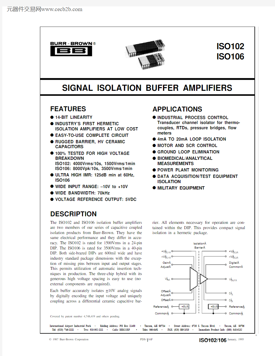
PIN DESCRIPTIONS
±V CC1,
Positive and negative power supply voltages and common (or ground) for the input stage. Common 1 is the analog reference voltage for input Common 1signals. The voltage between Common 1 and Common 2 is the isolation voltage and appears across the internal high voltage barrier.
±V CC2,Positive and negative power supply voltages and common (or ground) for the output stage. Common 2 is the analog reference voltage for output Common 2signals. The voltage between Common 1 and Common 2 is the isolation voltage and appears across the internal high voltage barrier.
V IN Signal input pin. Input impedance is typically 100k ?. The input range is rated for ±10V. The input level can actually exceed the input stage supplies. Output signal swing is limited only by the output supply voltages.
Gain This pin is an optional signal input. A series 5k ? potentiometer between this pin and the input signal allows a guaranteed ±1.5% gain adjustment Adjust range. When gain adjustment is not required, the Gain Adjust should be left open. Figure 4 illustrates the gain adjustment connection.Reference 1
+5V reference output. This low-drift zener voltage reference is necessary for setting the bipolar offset point of the input stage. This pin must be strapped to either Offset or Offset Adjust to allow the isolation amplifier to function. The reference is often useful for input signal conditioning circuits. See “Effect of Reference Loading on Offset” performance curve for the effect of offset voltage change with reference loading.Reference 1 is identical to, but independent of, Reference 2. This output is short circuit protected.
Reference 2+5V reference output. This reference circuit is identical to, but independent of, Reference 1. It controls the bipolar offset of the output stage through an internal connection. This output is short-circuit protected.
Offset Offset input. This input must be strapped to Reference 1 unless user adjustment of bipolar offset is required.
Offset This pin is for optional offset control. When connected to the Reference 1 pin through a 1k ? potentiometer, ±150mV of adjustment range is Adjust guaranteed. Under this condition, the Offset pin should be connected to the Offset Adjust pin. When offset adjustment is not required, the Offset Adjust pin is left open. See Figure 4.
Digital Digital common or ground. This separate ground carries currents from the digital portions of the output stage circuit. The best grounding practi-Common ces require that digital common current does not flow in analog common connections. Both pins can be tied directly to a ground plane if available.Difference in potentials between the Common 2 and Digital Common pins can be ±1V. See Figure 2.
V OUT
Signal output. Because the isolation amplifier has unity gain, the output signal is ideally identical to the input signal. The output is low impedance and is short-circuit protected. This signal is referenced to Common 2; subsequent circuitry should have a separate “sense” connection to Common 1as well as V OUT .
C 1, C 2
Capacitors for small signal bandwidth control. These pins connect to the internal rolloff frequency controlling nodes of the output low-pass filter.Additional capacitance added to these pins will modify the bandwidth of the buffer. C 2 is always twice the value of C 1. See “Bandwidth Control”performance curve for the relationship between bandwidth and C 1 and C 2. When no connections are made to these pins, the full small-signal bandwidth is maintained. Be sure to shield C 1 and C 2 pins from high electric fields on the PC board. This preserves AC isolation-mode rejection by reducing capacitive coupling effects.
5
?
ISO102/106
TYPICAL PERFORMANCE CURVES
T A = +25°C, V CC = ±15VDC unless otherwise noted.
ISOLATION-MODE REJECTION vs ISOLATION VOLTAGE FREQUENCY
Isolation Voltage Frequency (Hz)
I s o l a t i o n -M o d e R e j e c t i o n (d B )160
140
120
100
80
60 10
1M
100
1k
10k
100k
DYNAMIC RANGE vs BANDWIDTH
Small Signal Bandwidth (Hz)
Bandwidth Control Capacitors (F)
D y n a m i c R a n g e (d B )120
110
100
90
80
70 1
10 100 1k 10k 100k 3μ
300n
30n
3nF
300p
30p
BW — C — 1
ISOLATION LEAKAGE CURRENT vs ISOLATION VOLTAGE FREQUENCY
Isolation Voltage Frequency (Hz)
I s o l a t i o n L e a k a g e C u r r e n t (A )10
1M
10m
1m
100μ
10μ
1μ
100n
100
1k
10k
100k
Isolation Voltage (V)
Rated
1
0.5
–0.5
–1
2
1
0 –1 –2 Gain
Offset
T = T to T MIN MAX
? GAIN ERROR AND ? OFFSET VOLTAGE
vs ISOLATION VOLTAGE
G a i n E r r o r (%)? ? O f f s e t V o l t a g e (m V )BANDWIDTH CONTROL
C 1 (F)
S m a l l S i g n a l B a n d w i d t h (H z )
1M
100k
10k 1k 100
10 13p
30p
300p
3n 30n
300n 3μ
POWER DISSIPATION vs TEMPERATURE
Ambient Temperature (°C)
M a x i m u m P o w e r D i s s i p a t i o n (W )
1.6
1.4
1.2
1
0.8
0M a x i m u m P o w e r S u p p l i e s (V )
±20
±15
±10
6
?
ISO102/106
TYPICAL PERFORMANCE CURVES (CONT)
T A = +25°C, V CC = ±15VDC unless otherwise noted.
LARGE SIGNAL TRANSIENT RESPONSE
Time (μs)
100
200 300
400
15 10
5 0 –5 –10 –15
O u t p u t V o l t a g e (V )
TOTAL HARMONIC DISTORTION
Frequency (Hz)
100
1k 10k
100k
T H D + N o i s e (%)10
1
0.1
0 RECOMMENDED RANGE OF ISOLATION VOLTAGE
Isolation Voltage Frequency (Hz)
1k
10k
100k
1M
10k M a x i m u m I s o l a t i o n V o l t a g e (V p k )1k
100
10 2k 5k
GAIN/PHASE vs FREQUENCY
10
100
1k
10k
100k
Frequency (Hz)
S m a l l S i g n a l G a i n (d B )6
–6
–12
–18
90
–90
–180
–270
P h a s e S h i f t (d e g r e e s )
OUTPUT SPECTRAL NOISE DENSITY
40 35 30 25 20 15 10 5 0 S p e c t r a l N o i s e D e n s i t y (d B H z )10μV / H z 0
10
20 30 40 50 Frequency (kHz) N: 128 : 125Hz FS: –47dBV
β GAIN FLATNESS vs FREQUENCY
0 1 2 3 4 5 6 7 8
Frequency (kHz)
L a r g e S i g n a l G a i n (d B )0.03
0.02 0.01 0 –0.01 –0.02 –0.03
7
?
ISO102/106
TYPICAL PERFORMANCE CURVES (CONT)
T A = +25°C, V CC = ±15VDC unless otherwise noted.
FIGURE 1. Simplified Diagram of ISO102 and ISO106.
THEORY OF OPERATION
The ISO102 and ISO106 have no galvanic connection be-tween the input and output. The analog input signal refer-enced to the input common is accurately duplicated at the output referenced to the output common. Because the barrier information is digital, potentials between the two commons can assume a wide range of voltages and frequencies with-out influencing the output signal. Signal information re-mains undisturbed until the slew rate of the barrier voltage exceeds 100V/μs. The isolation amplifier’s ability to reject fast dV/dt changes between the two grounds is specified as transient immunity. The amplifier is protected from damage for slew rates up to 100,000V/μs.
A simplified diagram of the ISO102 and ISO106 is shown in Figure 1. The design consists of an input voltage-controlled oscillator (VCO) also known as a voltage-to-frequency con-verter (VFC), differential capacitors, and output phase lock loop (PLL). The input VCO drives digital levels directly into the two 3pF barrier capacitors. The digital signal is fre-quency modulated and appears differentially across the bar-rier, while the externally applied isolation voltage appears common-mode.
EFFECT OF REFERENCE LOADING ON OFFSET
Voltage Reference Load (mA)
1
2
50
–50
O u t p u t O f f s e t (m V )0.01
0.005
–0.005
–0.01
ISO102B TYPICAL LINEARITY
–10
0 10
V OUT = V IN (V)
N o n l i n e a r i t y (%)5
–5
8
?
ISO102/106
A sense amplifier detects only the differential information.The output stage decodes the frequency modulated signal by the means of a PLL. The feedback of the PLL employs a second VCO that is identical to the encoder VCO. The PLL forces the second VCO to operate at the same frequency (and phase) as the encoder VCO; therefore, the two VCOs have the same input voltage. The input voltage of the decoder VCO serves as the isolation buffer’s output signal after passing through a 100kHz second-order active filter.For a more detailed description of the internal operation of the ISO102 and ISO106, refer to Proceedings of the 1987International Symposium on Microelectronics, pages 202-206.
ABOUT THE BARRIER
For any isolation product, barrier composition is of para-mount importance in achieving high reliability. Both the ISO102 and ISO106 utilize two 3pF high voltage ceramic coupling capacitors. They are constructed of tungsten thick film deposited in a spiral pattern on a ceramic substrate.Capacitor plates are buried in the package, making the barrier very rugged and hermetically sealed. Capacitance results from the fringing electric fields of adjacent metal runs. Dielectric strength exceeds 10kV and resistance is typically 1014?. Input and output circuitry are contained in separate solder-sealed cavities, resulting in the industry’s first fully hermetic hybrid isolation amplifier.
FIGURE 3. Technique for Wiring Analog and Digital Com-mons Together.
FIGURE 2. Power Supply and Signal Connection.
The ISO102 and ISO106 are designed to be free from partial discharge at rated voltages. Partial discharge is a form of localized breakdown that degrades the barrier over time.Since it does not bridge the space across the barrier, it is difficult to detect. Both isolation amplifiers have been exten-
sively evaluated at high temperature and high voltage.POWER SUPPLY AND SIGNAL CONNECTIONS Figure 2 shows the proper power supply and signal connec-tions. Each supply should be AC-bypassed to Analog Com-mon with 0.1μF ceramic capacitors as close to the amplifier as possible. Short leads will minimize lead inductance. A ground plane will also reduce noise problems. Signal com-mon lines should tie directly to the common pin even if a low impedance ground plane is used. Refer to Digital Com-mon in the Pin Descriptions table.
To avoid gain and isolation-mode rejection (IMR) errors introduced by the external circuit, connect grounds as indi-cated, being sure to minimize ground resistance. Any ca-pacitance across the barrier will increase AC leakage current and may degrade high frequency IMR. The schematic in Figure 3 shows the proper technique for wiring analog and digital commons together.
DISCUSSION OF SPECIFICATIONS
The IS0102 and IS0106 are unity gain buffer isolation amplifiers primarily intended for high level input voltages on the order of 1V to 10V. They may be preceded by operational, differential, or instrumentation amplifiers that precondition a low level signal on the order of millivolts and translate it to a high level.
9
?
ISO102/106
noise power varies with the square root of the bandwidth of
the buffer. It is recommended that the bandwidth be reduced to about twice the maximum signal bandwidth for optimum dynamic range as shown in the “Dynamic Range vs Band-width” performance curve. The output spectral noise density measurement is displayed in the “Output Spectral Noise Density” performance curve. The noise is flat to within 5dB Hz between 0.1Hz to 70kHz.
The overall AC gain of the buffer amplifiers is shown in two performance curves: “Gain Flatness vs Frequency” and “Gain/Phase vs Frequency.” Note that with C 1 = 100pF and C 2 = 200pF, the AC gain remains flat within ±0.01dB up to 7kHz. The total harmonic distortion for large-signal sine wave outputs is plotted in the “Total Harmonic Distortion”performance curve. The phase-lock-loop displays slightly nonuniform rise and fall edges under maximum slew condi-tions. Reducing the output filter bandwidth to below 70kHz smoothes the output signal and eliminates any overshoot.See the “Large Signal Transient Response” performance curve.
OPTIONAL OFFSET AND GAIN ADJUSTMENT In many applications the factory-trimmed offset is adequate.For situations where reduced or modified gain and offset are required, adjustment of each is easy. The addition of two potentiometers as shown in Figure 4 provides for a two step calibration.
Offset should be adjusted first. Gain adjustment does not interfere with offset. The potentiometer’s TCR adds only 2% to overall temperature drift. The offset and gain adjust-ment procedures are as follows:
1. Set V IN to 0V and adjust R 1 to desired offset at the output.
2. Set V IN to full scale (not zero). Adjust R 2 for desired gain.
ISOLATION-MODE REJECTION
The IS0102 and IS0106 provide exceptionally high isola-tion-mode rejection over a wide range of isolation-mode voltages and frequencies. The typical performance curves should be used to insure operation within the recommended range. The maximum barrier voltage allowed decreases as the frequency of the voltage increases. As with all isolation amplifiers, a change of voltage across the barrier will induce leakage current across the barrier. In the case of the IS0102and IS0106, there exists a threshold of leakage current through the signal capacitors that can cause over-drive of the decoder’s sense amplifier. This occurs when the slew rate of the isolation voltage reaches 100V/μs. The output will recover in about 50μs from transients exceeding 100V/μs.The first two performance curves indicate the expected isolation-mode rejection over a wide range of isolation voltage frequencies. Also plotted is the typical leakage current across the barrier at 240Vrms. The majority of the leakage current is between the input common pin and the output digital ground pin.
The IS0102 and IS0106 are intended to be continuously operated with fully rated isolation voltage and temperature without significant drift of gain and offset. See the “Gain Error/Offset Isolation Voltage” performance curve for changes in gain and offset with isolation voltage.SUPPLY AND TEMPERATURE RANGE
The IS0102 and IS0106 are rated for +15V supplies; how-ever, they are guaranteed to operate from ±10V to ±20V.Performance is also rated for an ambient temperature range of –25°C to +85°C. For operation outside this temperature range, refer to the “Power Dissipation vs Temperature”performance curve to establish the maximum allowed sup-ply voltage. Supply currents are fairly insensitive to changes in supply voltage or temperature. Therefore, the maximum current limits can be used in computing the maximum junction temperature under nonrated conditions.
OPTIONAL BANDWIDTH CONTROL
The following discussion relates optimum dynamic range performance to bandwidth, noise, and settling time.
The outputs of the IS0102 and IS0106 are the outputs of a second-order low-pass Butterworth filter. Its low impedance output is rated for ±5mA drive and ±12V range with 10,000pF loads. The closed-loop bandwidth of the PLL is 70kHz,while the output filter is internally set at 100kHz. The output filter lowers the residual voltage of the barrier FM signal to below the noise floor of the output signal.
Two pins are available for optional modification of the filter’s bandwidth. Only two capacitors are required. The “Bandwidth Control” performance curve gives the value of C 1 (C 2 is equal to twice C 1) for the desired bandwidth. Figure 4 illustrates the optional connection of both capacitors.A tradeoff can be achieved between the required signal bandwidth and system dynamic range. The noise floor of the output limits the dynamic range of the output signal. The
FIGURE 4. Optional Gain Adjust, Offset Adjust, and Band-width Control.
10
?
ISO102/106
PRINTED CIRCUIT BOARD LAYOUT
The distance across the isolation barrier, between external components, and conductor patterns, should be maximized to reduce leakage and arcing at high voltages. Good layout techniques that reduce stray capacitance will assure low leakage current and high AC IMR. For some applications,applying conformal coating compound such as urethane is useful in maintaining good performance. This is especially true where dirt, grease or moisture can collect on the PC board surface, component surface, or component pins. Fol-lowing this industry-accepted practice will give best results,particularly when circuits are operated or tested in a mois-ture-condensing environment. Optimum coating can be achieved by administering urethane under vacuum condi-tions. This allows complete coverage of all areas. Grounded rings around the C l and C 2 contacts on the board greatly reduce high voltage electric fields at these pins.
APPLICATIONS
The ISO102 and ISO106 isolation amplifiers are used in
three categories of applications:
1.accurate isolation of signals from high voltage ground potentials,
2.accurate isolation of signals from severe ground noise,and
3.fault protection from high voltages in analog measure-ment systems.Figures 5 through 15 show a variety of application circuits.Additional discussion of applications can be found in the December 11, 1986 issue of Electronic Design, pages 91-96.
FIGURE 5. Isolated Power Current Monitor for Motor Cir-cuit. (The ISO102 allows reliable, safe measure-ment at high voltages.)
FIGURE 6. Isolated Power Line Monitor (0.5μA leakage
current at 120Vrms).
FIGURE 7. Battery Monitor for High Voltage Charging
Circuit.
11
?
ISO102/106
FIGURE 11. Low Cost Eight-Channel Isolation Amplifier Block with Channel-to-Channel Isolation.
FIGURE 8. Isolated RTD Temperature Amplifier.
FIGURE 10. Isolation Amplifier with Isolated Bipolar Input
Reference.
FIGURE 9. Programmable-Gain Isolation Channel with Gains
of 1, 10, and 100.
12
?
ISO102/106
FIGURE 12. Thermocouple Amplifier with Ground Loop Elimination, Cold Junction Compensation, and Upscale Burn-out.
FIGURE 13. Remote Isolated Thermocouple Transmitter with Cold Junction Compensation.
13
?
ISO102/106
FIGURE 15. Right-Leg-Driven ECG Amplifier (with defibrillator protection and calibrator).
FIGURE 14. Isolated Instrumentation Amplifier for 300? Bridge. (Reference voltage from isolation amplifier is used to excite
bridge.)
14
?
ISO102/106
AN ERROR ANALYSIS OF THE IS0102 IN A SMALL SIGNAL MEASURING APPLICATION High accuracy measurements of low-level signals in the presence of high isolation mode voltages can be difficult due to the errors of the isolation amplifiers themselves.This error analysis shows that when a low drift operational amplifier is used to preamplify the low-level source signal,a low cost, simple and accurate solution is possible.In the circuit shown in Figure 16, a 50mV shunt is used to measure the current in a 500VDC motor. The OPA27amplifies the 50mV by 200 x to 10V full scale. The output of the OPA27 is fed to the input of the IS0102, which is a unity-gain isolation amplifier. The 5k ? and 1k ? potentiom-eters connected to the IS0102 are used to adjust the gain and offset errors to zero as described in Discussion of Specifica-tions.
Some Observations
The total errors of the op amp and the ISO amp combined are approximately 0.11% of full-scale range (see Figure 17). If the op amp had not been used to preamplify the signal, the errors would have been 2.6% of FSR. Clearly, the small cost of adding the op amp buys a large performance improve-ment. Optimum performance, therefore, is obtained when the full ±10V range of the IS0102/106 is utilized.The rms noise of the IS0102 with a 120Hz bandwidth is only 0.18mVrms, which is only 0.0018% of the 10V full scale output. Therefore, even though the 16μV/ √Hz noise spectral density specification may appear large compared to other isolation amplifiers, it does not turn out to be a significant error term. It is worth noting that even if the bandwidth is increased to 10kHz, the noise of the iso amp would only contribute 0.016%FSR error.
FIGURE 16. 50mV Shunt Measures Current in a 500VDC Motor.
15
?
ISO102/106
The Errors of the Op Amp at 25°C (Referred to Input, RTI)
V E (OPA) = V D
1 – 1 + 1 + V OS (1 + R 1/R F ) + I B R 1 + P.S.R. + Noise
V E (OPA) = Total Op Amp Error (RTI)
V D = Differential Voltage (Full Scale) Across Shunt
1 – 1 + 1 = Gain Error Due to Finite Open Loop Gain
β = Feedback Factor
A VOL = Open Loop Gain at Signal Frequency V OS = Input Offset Voltage I
B = Input Bias Current
P.S.R. = Power Supply Rejection (μV/V) [Assuming a 5% change with ±15V supplies. Total error is twice that due to one supply.]Noise = 5nV/ Hz (for 1k ? source resistance and 1kHz bandwidth)ERROR (OPA) (RTI)GAIN ERROR OFFSET
P.S.R.
NOISE V E (OPA)
=50mV 1 – 1 + 1
{0.025mV (1 + 1/200) + 40 x 10–9 x 103}
(20μV/V x 0.75V x 2){5nV √120 (nVrms)}=
0.01mV (0.0251mV + 0.04mV)+0.03mV +0.055 x 10⁻³mVrms Error as % of FSR =
0.02%
+
(0.05% + 0.08%)
+
0.06%
+
0.00011%
After Nulling
=0.01mV +
(0mV + 0mV)
+
0.03mV
+0.055 x 10⁻³mVrms
=
0.10mV Error as % of FSR*
=0.02%+
(0% + 0%)
+
0.06%
+
0.00011%
=
0.08% of 50mV
*FSR = Full-Scale Range. 50mV at input to op amp, or 10V at input (and output) of ISO amp.
The Errors of the Iso Amp at 25°C (RTI)
V E (ISO) = 1/200 (V ISO /IMR + V OS + G.E. + Nonlinearity + P.S.R. + Noise)V E (ISO) = Total ISO Amp Error IMR = Isolation Mode Rejection V OS = Input Offset Voltage
V ISO = V IMV = Isolation Voltage = Isolation Mode Voltage G.E. = Gain Error (% of FSR)
Nonlinearity = Peak-to-peak deviation of output voltage from best-fit straight line. It is expressed as ratio based on full-scale range.P.S.R. = Change in V OS /10V x Supply Change
Noise = Spectral noise density x √bandwidth. It is recommended that bandwidth be limited to twice maximum signal bandwidth for optimum dynamic range.ERROR (ISO) (RTI)IMR
V OS G.E.
NONLINEARITY
P.S.R.
NOISE V E (ISO)
=1/200 { 500VDC/140dB
+70mV +20V x 0.25/100+0.003/100 x 20V
1.4mV x 0.75V x 2+16μV √120 (rms) }
=
1/200 { 0.05mV
+70mV +50mV +0.6mV + 2.1mV +0.175mVrms }Error as % of FSR =0.0005%
+
0.7%
+
0.5%
+
0.006%
+
0.021%
+
0.00175%
After Nulling V E (ISO)
=1/200 { 0.05mV +
0mV
+
0mV
+
0.6mV
+
2.1mV
+
0.175mVrms }
=1/200 (3.0mV)=
0.03mV Error as % of FSR =
0.0005%+
0%
+
0%
+
0.006%
+
0.021%
+
0.00175%
=
0.03% of 50mV
Total Error
=V E (OPA)+V E (ISO)=0.10mV +
0.03mV =0.08% of 50mV +0.03% of 50mV
=
0.11% of 50mV
{
}
β A VOL
{
}
β A VOL
{ }
106/200
FIGURE 17. Op Amp and Iso Amp Error Analysis.
1
1
1