UT912E-S20-R中文资料
UNISONIC TECHNOLOGIES CO.,
UT912E CMOS IC
ENCODER FOR REMOTE CONTROLLER
DESCRIPTION
The UTC UT912E of CMOS LSIs for remote control system applications is capable of encoding information which consists of N address bits and 12-N data bits. Each address/data input can be set to one of the two logic states. The programmed addresses/data are transmitted together with the header bits by a RF or an infrared transmission medium upon receipt of a trigger signal.
FEATURES
* Operating voltage: 2.4V ~ 12V
* Low power and high noise immunity CMOS technology
* Low standby current (0.1μA (typ.) at V DD=5V)
* Minimum transmission word (Four words)
* Built-in oscillator needs only 5% resistor
* Data code has positive polarity
* Minimal external components
*Pb-free plating product number: UT912EL
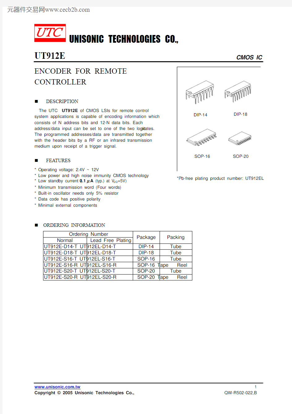
ORDERING INFORMATION
Ordering Number
Normal Lead Free Plating
Package Packing UT912E-D14-T UT912EL-D14-T DIP-14 Tube UT912E-D18-T UT912EL-D18-T DIP-18 Tube UT912E-S16-T UT912EL-S16-T SOP-16 Tube UT912E-S16-R UT912EL-S16-R SOP-16 Tape
Reel UT912E-S20-T UT912EL-S20-T SOP-20 Tube UT912E-S20-R UT912EL-S20-R SOP-20 Tape
Reel
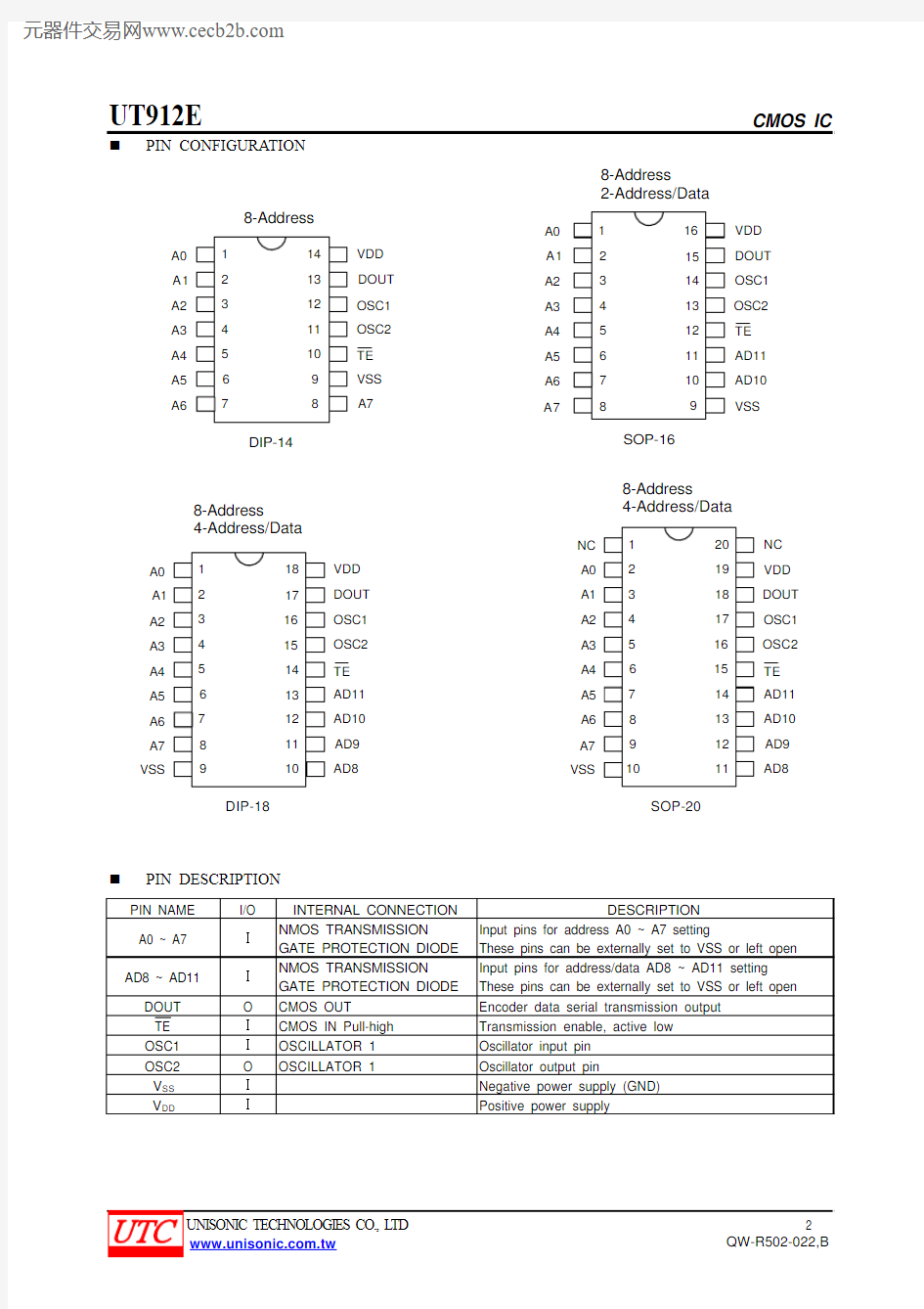
PIN CONFIGURATION
VDD DOUT OSC1OSC2TE VSS A7
A0A1A2A3A4A5
A6
VDD DOUT OSC1OSC2TE AD11AD10A0A1A2A3A4A5A6DIP-14
VSS
A7
SOP-16
8-Address
8-Address
2-Address/Data
VDD DOUT OSC1OSC2TE AD11AD10A0A1A2A3A4A5A6VSS
A7DIP-18
8-Address
4-Address/Data
AD9AD8
NC DOUT OSC1OSC2TE AD11AD10A0A1A2A3A4A5A6VSS
A7SOP-20
8-Address
4-Address/Data
AD9AD8
NC
VDD
PIN DESCRIPTION
BLOCK DIAGRAM
DOUT
ABSOLUTE MAXIMUM RATINGS (Ta=25℃)
PARAMETER SYMBOL RATINGS UNIT Supply Voltage V DD-0.3 ~ +13 V
Input Voltage V IN Vss-0.3 ~ V DD+0.3 V Operating Temperature T OPR0 ~ +70℃
Storage Temperature T STG-40 ~ +150 ℃
ELECTRICAL CHARACTERISTICS (Ta=25℃, unless otherwise specified.)
OPERATION FLOWCHART
■ FUNCTIONAL DESCRIPTION
Operation
The UTC UT912E start a cycle of 4-words transmission upon receipt of a transmission enable (TE). A completed cycle is showed as below. This cycle will repeat itself as long as the transmission enable is held low. While the transmission enable returns high the encoder output completes its final cycle and then stops.
Address/data bit waveform
Each programmable address/data pin can be externally set to one of the following two logic states as shown below.
fosc "One""Zero"
Address/data programming (preset)
The status of each address/data pin can be individually pre-set to logic ”high” or ”low”. If a transmission-enable signal is applied, the encoder scans and transmits the status of the 12 bits of address/data serially in the order A0 to AD11. During information transmission these bits are transmitted with a preceding synchronization bit. If the trigger signal is not applied, the chip enters the standby mode and consumes a reduced current of less than 1μA for a supply voltage of 5V.
The following figure shows an application using the UTC UT912E :
SS
Transmitted information:
A0 A1 A2 A3 A4 A5 A6 A7 AD8AD9AD10 AD11 Pilot & Sync. 1 0 1 0 0 0 1 1 1 1 1 0
Address/Data sequence
The following provides the address/data sequence table for various models of the UTC UT912E encoders. The correct device should be selected according to the individual address and data requirements.
Bits 0 1 2 3 4 5 6 7 8 9 10 11 Address/
Date A0 A1 A2 A3 A4A5A6A7AD8AD9AD10
AD11
.
TYPICAL APPLICATION CIRCUIT
APPROXIMATE INTERNAL CONNECTIONS
OSC1
EN CMOS OUT
CMOS IN NMOS
OSCILLATOR FREQUENCY VS SUPPLY VOLTAGE
V DD (V DC )Unit:V
1.00
2.00
3.00
4.00
5.00
6.00
7.00Fosc unit:KHZ
)
The recommended oscillator frequency is f OSCD (decoder) ≌ 50f OSCE (UT912E encoder)