1-Outstanding gas-sensing performance of graphene-SnO2 Schottky junction

Outstanding gas-sensing performance of graphene/SnO2 nanowire Schottky junctions Vu Van Quang, Nguyen Van Dung, Ngo Sy Trong, Nguyen Duc Hoa, Nguyen Van Duy, and Nguyen Van Hieu
Citation: Applied Physics Letters 105, 013107 (2014); doi: 10.1063/1.4887486
View online: https://www.360docs.net/doc/5a12230130.html,/10.1063/1.4887486
View Table of Contents: https://www.360docs.net/doc/5a12230130.html,/content/aip/journal/apl/105/1?ver=pdfcov
Published by the AIP Publishing
Articles you may be interested in
Influence of in-plane and bridging oxygen vacancies of SnO2 nanostructures on CH4 sensing at low operating temperatures
Appl. Phys. Lett. 105, 243102 (2014); 10.1063/1.4904457
Detection of organic vapors by graphene films functionalized with metallic nanoparticles
J. Appl. Phys. 112, 114326 (2012); 10.1063/1.4768724
Schottky barriers measurements through Arrhenius plots in gas sensors based on semiconductor films
AIP Advances 2, 032138 (2012); 10.1063/1.4746417
Adsorption kinetics of ammonia sensing by graphene films decorated with platinum nanoparticles
J. Appl. Phys. 111, 094317 (2012); 10.1063/1.4714552
ZnO nanowire field-effect transistor and oxygen sensing property
Appl. Phys. Lett. 85, 5923 (2004); 10.1063/1.1836870
Outstanding gas-sensing performance of graphene/SnO 2nanowire Schottky junctions
Vu Van Quang,Nguyen Van Dung,Ngo Sy Trong,Nguyen Duc Hoa,a)Nguyen Van Duy,and Nguyen Van Hieu a)
International Training Institute for Materials Science (ITIMS),Hanoi University of Science and Technology (HUST),Dai Co Viet Road,Hanoi,Viet Nam
(Received 21May 2014;accepted 26June 2014;published online 9July 2014)
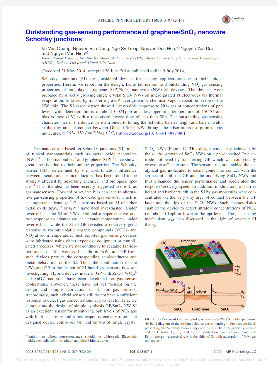
Schottky junctions (SJ)are considered devices for sensing applications due to their unique properties.Herein,we report on the design,facile fabrication,and outstanding NO 2gas sensing properties of monolayer graphene (GP)/SnO 2nanowire (NW)SJ devices.The devices were prepared by directly growing single crystal SnO 2NWs on interdigitated Pt electrodes via thermal evaporation,followed by transferring a GP layer grown by chemical vapor deposition on top of the NW chip.The SJ-based sensor showed a reversible response to NO 2gas at concentrations of ppb levels with detection limits of about 0.024ppb at a low operating temperature of 150 C and bias voltage (1V)with a response/recovery time of less than 50s.The outstanding gas-sensing characteristics of the device were attributed to tuning the Schottky barrier height and barrier width at the tiny area of contact between GP and SnO 2NW through the adsorption/desorption of gas
molecules.V
C 2014AIP Publishing LLC .[https://www.360docs.net/doc/5a12230130.html,/10.1063/1.4887486]Gas nanosensors based on Schottky junctions (SJ),made
of typical nanomaterials such as metal oxide nanowires (NWs),1carbon nanotubes,2and graphene (GP),3have shown great promise due to their unique properties.The Schottky barrier (SB),determined by the work-function difference between metals and semiconductors,has been found to be strongly affected by adsorbing chemical and biological spe-cies.4Thus,the idea has been recently suggested to use SJ as gas nanosensors.Forward or reverse bias can lead to alterna-tive gas-sensing properties of SJ-based gas sensors,which is an important advantage.5Gas sensors based on SJ of either metal oxide NWs 1,5or GP 3,6have been investigated.Under reverse bias,the SJ of NWs exhibited a supersensitive and fast response to ethanol gas at elevated temperatures under reverse bias,while the SJ of GP revealed a relatively good response to various volatile organic compounds (VOCs)and NO 2at room temperature.Such reported gas sensing devices were fabricated using either expensive equipment or compli-cated processes,which are not conducive to scalable fabrica-tion and cost effectiveness.In addition,NWs and GP from such devices provide the corresponding semiconductor and metal behaviors for the SJ.Thus,the combination of the NWs and GP in the design of SJ-based gas sensors is worth investigating.Hybrid devices made of GP with ZnO,7WO 3,8and SnO 29nanorods have been developed for gas sensor applications.However,these have not yet focused on the design and simple fabrication of SJ for gas sensors.Accordingly,such hybrid sensors still do not have a suf?cient response to detect gas concentrations at ppb levels.Here,we demonstrate the design of simple synthesis GP/SnO 2NW SJ as an excellent sensor for monitoring ppb levels of NO 2gas with high sensitivity and a fast response/recovery time.The designed device comprises GP laid on top of single crystal
SnO 2NWs (Figure 1).This design was easily achieved by the in situ growth of SnO 2NWs on a pre-deposited Pt elec-trode,followed by transferring GP which was catalytically grown on a Cu substrate.The sensor structure enabled the an-alytical gas molecules to easily come into contact with the surface of both the GP and the underlying SnO 2NWs and thus enhanced the sensor performance and accelerated the response/recovery speed.In addition,modulations of barrier height and barrier width in the SJ by gas molecules were con-centrated on the very tiny area of contact between the GP layer and the tips of the SnO 2NWs.Such characteristics enabled the device to detect ultralow concentrations of NO 2,i.e.,about 10ppb or lower to the ppt levels.The gas sensing mechanism was also discussed in the light of reversed SJ
theory.
FIG.1.(a)Design of Graphene/SnO 2nanowires (NWs)Schottky junctions;(b)band diagram of the designed device corresponding to the vacuum level;presenting the Schottky barrier (?b )and built in ?eld (V bi )with graphene and SnO 2NWs.E C ,E V ,and E F are conduction band,valance band,and Fermi energy,respectively.D is the shift of ?b with adsorption of NO 2gas molecules.
a)
Authors to whom correspondence should be addressed.Electronic addresses:ndhoa@https://www.360docs.net/doc/5a12230130.html,.vn and hieu@https://www.360docs.net/doc/5a12230130.html,.vn
0003-6951/2014/105(1)/013107/4/$30.00V
C 2014AIP Publishing LLC 105,013107-1
APPLIED PHYSICS LETTERS 105,013107
(2014)
The single crystal SnO 2NWs were directly grown on interdigitated Pt electrodes.10The GP layer,grown by a chemical vapor deposition method,11was transferred to the top of the as-grown SnO 2NWs using PMMA as the support membrane,as shown in Figure 1(a).The gas-sensing meas-urements were done using a ?ow-through technique,12in which a total ?ow rate of 200SCCM (standard cubic centi-meters per minute)of dry air was used as the reference and carrier gas.The electrical signal was measured by a remotely operated Keithley model 2602source meter using a GPIB (General Purpose Interface Bus)interface.The sensor response was de?ned as S ?R gas /R air ,where R air and R gas are the resistan-ces of the sensor in dry air and the analytical gas,respectively.The NO 2gas concentration was varied from 10to 100ppb by diluting the standard concentration of 100ppm with dry air.
The morphology of the as-prepared GP/SnO 2NW SJ de-vice was characterized by SEM,shown in Figures 2(a)–2(d).The survey morphology involved the Pt-electrodes where the SnO 2NWs grew on the ?ngers [Figure 2(a)].The device had ?ve ?ngers,100l m in diameter and 750l m in length.The gap between the ?ngers was 100l m.This gap was designed to be large enough to ensure that the grown SnO 2NWs could not reach from one ?nger to the others [Figure 2(b)].The suc-cessful preparation of the GP/SnO 2NW SJ device was con-?rmed by enlarged images of a ?nger couple [Figure 2(b)],where it can be seen the SnO 2grew on the Pt electrode as dendritic tips [Figure 2(c)],and the bare SiO 2was coated by the GP layer [Figure 2(d)].As can be seen,the length and density of the SnO 2NWs were suf?cient to prevent contact between GP and the Pt electrodes;thus,the electrical proper-ties of the device were mainly from the SnO 2NWs,the GP/SnO 2NW SJ,and the GP.The details are discussed later
in the section on the electrical properties.Synthesis and char-acterization of monolayer graphene grown on Cu substrate were reported in detail in Ref.11.Herein,the Raman spec-troscopy was used to con?rm the successful coating of gra-phene over the SnO 2NW SJ device,as shown in Figure 2(e).The Raman spectra were recorded for different areas of the device con?guration,as marked by GP/SnO 2and GP/SiO 2in the SEM images [inset,Figure 2(e)].Regardless of the effect of the substrate on the Raman signal,the Raman spectra of GP were similar for different positions,except for the Raman mode of SnO 2at 630cm à1recorded in the GP/SnO 2region;otherwise,the typical active Raman modes of GP appear at $1300cm à1,1584cm à1,and 2700cm à1,belonging to the D-band,G-band,and 2D-band,respectively.The peak at 630cm à1can be assigned to O–Sn–O stretching vibrations of tin oxide.The G-band is the active Raman mode of the in-plane vibrations of sp 2-hybridized carbon atoms close to the U point,whereas the 2D-band is due to the double resonance Raman scattering process,representative of a typical GP monolayer.The relatively weak intensity peak centered at $2450cm à1denoted as G*-band represents for the combina-tion of a transverse optical (TO)and longitudinal acoustic (LA)phonon mode near the K point of graphene,as a result of the double resonance Raman scattering process.13
The electrical and gas-sensing properties of the fabri-cated device investigated by the I-V measurements are shown in Figures 3(a)–3(e).The I-V curves showed the non-linear characteristics of the device,indicating the formation of SJ between GP and SnO 2NWs.In a separate study,Ohmic con-tact was formed between GP and the Pt electrode,and between in situ grown SnO 2NWs and the Pt electrode (data not shown).Thus,the SJ were from the GP and SnO 2NWs.The SnO 2NW had a wide direct bandgap of 3.6eV with
a
FIG.2.SEM images of the fabricated graphene/SnO 2junctions:(a)sensor chip;(b)enlarged image of a ?nger;(c)SnO 2nanowires;(d)monolayer Graphene;(e)Raman spectra of the fabricated Graphene/SnO 2junctions recorded at different positions;Inset showed the optical image of the corre-spondent regions recorded the
Raman.
FIG.3.(a)I-V characteristic,(b)the ratio of I air /I gas of the device measured in air and in NO 2(100ppb)at 150 C,(c)transient response of the sensing device measured at different temperatures and NO 2gas concentrations,(d)gas response (R air /R gas )as a function of NO 2gas concentration,and (e)stability of the device upon ?ve cycles switching on/off from air to NO 2and back to air.
work-function of about 4.5eV,14whereas the work-function of GP was about 4.55eV.15Thus,the junctions were made of the SnO 2n-type semiconductor and the zero bandgap GP layer,which acted as a metal in the device and created the SJ.As a result,the I-V curves of the device showed non-linear characteristics.As can be seen in Figure 3(a),at a given applied voltage,the current measured in air was always higher than the value in NO 2.Based on the structure of the designed sensor,the contributions to the electrical resistance (current)of the device involved (i)the resistance of GP,(ii)the resistance of GP/SnO 2NW junctions,and (iii)the resist-ance of SnO 2NWs.Upon exposure to NO 2,the adsorption of gas molecules could modulate all three factors.The interac-tion between analytical gas molecules and GP was theoreti-cally calculated using the ?rst principles method and has been previously reported.16This computation demonstrated that the electronic properties of GP were strongly dependent on the characteristics of GP and the molecular adsorption con?guration.The charge transfer from pristine GP to adsorbed NO 2molecules was theoretically calculated and varied from 0.099to 0.102electrons,which depended on adsorption sites and orientations.17Practically,we could not simply apply this calculation for the experimental measure-ments because the charge transfer in synthesized GP could be different as a result of boundary defects and surface state modi?cations of the GP.However,in our previous report,upon exposure to 100ppm NO 2at 150 C,a planar type GP-based sensor showed a decrease in resistance of about 0.85-fold (R NO2/R air ?0.85).11This variation is very small compared to the change in the GP/SnO 2SJ device regarding the tested concentration,which was 103times lower.In addi-tion,the planar type GP sensor did not show any response upon exposure to ppb concentrations of NO 2under our study conditions.11Therefore,in the GP/SnO 2NW SJ sensor,the contribution of factor (i)is negligible.Factor (iii),i.e.,the variation in resistance of SnO 2NWs upon exposure to ana-lytic gas,is mainly dependent on the adsorption capability of SnO 2.In a single NW SnO 2sensor,upon exposure to a very high concentration of NO 2(50ppm)the resistance of device increased by only three-fold.18Therefore,in the present study,the response of the device was mainly determined by the modulation of the barrier height and barrier width formed between GP/SnO 2NW SJ,which was caused by gas adsorp-tion.3In a report by Kim et al.,the change in the current of the GP/Si junction was mainly modulated by the adsorption of gas molecules (chemical doping)on the GP,which changed the charge concentration and a shift of the Fermi level,resulting in SB height variation.3According to the thermionic emission theory,the current of an ideal Schottky diode is given by the equation:14I ?I o f exp eeV =k B T Tà1g .However,in a real device,the forward I-V characteristic for V >3k B T/q is represented by I ?I o f exp eeV =nk B T Tg ,where
the ideal parameter n is given by n ?q k B
T e@V
@ln eI TT.The SB height can be approximately evaluated from /b ?k B
T
q ln eAA ?T 2
I o T,where I o is the reverse bias saturation current given by I o ?A ?T 2f exp eàe /b =k B T Tg .Here,A*is the Richardson constant,A is the SJ area,T is absolute temperature,k B is the Boltzmann constant,e is the electronic charge,and /b is the barrier height.The reverse saturation current I o and ideality factor n can be determined from the intercept and slope of
Ln(I)vs.V plot.The barrier height was calculated to be about 0.739and 0.762eV in air and in 100ppb NO 2,respectively.The calculated barrier heights are comparable with those val-ues of GP/Si junctions reported elsewhere.3However,in our study,the GP/SnO 2NW device had a different design,i.e.,with two oppositely disposed SJ.Therefore,under working condition,the device was considered as being applied a reversed bias voltage.As reported by Hu et al.,the reverse current is very sensitive to the SB height and barrier width,19thus a small variation in SB height and width caused by gas adsorption can signi?cantly change the current.Utilizing this behavior of the SJ,our designed device was effective in the detection of a low concentration of NO 2at the ppb level.In this work,the decrease in the current of the device can be explained by the adsorption of NO 2molecules on the surface of the SnO 2nanowires,which captured electrons and gener-ated further holes in the n-type semiconductor,leading to lower major carrier density near the contact.These behaviors can result in thickening the depletion region and decrease the current.The I air /I gas plot versus the applied voltages of the GP/SnO 2NW device measured at 150 C is shown in Figure 3(b).As can be seen,with an increasing in the applied voltage from 0to 1V,the sensor response (I air /I gas )increased from 0to 3.A further increase of applied voltage to more than 1V led to a decrease in the I air /I gas ratio;thus,the applied voltage of 1V was optimal for the highest response.The decrease in the response with an increase in applied volt-age above 1V can be explained by the fully open SJ,such that the device was simply in serial contact between GP and SnO 2NWs.
The transient resistance over time of the device meas-ured with a bias voltage of 1V at different temperatures and NO 2gas concentration are shown in Figure 3(c).At a rela-tively low working temperature of 100 C,the sensor showed a long response/recovery time (to 10ppb NO 2)of about 116s/114s,respectively.However,the response and recov-ery time decreased to 43s/37s,17s/15s,6s/4s by increasing the working temperature from 150 C to 250 C.The response/recovery time here is much faster compared to other reports.20For instance,as previously reported,11,19the response/recovery time of pristine GP to NO 2is a few min,whereas those values for SnO 2NW are about 600s/300s at 150 C.21Here,the fast response/recovery time,despite the mechanism of adsorption of NO 2molecules on the GP and SnO 2materials,is not different compared to other studies.This is the result of the sensor design by utilizing the proper-ties of the SJ made of GP/SnO 2NWs under reversed bias applied voltage,which are very sensitive to gas adsorption/desorption.The tiny contact area between GP and the tips of the SnO 2NWs is possibly the reason for the enhanced response and recovery speed.
The sensor response as a function of the NO 2concentra-tion measured at different temperatures is shown in Figure 3(d).It was found that the sensor device could detect very low levels of NO 2gas in the range of 10to 250ppb with a linear dependence of the response on the analytical gas concentration.The sensor exhibited the highest response at an operating temperature of 150 C,and a further increase or decrease in the working temperate led to a decrease in the sensor response.This was possibly due to the optimal
adsorption of NO 2gas on the surface of the SnO 2nanowires,which occurred at around 150 C,where the NO 2gas mole-cules interacted directly with the available tin ionic sites,tak-ing electrons from the conduction band of SnO 2to form the NO 2àspecies.10,22It is worth noting that these gas concen-trations were the lowest detectable concentrations that we could measure due to the limits of our experimental setup.We can extrapolate the detection limit (DL)of our sensors from the experimental data.The sensor noise can be calcu-lated using the variation in the gas response at baseline using the root-mean-square deviation (rms).We took 10experi-mental data points at the baseline of the transient response from Figure 3(c)for ?fth polynomial ?tting.The rms noise
was calculated as rms noise ??????????????????
P eS i àS T2
N
q ,where S i is the ex-perimental data points and S is the corresponding value cal-culated from the ?fth polynomial curve-?tting.The rms noise value was calculated to be 0.0007860.00003.According to the IUPAC de?nition,the DL is calculated as DL ppb eT
?3rms noise
slope ,where slope is the slope value of the linear curve-?tting of gas response (S)versus gas concentration (ppb).The DL value was estimated to be about 0.024ppb (or 24ppt)from the slope value of 0.096960.0005,suggesting that the present sensors can be used to detect NO 2gas at ultralow concentrations down to the ppt level.It is worth to note that the most recently report on the NO 2sensor was based on the aligned SnO 2nanowire ?eld effect transistor.23In such report,the sensor could detect NO 2concentration down to 0.2ppb with a relatively long response and recovery time of several minutes under the assistance of the UV illu-mination.However,the sensor tended to decrease its per-formance after few cycles exposure to analytic gas because the sensing signal could not recover to the initial value.
The stability of the sensor measured after ?ve cycles of switching on/off the dry air to NO 2gas and back to dry air is shown in Figure 3(e).In addition,the device did not decrease in performance after six months of storage in a desiccator under laboratory conditions.This indicates that the device is stable for environmental applications.However,the long-term stability of the device under continuous working condi-tions has not yet been studied.The effect of humidity and the selectivity of sensor to other gases also need further study in order to ful?ll the actual applications.
In summary,a GP/SnO 2NW SJ device was designed and fabricated as a NO 2nanosensor.This nanosensor showed outstanding performance, e.g.,high response,ultralow
detection limit (able to detect down to 24ppt),and fast response/recovery time (less 50s)at a relatively low operat-ing temperature (150 C)and bias voltage (1V).The as-obtained gas sensing performance was also brie?y explained by the SB height and barrier width in the reversed bias voltage.
This research was funded by the Vietnam National Foundation for Science and Technology Development (NAFOSTED)under Grant No.103.02-2011.42.N.V.Hieu also acknowledges for the ?nancial support from VLIR-UOS under Research Initiatives’Project ZEIN2012RIP20.
1
T.-Y.Wei,P.-H.Yeh,S.-Y.Lu,and Z.L.Wang,J.Am.Chem.Soc.131,17690(2009).2
J.Suehiro,H.Imakiire,S.Hidaka,W.Ding,G.Zhou,K.Imasaka,and M.Hara,Sens.Actuators,B 114,943(2006).3
H.-Y.Kim,K.Lee,N.McEvoy,C.Yim,and G.S.Duesberg,Nano Lett.13,2182(2013).4
R.T.Tung,Appl.Phys.Rev.1,011304(2014).5
J.Yu,S.J.Ippolito,W.Wlodarski,M.Strano,and K.Kalantar-zadeh,Nanotechnology 21,265502(2010).6
M.Sha?ei,P.G.Spizzirri,R.Arsat,J.Yu,J.du Plessis,S.Dubin,R.B.Kaner,K.Kalantar-zadeh,and W.Wlodarski,J.Phys.Chem.C 114,13796(2010).7
J.Yi,J.M.Lee,and W.Il Park,Sens.Actuators,B 155,264(2011).8
X.An,J.C.Yu,Y.Wang,Y.Hu,X.Yu,and G.Zhang,J.Mater.Chem.22,8525(2012).9
Z.Zhang,R.Zou,G.Song,L.Yu,Z.Chen,and J.Hu,J.Mater.Chem.21,17360(2011).10
D.T.T.Le,N.Duy,H.M.Tan,D.D.Trung,N.N.Trung,P.T.H.Van,N.D.Hoa,and N.Hieu,J.Mater.Sci.48,7253(2013).11
V.Van Quang,N.S.Trong,N.N.Trung,N.D.Hoa,N.Van Duy,and N.Van Hieu,Anal.Lett.47,280(2014).12
N.Van Hieu,P.Thi Hong Van,L.Tien Nhan,N.Van Duy,and N.Duc Hoa,Appl.Phys.Lett.101,253106(2012).13
P.May,https://www.360docs.net/doc/5a12230130.html,zzeri,P.Venezuela,F.Herziger,G.Callsen,J.Reparaz,A.Hoffmann,F.Mauri,and J.Maultzsch,Phys.Rev.B 87,075402(2013).14
S.Gubbala,H.B.Russell,H.Shah,B.Deb,J.Jasinski,H.Rypkema,and M.K.Sunkara,Energy Environ.Sci.2,1302(2009).15
V.Panchal,R.Pearce,R.Yakimova,A.Tzalenchuk,and O.Kazakova,Sci.Rep.3,2597(2013).16
Y.-H.Zhang,Y.-B.Chen,K.-G.Zhou,C.-H.Liu,J.Zeng,H.-L.Zhang,and Y.Peng,Nanotechnology 20,185504(2009).17
O.Leenaerts,B.Partoens,and F.Peeters,Phys.Rev.B 77,125416(2008).18
M.Tonezzer and N.V.Hieu,Sens.Actuators,B 163,146(2012).19
Y.Hu,J.Zhou,P.-H.Yeh,Z.Li,T.-Y.Wei,and Z.L.Wang,Adv.Mater.22,3327(2010).20
F.Schedin,A.K.Geim,S.V.Morozov,E.W.Hill,P.Blake,M.I.Katsnelson,and K.S.Novoselov,Nat.Mater.6,652(2007).21
B.Ruhland,T.Becker,and G.M €u ller,Sens.Actuators,B 50,85(1998).22
A.Sharma,M.Tomar,and V.Gupta,J.Mater.Chem.22,23608(2012).23
X.Wang,N.Aroonyadet,Y.Zhang,M.Mecklenburg,X.Fang,H.Chen,E.Goo,and C.Zhou,Nano Lett.14,3014(2014).