CLC031中文资料

CLC031
SMPTE 292M/259M Digital Video Deserializer /Descrambler with Video and Ancilliary Data FIFOs
General Description
The CLC031SMPTE 292M /259M Digital Video Deserializer/Descrambler with Video and Ancilliary Data FIFOs is a monolithic integrated circuit that deserializes and decodes SMPTE 292M,1.485Gbps (or 1.483Gbps)serial component video data,to 20-bit parallel data with a synchro-nized parallel word-rate clock.It also deserializes and de-codes SMPTE 259M,270Mbps,360Mbps and SMPTE 344M (proposed)540Mbps serial component video data,to 10-bit parallel data.Functions performed by the CLC031include:clock/data recovery from the serial data,serial-to-parallel data conversion,SMPTE standard data de-coding,NRZI-to-NRZ conversion,parallel data clock genera-tion,word framing,CRC and EDH data checking and han-dling,ancilliary data extraction and automatic video format determination.The parallel video output features a variable-depth FIFO which can be adjusted to delay the output data up to 4parallel data clock periods.Ancilliary data may be selectively extracted from the parallel data through the use of masking and control bits in the configuration and control registers and stored in the on-chip FIFO.Reverse LSB dith-ering is also implemented.
The unique multi-functional I/O port of the CLC031provides external access to functions and data stored in the configu-ration and control registers.This feature allows the designer greater flexibility in tailoring the CLC031to the desired ap-plication.The CLC031is auto-configured to a default oper-ating condition at power-on or after a reset command.Sepa-rate power pins for the PLL,deserializer and other functional circuits improve power supply rejection and noise perfor-mance.
The CLC031has a unique Built-In Self-Test (BIST)and video Test Pattern Generator (TPG).The BIST enables com-prehensive testing of the device by the user.The BIST uses the TPG as input data and includes SD and HD component video test patterns,reference black,PLL and EQ pathologi-cals and a 75%saturation,8vertical colour bar pattern,for all implemented rasters.The colour bar pattern has optional transition coding at changes in the chroma and luma bar data.The TPG data is output via the parallel data port.
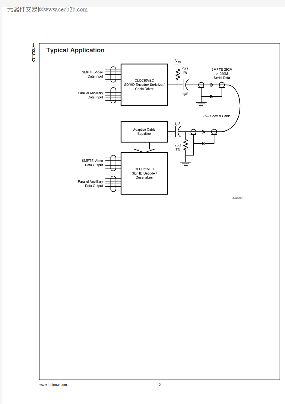
The CLC030,SMPTE 292M /259M Digital Video Serializer with Ancilliary Data FIFO and Integrated Cable Driver,is the ideal complement to the CLC031.
The CLC031’s internal circuitry is powered from +2.5Volts and the I/O circuitry from a +3.3Volt supply.Power dissipa-tion is typically 850mW.The device is packaged in a 64-pin TQFP .
Features
n SDTV/HDTV serial digital video standard compliant n Supports 270Mbps,360Mbps,540Mbps,1.483Gbps and 1.485Gbps serial video data rates with auto-detection
n LSB de-dithering option
n Uses low-cost 27MHz crystal or clock oscillator reference
n Fast VCO lock time:<500μs at 1.485Gbps
n Built-in self-test (BIST)and video test pattern generator (TPG)*
n Automatic EDH/CRC word and flag processing
n Ancilliary data FIFO with extensive packet handling options
n Adjustable,4-deep parallel output video data FIFO n Flexible control and configuration I/O port
n LVCMOS compatible control inputs and clock and data outputs
n LVDS and ECL-compatible,differential,serial inputs n 3.3V I/O power supply and 2.5V logic power supply operation
n Low power:typically 850mW n 64-pin TQFP package
n Commercial temperature range 0?C to +70?C
*Patent applications made or pending.
Applications
n SDTV/HDTV serial-to-parallel digital video interfaces for:—Video editing equipment —VTRs
—Standards converters
—Digital video routers and switchers
—Digital video processing and editing equipment —Video test pattern generators and digital video test equipment
—Video signal generators
Ordering Information
Order Number Package Type NS Package Number
CLC031VEC
64-Pin TQFP
VEC-64A
PRELIMINARY
August 2003
CLC031SMPTE 292M/259M Digital Video Deserializer /Descrambler with Video and Ancilliary Data FIFOs
?2003National Semiconductor Corporation https://www.360docs.net/doc/5e14075958.html,
Typical Application
20020101
C L C 031
https://www.360docs.net/doc/5e14075958.html, 2
CLC031 Block Diagram
20020102
https://www.360docs.net/doc/5e14075958.html,
3
Connection Diagram
20020103
64-Pin TQFP
Order Number CLC031VEC See NS Package Number VEC-64A
C L C 031
https://www.360docs.net/doc/5e14075958.html, 4
Absolute Maximum Ratings(Note1) It is anticipated that this device will not be offered in a military qualified version.If Military/Aerospace speci-fied devices are required,please contact the National Semiconductor Sales Office/Distributors for availability and specifications.
CMOS I/O Supply Voltage
(V DDIO–V SSIO): 4.0V SDI Supply Voltage
(V DDSI–V SSSI): 4.0V Digital Logic Supply Voltage
(V DDD–V SSD): 3.0V PLL Supply Voltage
(V DDPLL–V SSPLL): 3.0V
CMOS Input Voltage (Vi):V SSIO?0.15V to V DDIO+0.15V
CMOS Output Voltage (Vo):V SSIO?0.15V to
V DDIO+0.15V
CMOS Input Current(single input):
Vi=V SSIO?0.15V:?5mA
Vi=V DDIO+0.15V:+5mA
CMOS Output Source/Sink Current:±6mA
I BB Output Current:+300μA
I REF Output Current:+300μA
SDI Input Voltage
(Vi):
V SSSI?0.15V to
V DDSI+0.15V
Package Thermal Resistance
θJA@0LFM Airflow40.1?C/W
θJA@500LFM Airflow24.5?C/W
θJC 5.23?C/W
Storage Temp.Range:?65?C to+150?C
Junction Temperature:+150?C
Lead Temperature(Soldering4
Sec):+260?C
ESD Rating(HBM):>2.5kV
ESD Rating(MM):>250V
Recommended Operating Conditions
Symbol Parameter Conditions Reference Min Typ Max Units V DDIO CMOS I/O Supply Voltage V DDIO?V SSIO
3.150 3.300 3.450V V DDSD SDI Supply Voltage V DDSI?V SSSI
V DDD Digital Logic Supply
Voltage
V DDD–V SSD
2.375 2.500 2.625V
V DDPLL PLL Supply Voltage V DDPLL–V SSPLL
T A Operating Free Air
Temperature
0+70?C
Required Input Conditions
(Note9)
Symbol Parameter Conditions Reference Min Typ Max Units
V IN Input Voltage Range All LVCMOS
Inputs V SSIO V DDIO V
t r,t f Rise Time,Fall Time10%–90% 1.0 1.5 3.0ns
BR SDI Serial Input Data Rate SMPTE259M,Level C
SDI,SDI
270
M BPS SMPTE259M,Level D360
SMPTE344M540
SMPTE292M1,483
SMPTE292M1,485
V CM(SDI)Common Mode Voltage
V IN=100mV
SDI,SDI
V SSSI
+0.05V
V DDSI
?0.05V
V
V IN(SDI)SDI Serial Input Voltage100800880mV
t r,t f Rise Time,Fall Time 20%–80%,SMPTE259M
Data Rates
720800880
ps
20%–80%,SMPTE292M
Data Rates
270
CLC031
https://www.360docs.net/doc/5e14075958.html,
5
Required Input Conditions
(Continued)Symbol Parameter
Conditions
Reference
Min
Typ
Max Units f ACLK Ancilliary /Control Data Clock Frequency A CLK
74.25
MHz DC ACLK
Ancilliary /Control Clock Duty Cycle
45
50
55
%
t r ,t f
Ancilliary /Control Clock and Data Rise Time,Fall Time
10%–90%
1.0 1.5 3.0ns
t S
Setup Time,AD N to A CLK or IO N to A CLK Rising Edge
Control Data Input or I/O Bus Input
IO N ,AD N ,A CLK Timing Diagram
3.0
1.5ns
t H
Hold Time,Rising Edge A CLK to AD N or A CLK to IO N
3.0
1.5ns
R REF Bias Supply Reference Resistor
Tolerance 1%
4.75k ?f EXT CLK External Clock Frequency Ext Clk
?100ppm
27.0
+100ppm
MHz
f XTAL
Crystal Frequency
Figure 6
XTALo,XTALi
DC Electrical Characteristics
Over Supply Voltage and Operating Temperature ranges,unless otherwise specified (Notes 2,3).Symbol Parameter
Conditions
Reference
Min Typ
Max Units V IH Input Voltage High Level All LVCMOS Inputs
2.0V DDIO V V IL Input Voltage Low Level V SSIO
0.8I IH Input Current High Level V IH =V DDIO (Note 8)+85+150μA
I IL Input Current Low Level V IL =V SSIO ?1?20V OH Output Voltage High Level I OH =?2mA All LVCMOS Outputs
2.4 2.7V DDIO V V OL Output Voltage Low Level I OL =+2mA V SSIO
V SSIO +0.3V SSIO +0.5V
V OHV Minimum Dynamic V OH I OH =?2mA (Note 6)V DDIO ?0.5V OLP Maximum Dynamic V OL I OL =+2mA (Note 6)
V SSIO +0.4V SDI Serial Data Input Voltage SDI,SDI
100
800
880
mV P-P I SDI Serial Data Input Current ±1±10
μA V TH Input Thereshold Over VCM range <50
mV
I BB Bias Supply Output Current
R BB =6.19k ?1%188220μA
I REF
Reference Output Current R REF =4.75k ?1%262290I DD (3.3V)Power Supply Current,3.3V Supply,Total 270M BPS Data Rate V DDIO ,V DDSI 31.045.0mA 1,485M BPS Data Rate 35.050.0I DD (2.5V)
Power Supply Current,2.5V Supply,Total
270M BPS Data Rate V DDD ,V DDPLL 76115mA 1,485M BPS Data Rate
210
325
C L C 031
https://www.360docs.net/doc/5e14075958.html, 6
AC Electrical Characteristics
Over Supply Voltage and Operating Temperature ranges,unless otherwise specified(Note3).
Symbol Parameter Conditions Reference Min Typ Max Units Serial Video Data Inputs
BR SDI Serial Input Data Rate
SMPTE259M,Level C
SDI,SDI 270
M BPS
SMPTE259M,Level D360 SMPTE344M540 SMPTE292M1,483 SMPTE292M1,485
t r,t f Rise Time,Fall Time 20%–80%,SMPTE259M
Data Rates
720800880
ps 20%–80%,SMPTE292M
Data Rates
270
Parallel Video Data Outputs
f VCLK Video Output Clock
Frequency
SMPTE259M,270M BPS
V CLK
27.0
MHz
SMPTE267M,360M BPS36.0
SMPTE344M,540M BPS54.0
SMPTE292M,1,483M BPS74.176
SMPTE292M,1,485M BPS74.25
t pd Propagation Delay,Video
Clock to Video Data Valid
50%–50%
V CLK to DV N
Timing Diagram
0.5 2.0ns
t JIT Video Data Output Clock
Jitter
27MHz
V CLK
3.0
ns P-P
36MHz 2.2
54MHz 1.5
74.25MHz 1.0
Parallel Ancilliary/Control Data Inputs,Multi-function Parallel Bus Inputs
f ACLK Ancilliary/Control Data
Clock Frequency
A CLK
74.25MHz
DC A Ancilliary/Control Clock
Duty Cycle
ANC Data clock
(Note7)
455055%
t r,t f Output Rise Time,Fall
Time
10%–90%
IO N,AD N,A CLK
Timing Diagram
1.0 1.5 3.0
ns
t S Setup Time,AD N to A CLK
or IO N to A CLK Rising Edge
Control Data Input or I/O
Bus Input
3.0 1.5
t H Hold Time,Rising Edge
A CLK to AD N or A CLK to
IO N
3.0 1.5
Parallel Ancilliary/Control Data Outputs
t pd Propagation Delay,Clock
to Control Data
50%–50%
A CLK to AD N
Timing Diagram
8.5
ns
t pd Propagation Delay,Clock
to Ancilliary Data
11.5
Multi-function Parallel I/O Bus
t r,t f Rise Time,Fall Time10%–90%IO0–IO7
Timing Diagram
1.0 1.5 3.0ns
PLL/CDR,Format Detect
t LOCK Lock Detect Time SD Rates(Note5)0.32 1.0
ms HD Rates(Note5)0.26 1.0
t FORMAT Format Detect Time All Rates20 Note1:“Absolute Maximum Ratings”are those parameter values beyond which the life and operation of the device cannot be guaranteed.The stating herein of these maximums shall not be construed to imply that the device can or should be operated at or beyond these values.The table of“Electrical Characteristics”
specifies acceptable device operating conditions.
Note2:Current flow into device pins is defined as positive.Current flow out of device pins is defined as negative.All voltages are referenced to V SSIO=V SSD= V SSSI=0V.
CLC031
https://www.360docs.net/doc/5e14075958.html,
7
AC Electrical Characteristics
(Continued)
Note 3:Typical values are stated for V DDIO =V DDSI =+3.3V,V DDD =V DDPLL =+2.5V and T A =+25?C.
Note 4:Spec.is guaranteed by design.
Note 5:Measured from rising-edge of first SDI cycle until Lock Detect bit goes high (true).Lock time includes CDR phase acquisition time plus PLL lock time.Note 6:V OHV and V OLP are measured with respect to reference ground.V OLP is the peak output LOW voltage or ground bounce that may occur under dynamic simultaneous output switching conditions.V OHV is the lowest output HIGH voltage or output droop that may occur under dynamic simultaneous output switching conditions.
Note 7:When used to clock control data into or from the CLC031,the duty cycle restriction does not apply.Note 8:I IH includes static current required by input pull-down devices.
Note 9:Required Input Conditions are the electrical signal conditions or component values which shall be supplied by the circuit in which this device is used in order for it to produce the specified DC and AC electrical output characteristics.
Note 10:Functional and certain other parametric tests utilize a CLC030as the input source to the SDI inputs of the CLC031.The CLC030is DC coupled to the inputs of the CLC031.Typical V IN =800mV,V CM =2.9V.
Test Loads
20020104
C L C 031
https://www.360docs.net/doc/5e14075958.html, 8
CLC031 Test Circuit
20020107
https://www.360docs.net/doc/5e14075958.html,
9
Timing Diagram
20020108
Device Operation
Introduction
The CLC031SMPTE 292M/259M Digital Video Deserializer/Decoder is used in digital video signal origination and desti-nation equipment:cameras,video tape recorders,telecines,editors,standards converters,video test and other equip-ment.It decodes and converts serial SDTV or HDTV com-ponent digital video signals into parallel format.The CLC031decoder/deserializer processes serial digital video (SDV)signals conforming to SMPTE 259M,SMPTE 344M (pro-posed)or SMPTE 292M and operates at serial data rates of 270Mbps,360Mbps,540Mbps, 1.483Gbps and 1.485Gbps.Corresponding parallel output data rates are 27.0MHz,36.0MHz,54.0MHz,74.176MHz and 74.25MHz.The CLC031accepts ECL or LVDS serial data input signals.Outputs signals are compatible with LVCMOS logic devices.Note:In the following explanations,these logical equiva-lences are observed:ON ≡Enabled ≡Set ≡True ≡Logic_1and OFF ≡Disabled ≡Reset ≡False ≡Logic_0.
VIDEO DATA PATH
The Serial Data Inputs (SDI)accept serial video data at SMPTE 259M standard definition,SMPTE 344M (proposed)or SMPTE 292M high-definition data rates.These inputs accept standard ECL or LVDS signal levels and may be used single-ended or differentially.Inputs may be DC or AC coupled,as required,to devices and circuits supplying the data.Recommended operating conditions and all input DC and AC voltage and current specifications shall be observed when designing the input coupling circuits.
For convenience,a reference bias source,pin name R REF ,sets the reference current available from the input bias source,pin name R BB .The recommended nominal value of R REF is 4.75k ?,1%.R BB is provided so that the SDI inputs may be supplied DC bias voltage via external resistors when the inputs are AC-coupled.The bias source should be loaded with a resistance to the V SS supply.The source current available at R BB is 200μA.Figure 1shows a typical input biasing scheme using R BB and R REF .
C L C 031
https://www.360docs.net/doc/5e14075958.html, 10
Device Operation(Continued)
The SMPTE descrambler receives NRZI serial data,con-verts it to NRZ,then decodes it to either10-bit standard definition or20-bit high definition parallel video data using the reverse polynomial X9+X4+1as specified in the respective standard:SMPTE259M,SMPTE344M(pro-posed)or SMPTE292M.The data reception bit order is LSB-first.All data processing is done at the parallel rate. The CLC031incorporates circuitry that implements a method for handling data that has been subjected to LSB dithering.When so enabled,data from the de-scrambler is routed for de-dithering.The De-Dither Enable bit in the VIDEO INFO0control register enables this function.De-dithering of data present in the vertical blanking interval can be selectively enabled by use of the V De-Dither Enable bit in the VIDEO INFO0control register.The initial condition of De-Dither Enable and V De-Dither Enable is OFF.
The descrambler supplies signals to the TRS character de-tector which identifies the presence of the valid video data. The TRS character detector processes the timing refer-ence signals which control raster framing.TRS(sync)char-acters are detected and the video is aligned on word bound-aries.Data is re-synchronized with the parallel word-rate clock.Interraction and operation of the character alignment control signals and indicators Framing Mode,Framing En-able and NSP(New Sync Position)is described later in this datasheet.
The CLC031implements TRS character LSB-clipping as prescribed in ITU-R BT.601.LSB-clipping causes all TRS characters with a value between000h and003h to be forced to000h and all TRS characters with a value between3FCh and3FFh to be forced to3FFh.Clipping is done after de-scrambling and de-dithering.
Once the PLL attains lock,the video format detector pro-cesses the received data to determine the raster character-istics(video data format)and configure the CLC031to handle it.This assures that the parallel output data will be properly formatted,that the correct data rate is selected and that ancilliary data and CRC/EDH data are correctly de-tected and checked.Supported parallel data formats or sub-formats may belong to any one of several component stan-dards:SMPTE125M,SMPTE267M,SMPTE260M,274M, 295M or296M.Refer to Table4for the supported formats. (See also the Application Information section for handling of other raster formats or format extensions developed after this device was designed).The detected video standard information is passed to the device control system and saved in the control registers from whence it may be read by the user.
The CLC031may be configured to operate in a single video format by loading the appropriate FORMAT SET[4:0]control data into the FORMAT0control register.Also,the CLC031 may be configured to handle only the standard-definition data formats by setting the SD ONLY bit or only the high-definition data formats by setting the HD ONLY bit in the FORMAT0control register.When both bits are reset,the default condition,the part automatically detects the data rate and range.
Aligned and de-processed parallel data passes into a variable-depth video FIFO prior to output.Video FIFO depth from0to4registers is set by a3-bit word written into the VIDEO FIFO Depth[2:0]bits in the ANC0control register. The video FIFO permits adjustment of the parallel video data output timing or delay at a parallel word rate.The occurence of corresponding TRS indicator bits,EAV,SAV and NSP,in the control register corresponds to the input register position of the FIFO.This positioning permits a look-ahead function in which the alignment status of the video data can be determined up to four parallel clock periods prior to the appearance of that data at the parallel data output.
The parallel video data is output on DV[19:0].The20-bit parallel video data is organized so that for HDTV data,the upper-order10bits DV[19:10]are luminance(luma)infor-mation and the lower10bits DV[9:0]are colour difference (chroma)information.SDTV data use the lower-order10-bits DV[9:0]for both luma and chroma information.(The SDTV parallel data is also duplicated on DV[19:10]).V CLK is the parallel output word rate clock signal.The frequency of V CLK is appropriate to either the HD or SD data being processed. Data is valid between the falling edges of a V CLK cycle.Data may be clocked into external devices on the rising-edge of V CLK.The DV[19:0]and V CLK signals are LVCMOS-compatible.
20020106
FIGURE1.Optional Input Biasing Scheme
CLC031
https://www.360docs.net/doc/5e14075958.html,
11
Device Operation
(Continued)
ANCILLIARY/CONTROL DATA PATH
The 10-bit Ancilliary and Control Data Port AD[9:0]serves two functions in the CLC031.Ancilliary data from the Ancilliary Data FIFO is output from this port after its recov-ery from the video data stream.The utilization and flow of ancilliary data from the device is managed by a system of control bits,masks and IDs stored in the control data regis-ters.This port also provides read/write access to contents of the configuration and control registers.The signals RD/WR ,ANC/CTRL and A CLK control data flow through the port.Control Data Functions
Control data is input to and output from the CLC031using the lower-order 8bits AD[7:0]of the Ancilliary/Control Data Port.This control data initializes,monitors and controls op-eration of the CLC031.The upper two bits AD[9:8]of the port function as handshaking signals with the device access-ing the port.When either a control register read or write address is being written to the port,AD[9:8]must be driven as 00b (0XXh,where XX are AD[7:0]).When control data is being written to the port,AD[9:8]must be driven as 11b (3XXh,where XX are AD[7:0]).When control data is being read from the port,the CLC031will output AD[9:8]as 10b (2XXh,where XX are output data AD[7:0])and may be ignored by the monitoring system.
Note:After either a manual or power-on reset,A CLK must be toggled three (3)times to complete initiallization of the An-cilliary and Control Data Port .
The sequence of clock and control signals for reading control data from the ancilliary/control data port is shown in Figure 2.Control data read mode is invoked by making the ANC/CTRL input low and the RD/WR input high.The 8-bit ad-dress of the control register set to be accessed is input to the port on bits AD[7:0].To identify the data as an address,AD[9:8]must be driven as 00b.The complete address word will be 0XXh,where 0is AD[9:8]and XX are AD[7:0].The address is captured on the rising edge of A CLK .When control data is being read from the port,the CLC031will output AD[9:8]as 10b (2XXh,where XX are output data AD[7:0])and may be ignored by the monitoring system.Data being output from the selected register is driven by the port immediately following the rising edge of A CLK or when the address signal is removed.For optimum system timing,the signals driving the address to the port should be removed immediately after the address is clocked into the port and
before or simultaneously with the falling edge of A CLK at the end of that address cycle.Output data remains stable until the next rising edge of A CLK and may be written into external devices at any time after the removal of the address signal.This second clock resets the port from drive to receive and readies the port for another access cycle.
Example:Read the Full-field Flags via the AD port.1.Set ANC/CTRL to a logic-low.2.Set RD/WR to a logic-high.
3.Present 001h to AD[9:0]as the register address.
4.Toggle A CLK .
5.Release the bus driving the AD port.
6.Read the data present on the AD port.The Full-field
Flags are bits AD[4:0].
7.Toggle A CLK to release the AD port.
Figure 3shows the sequence of clock and control signals for writing control data to the ancilliary/control data port.The control data write mode is similar to the read mode.Con-trol data write mode is invoked by making the ANC/CTRL input low and the RD/WR input low.The 8-bit address of the control register set to be accessed is input to the port on bits AD[7:0].When a control register write address is being written to the port,AD[9:8]must be driven as 00b (0XXh,where XX are AD[7:0]).The address is captured on the rising edge of A CLK .The address data is removed on the falling edge of A CLK .Next,the control data is presented to the port bits AD[7:0]and written into the selected register on the next rising edge of A CLK .When control data is being written to the port,AD[9:8]must be driven as 11b (3XXh,where XX are AD[7:0]).Control data written into the registers may be read out non-destructively in most cases.
Example:Setup (without enabling)the TPG Mode via the AD port using the 1125line,30frame,74.25MHz,interlaced component (SMPTE 274M)colour bars as test pattern.The TPG may be enabled after setup using the Multi-function I/O port or by the control registers.1.Set ANC/CTRL to a logic-low.2.Set RD/WR to a logic-low.
3.Present 00Dh to AD[9:0]as the Test 0register address.
4.Toggle A CLK .
5.Present 027h to AD[9:0]as the register data.
6.Toggle A CLK .
C L C 031
https://www.360docs.net/doc/5e14075958.html, 12
Device Operation
(Continued)
Ancilliary Data Functions
The CLC031can recover Ancilliary Data from the serial data stream.This ancilliary data and related control charac-ters are defined in the relevant SMPTE standards and may reside in the horizontal and vertical blanking intervals.The data can consist of different types of message packets in-cluding audio data.The serial ancilliary data space must be formatted according to SMPTE 291M.The CLC031sup-ports ancilliary data in the chrominance channel (C’r/C’b)only for high-definition operation.Ancilliary data for standard definition follows the requirements of SMPTE 125M.
The Ancilliary Data FIFO is sized to handle a maximum length ANC data Type 1or Type 2packet without the ANC Flag,259words.Defined in SMPTE 291M,the packet con-sists of the Ancilliary Data Flag,a 3-word Data ID and Data Count,2558-or 10-bit User Data Words and a Checksum.The design of the CLC031Ancilliary Data FIFO also allows storage of up to 8shorter length messages with total length not exceeding 259words including all ID information.Ancil-liary Data is copied from the data stream into the Ancilliary Data FIFO .The parallel ancilliary data will still be present in the parallel chroma output DV[9:0].Ancilliary flag informa-tion is not extracted into the FIFO.
Copying of ANC data from the video data into the FIFO is controlled by the ANC Mask and ANC ID bits in the control registers.A system of flags,ANC FIFO Empty ,ANC FIFO 90%Full ,ANC FIFO Full and ANC FIFO Overrun are used to monitor FIFO status.The details and functions of these and other control words are explained later in this datasheet.
20020109
FIGURE 2.Control Data Read Timing (2read and 1write cycle shown)
20020110
FIGURE 3.Control Data Write Timing
CLC031
https://www.360docs.net/doc/5e14075958.html,
13
Device Operation
(Continued)
Figure 4shows the relationship of clock,data and control signals for reading Ancilliary Data from the port AD[9:0].In ancilliary data read mode,10-bit ancilliary data is routed from the Ancilliary Data FIFO and read from the port AD[9:0]at a rate determined by A CLK .
Ancilliary data read (output)mode is invoked by making the ANC/CTRL input high and the RD/WR input high.Ancilliary Data is clocked from the FIFO on the L-H transition of A CLK .Data may be read from the port on rising edges of A CLK ,after the specified propagation delay,until the FIFO is emp-
tied.Data may only be read from the port when in the ancilliary data mode.Ancilliary data cannot be written to the port.
To conserve power when the ancilliary data function is not being used,the internal Ancilliary Data FIFO clock is dis-abled.This clock must be enabled before ancilliary data may be replicated into the FIFO for output.This internal FIFO clock is controlled by FIFO CLOCK ENABLE ,bit-6of the ANC 5register (address 17h).The default condition of FIFO CLOCK ENABLE is OFF.After enabling the internal FIFO clock by turning this bit ON,A CLK must be toggled three (3)times to propagate the enable to the clock tree.
MULTI-FUNCTION I/O PORT
The multi-function I/O port can be configured to provide immediate access to many control and indicator functions that are stored within the CLC031’s configuration and control registers.The individual pins comprising this port are as-signed as input or output for selected functions stored in the control data registers.
The multi-function I/O port is configured by way of an 8x6-bit register bank consisting of registers I/O pin 0CONFIG through I/O pin 7CONFIG .The contents of these registers determine whether the port bits function as inputs or outputs and to which control function or indicator each port bit is assigned.Port bits may be assigned to access different functions and indicators or any or all port bits may be as-signed to access the same function or indicator (output mode only).The same indicator or function should not be assigned to more than one port bit as an input.Controls and indicators that are accessible by the port and their corre-sponding selection addresses are given in the I/O Pin Con-figuration Register Addresses,Table 6.Table 2gives the control register bit assignments.
Data resulting from device operation will be sent to the selected I/O port bit.This same data is also stored in the configuration and control registers.Mapping the control and indicator functions in this manner means that device opera-tion will be immediately reflected at the I/O port pins thereby ensuring more reliable real-time operation of the device within and by the host system.
When a multifunction I/O port bit is used as input to a control register bit,data must be presented to the I/O port bit and clocked into the register bit using A CLK as shown in Figure 5.Port timing for bit write operations is the same as for the ANC/CTRL port operation.
Example:Program multi-function I/O port bit-0as the CRC Luma Error bit output.
1.Set ANC/CTRL to a logic-low.
2.Set RD/WR to a logic-low.
3.
Present 00Fh to AD[9:0]as the I/O PIN 0CONFIG register address.4.Toggle A CLK .
5.Present 310h to AD[9:0]as the register data.
6.Toggle A CLK .
EDH/CRC SYSTEM
The CLC031has EDH and CRC character generation and checking circuitry.The EDH system functions as described in SMPTE Recommended Practice RP-165.The CRC sys-tem functions as specified in SMPTE 292M.The EDH/CRC polynomial generators/checkers accept parallel data from the de-serializing system and generate the EDH and CRC check words for comparison with those received in the data.The EDH Enable bit in the control register enables the EDH generation and checking system.Incoming SDTV data is checked for errors and the EDH flags are updated automati-20020111
FIGURE 4.Ancilliary Data Read Timing
20020112
FIGURE 5.I/O Port Data Write Timing
C L C 031
https://www.360docs.net/doc/5e14075958.html, 14
Device Operation(Continued)
cally.EDH errors are reported in the EDH0,EDH1,and EDH2register sets of the configuration and control registers. Updated or new EDH check words and flags may be gener-ated and inserted in the data.EDH check words are gener-ated using the polynomial X16+X12+X6+1per SMPTE RP165.Generation and automatic insertion of new or cor-rected EDH check words is controlled by EDH Force and EDH Enable bits in the control registers.EDH check words and status flags are inserted in the parallel data at the correct positions in the ancilliary data space and formatted per SMPTE291M.After a reset,the initial state of all EDH and CRC check characters is00h.
The SMPTE292M high definition video standard employs CRC(cyclic redundancy check codes)error checking in-stead of EDH.The CRC consists of two18-bit words gener-ated using the polynomial X18+X5+X4+1per SMPTE 292M.One CRC is used for luminance and one for chromi-nance data.The CRCs appear in the data stream following the EAV and line number characters.The CRCs are checked and errors are reported in the EDH0,EDH1,and EDH2 register sets of the configuration and control registers. PHASE-LOCKED LOOP/CLOCK-DATA RECOVERY SYSTEM
The phase-locked loop and clock-data recovery(PLL/ CDR)system generates all internal timing and data rate clocks for the CLC031.The PLL/CDR system consists of five main functional blocks:1)the input buffer which receives the incoming data,2)input data samplers which oversample the data coming from the input buffer,3)a PLL(VCO,divider chain,phase-frequency detector and internal loop filter) which generates sampling and other system clocks,4)a digital CDR system to recover the oversampled serial input data from the samplers and the digital system control and5) a rate detect controller which sequences the PLL to find the data rate.
Using an oversampling technique,the timing information encoded in the serial data is extracted and used to synchro-nize the recovered clock and data.The parallel data rate and other clock signals are derived from the regenerated serial clock.The parallel data rate clock is1/10th of the serial data rate clock for standard definition or1/20th of the serial data clock frequency for high definition.The data interface be-tween the CDR and the digital processing block uses10-bit data plus the required clocks.
The PLL is held in coarse frequency lock by an external 27MHz clock signal,EXT CLK,or by an external27MHz crystal and internal oscillator.Upon power-on,EXT CLK is the default reference.The internal oscillator and an external crystal may be used as the reference by setting the OSCEN bit in the CDR register.The reference clock reduces lock latency and enhances format and auto-rate detection robust-
ness.PLL acquisition,data phase alignment and format
detection time is20ms or less at1.485Mbps.The VCO has
separate V DDPLL and V SSPLL power supply feeds,pins51
and52,which may be supplied power via an external low-
pass filter,if desired.
A27MHz crystal and load circuit may be used to provide the
reference clock.A fundamental mode crystal with the follow-
ing parameters is used:frequency27MHz,frequency toler-
ance±30ppm,load capacitance18pF,maximum drive level
100μW,equivalent series resistance<50?,operating tem-
perature range0?C to70?C.Refer to Figure6for a typical
load circuit and connection information.
The CLC031indicates that the PLL is locked to the incoming
data rate and that the CDR has acquired a phase of the
serial data by setting the Lock Detect bit in the Video Info0
control register.Indication of the standard being processed
is retained in the FORMAT[4:0]bits in the FORMAT1con-
trol data register.Format data from this register can be
programmed for output on the multi-function I/O port.The
power-on default assigns Lock Detect as I/O Port bit4.
POWER SUPPLIES,POWER-ON-RESET AND RESET
INPUT
The CLC031requires two power supplies,2.5V for the core
logic functions and3.3V for the I/O functions.The supplies
must be applied to the device in proper sequence.The3.3V
supply must be applied prior to or coincident with the2.5V
supply.Application of the2.5V supply must not precede the
3.3V supply.It is recommended that the3.3V supply be
configured or designed so as to control application of the
2.5V supply in order to satisfy this sequencing requirement.
The CLC031has an automatic,power-on-reset circuit.Re-
set initializes the device and clears TRS detection circuitry,
all latches,registers,counters and polynomial generators/
checkers and resets the EDH/CRC characters to00h.An
active-HIGH-true,manual reset input is available at pin49.
The reset input has an internal pull-down device and may be
considered inactive when unconnected.
Important:When power is first applied to the device or
following a reset,the Ancilliary and Control Data Port
must be initialized to receive data.This is done by toggling
A CLK three times.
20020105
FIGURE6.Crystal and Load Circuit
CLC031
https://www.360docs.net/doc/5e14075958.html,
15
Device Operation
(Continued)
TEST PATTERN GENERATOR (TPG)AND BUILT-IN SELF-TEST (BIST)
The CLC031includes an on-board,parallel video test pat-tern generator (TPG).Four test pattern types are available in both HD and SD formats,NTSC and PAL standards,and 4x3and 16x9raster sizes.The test patterns are:flat-field black,PLL pathological,equalizer (EQ)pathological and a 75%,8-colour vertical bar pattern.The pathologicals follow recommendations contained in SMPTE RP 178-1996re-garding the test data used.The colour bar pattern has op-tional bandwidth limiting coding in the chroma and luma data transitions between bars.The VPG FILTER ENABLE bit in the VIDEO INFO 0control register enables the colour bar filter function.The test pattern data is available at the video data outputs,DV[19:0]with a corresponding parallel rate clock,VCLK ,appropriate to the particular standard and format selected.
The TPG also functions as a built-in self-test (BIST)which can be used to verify device functionality.The BIST function performs a comprehensive go/no-go test of the device.The test may be run using any of the HD colour bar patterns or one of two SD patterns,either the 270Mb/s NTSC colour bar or the PAL PLL pathological,as the test data pattern.Data is input from the digital processing block,processed through the device and tested for errors using either the EDH system for SD or the CRC system for HD.Clock signals from the CDR block supply timing for the test data.The CDR must be supplied a 27MHz reference clock via the XTALi/Ext Clk input (or using the internal oscillator and crystal)during the TPG or BIST function.A go/no-go indication is logged in the Pass/Fail bit of the TEST 0control register set.This bit may be assigned as an output on the multifunction I/O port.
TPG and BIST operation is initiated by loading the code for the desired test pattern into the Test Pattern Select[5:0]bits and by setting the TPG Enable bit of the TEST 0register.Note that when attempting to use the TPG or BIST immedi-ately after the device has been reset or powered on,the TPG defaults to the 270Mbps SD rate.The device must be con-figured for the desired test pattern by loading the appropriate code in to the TEST 0register.If HD operation is desired,
selection of the desired HD test pattern is sufficient to enable the device to configure itself to run at the correct rate and generate valid data.Table 5gives the available test patterns and codes.
The Pass/Fail bit in the control register gives the device test status indication.If no errors have been detected,this bit will be set to logic-1approximately 2field intervals after TPG Enable is set.If errors have been detected in the internal circuitry of the CLC031,Pass/Fail will remain reset to a logic-0.TPG or BIST operation is stopped by resetting the TPG Enable bit.Parallel output data is present at the DV[19:0]outputs during TPG or BIST operation.
Example:Enable the TPG Mode to use the NTSC 270Mbps colour bars as the BIST and TPG pattern.Enable TPG operation using the I/O port.
1.Set ANC/CTRL to a logic-low.
2.Set RD/WR to a logic-low.
3.Present 00Dh to AD[9:0]as the TEST 0register ad-dress.
4.Toggle A CLK .
5.
Present 343h to AD[9:0]as the register data (525line,30frame,27MHz,NTSC 4x3,colour bars (SMPTE 125M)).
6.Toggle A CLK .
7.The PASS/FAIL indicator,TEST 0register,Bit 7,should
be read for the result of the test.Alternatively,this bit may be mapped to a convenient bit of the Multi-function I/O bus.The test pattern data and clock is available at the DV[19:0]and V CLK outputs.CONFIGURATION AND CONTROL REGISTERS
The configuration and control registers store data which determines the operational modes of the CLC031or which result from its operation.Many of these registers may be assigned as external I/O functions which are then available on the multi-function I/O bus.These functions are summa-rized in Table 1and detailed in Table 2.The power-on default condition for the multi-function I/O port is indicated in Table 1and detailed in Table 6.
C L C 031
https://www.360docs.net/doc/5e14075958.html, 16
Device Operation(Continued)
TABLE1.Configuration and Control Data Register Summary
Register Function Bits Read or Write Initial Condition Available on
I/O Bus
Notes
EDH and CRC Operations
CRC Error(SD/HD)1R Reset Output(Note11)
CRC Error Luma1R Reset Output
CRC Error Chroma1R Reset Output
CRC Replace1R/W OFF No(Note13)
Full-Field Flags5R Reset No
Active Picture Flags5R Reset No
ANC Flags5R Reset No
EDH Force1R/W OFF Input
EDH Enable1R/W ON Input
F/F Flag Error1R Reset Output
A/P Flag Error1R Reset Output
ANC Flag Error1R Reset Output
Ancilliary Data Operations
ANC Checksum Force1R/W OFF Input
ANC Checksum Error1R Reset Output
ANC FIFO Empty1R Set Output(Note11)
ANC FIFO90%Full1R Reset Output
ANC FIFO Full1R Reset Output
ANC FIFO Overrun1R Reset Output
ANC ID16R/W0000h No
ANC Mask16R/W FFFFh No
MSG Track1R/W OFF No
MSG Flush Static1R/W OFF No
FIFO Flush Static1R/W OFF No
Full MSG Available1R OFF Output
Short MSG Detect1R OFF Output
FIFO Clock Enable1R/W OFF No
FIFO Extract Enable1R/W OFF Input
Video FIFO Operation
Video FIFO Depth3R/W000b No
Video Format Operations
Format Set5R/W00000B No
SD Only1R/W OFF No
HD Only1R/W OFF No
Format5R Output Format[4](Note11)
H1R Output(Note11)
V1R Output(Note11)
F1R Output(Note11)
Framing Mode1R/W ON No
Framing Enable1R/W ON Input
New Sync Position(NSP)1R Output
SAV1R Output
EAV1R Output(Note11)
De-scramble Enable1R/W ON No
NRZI Enable1R/W ON No
LSB Clipping Enable1R/W ON No
CLC031
https://www.360docs.net/doc/5e14075958.html,
17
Device Operation
(Continued)
TABLE 1.Configuration and Control Data Register Summary (Continued)
Register Function Bits Read or Write
Initial Condition
Available on I/O Bus
Notes
Sync Detect Enable 1R/W ON No De-Dither Enable 1R/W OFF Input Vert.De-Dither Enable 1R/W OFF
Input Lock Detect 1R Output (Note 11)Unscrambled Video Data Out
1
R/W
OFF No
(Note 13)
TPG and BIST Operations Test Pattern Select 6R/W 000000b Input 525/27MHz/Black
TPG Enable 1R/W OFF Input Pass/Fail
1R Output VPG Filter Enable
1R/W OFF Input Reference Clock Operations Reference Clock 2R/W 00b No EXT CLK Enabled External Vclk 1R/W OFF No (Note 13)
Multifunction I/O Bus Operations
I/O Bus Pin Config.
48
R/W
See Table 6
No
Note 11:Connected to multifunction I/O port at power-on.
Note 12:ON =SET =logic-1,OFF =RESET =logic-0(positive logic).Note 13:Special or restricted functionality.Refer to text for details.
TABLE 2.Control Register Bit Assignments
Bit 7Bit 6Bit 5Bit 4Bit 3Bit 2Bit 1Bit 0EDH 0(register address 01h)CRC ERROR EDH FORCE EDH ENABLE F/F UES
F/F IDA
F/F IDH
F/F EDA
F/F EDH
EDH 1(register address 02h)
CRC REPLACE CRC ERROR
LUMA CRC ERROR CHROMA A/P UES
A/P IDA
A/P IDH
A/P EDA
A/P EDH
EDH 2(register address 03h)
F/F FLAG ERROR
A/P FLAG ERROR
ANC FLAG ERROR
ANC UES
ANC IDA
ANC IDH
ANC EDA
ANC EDH
ANC 0(register address 04h)
VIDEO FIFO-DEPTH(2)VIDEO FIFO-DEPTH(1)VIDEO
FIFO-DEPTH(0)ANC FIFO OVERRUN
ANC FIFO EMPTY
ANC FIFO FULL
ANC CHECK-SUM ERROR ANC CHECK-SUM FORCE
ANC 1(register address 05h)ANC ID(7)ANC ID(6)ANC ID(5)ANC ID(4)ANC ID(3)ANC ID(2)ANC ID(1)ANC ID(0)ANC 2(register address 06h)ANC ID(15)
ANC ID(14)
ANC ID(13)
ANC ID(12)ANC ID(11)ANC ID(10)ANC ID(9)ANC ID(8)ANC 3(register address 07h)ANC MASK(7)
ANC MASK(6)
ANC MASK(5)
ANC MASK(4)ANC MASK(3)ANC MASK(2)ANC MASK(1)ANC MASK(0)ANC 4(register address 08h)ANC MASK(15)ANC MASK(14)ANC MASK(13)
ANC MASK(12)
ANC MASK(11)
ANC MASK(10)
ANC MASK(9)
ANC MASK(8)
ANC 5(register address 17h)
FIFO EXTRACT ENABLE
FIFO CLOCK ENABLE
FULL MSG AVAILABLE
reserved
FIFO FLUSH STATIC
reserved
MSG FLUSH STATIC
MSG TRACK
ANC 6(register address 18h)
C L C 031
https://www.360docs.net/doc/5e14075958.html, 18
Device Operation(Continued)
TABLE2.Control Register Bit Assignments(Continued)
Bit7Bit6Bit5Bit4Bit3Bit2Bit1Bit0
ANC FIFO 90%FULL SHORT MSG
DETECT
ANC PARITY
MASK
reserved reserved reserved reserved VANC
FORMAT0(register address0Bh)
FRAMING MODE SD ONLY HD ONLY
FORMAT
SET(4)
FORMAT
SET(3)
FORMAT
SET(2)
FORMAT
SET(1)
FORMAT
SET(0)
FORMAT1(register address0Ch)
F V H FORMAT(4)FORMAT(3)FORMAT(2)FORMAT(1)FORMAT(0) TEST0(register address0Dh)
PASS/FAIL TPG ENABLE
TEST
PATTERN
SELECT(5)
TEST
PATTERN
SELECT(4)
TEST
PATTERN
SELECT(3)
TEST
PATTERN
SELECT(2)
TEST
PATTERN
SELECT(1)
TEST
PATTERN
SELECT(0)
VIDEO INFO0(register address0Eh)
DE-DITHER ENABLE
VERT.
DE-DITHER
ENABLE
VPG FILTER
ENABLE
LOCK
DETECT
EAV SAV NSP
FRAMING
ENABLE
VIDEO CONTROL0(register address55h)
reserved EXTERNAL
V CLK
SYNC DETECT
ENABLE
LSB CLIP
ENABLE
reserved
NRZI
ENABLE
DE-Scramble
ENABLE
reserved
REFERENCE CLOCK(register address67h)
reserved reserved reserved reserved reserved INT_OSC EN CLK EN reserved
MULTI-FUNCTION I/O BUS PIN CONFIGURATION
I/O PIN0CONFIG(register address0Fh)
reserved reserved PIN0SEL[5]PIN0SEL[4]PIN0SEL[3]PIN0SEL[2]PIN0SEL[1]PIN0SEL[0]
I/O PIN1CONFIG(register address10h)
reserved reserved PIN1SEL[5]PIN1SEL[4]PIN1SEL[3]PIN1SEL[2]PIN1SEL[1]PIN1SEL[0]
I/O PIN2CONFIG(register address11h)
reserved reserved PIN2SEL[5]PIN2SEL[4]PIN2SEL[3]PIN2SEL[2]PIN2SEL[1]PIN2SEL[0]
I/O PIN3CONFIG(register address12h)
reserved reserved PIN3SEL[5]PIN3SEL[4]PIN3SEL[3]PIN3SEL[2]PIN3SEL[1]PIN3SEL[0]
I/O PIN4CONFIG(register address13h)
reserved reserved PIN4SEL[5]PIN4SEL[4]PIN4SEL[3]PIN4SEL[2]PIN4SEL[1]PIN4SEL[0]
I/P PIN5CONFIG(register address14h)
reserved reserved PIN5SEL[5]PIN5SEL[4]PIN5SEL[3]PIN5SEL[2]PIN5SEL[1]PIN5SEL[0]
I/O PIN6CONFIG(register address15h)
reserved reserved PIN6SEL[5]PIN6SEL[4]PIN6SEL[3]PIN6SEL[2]PIN6SEL[1]PIN6SEL[0]
I/O PIN7CONFIG(register address16h)
reserved reserved PIN7SEL[5]PIN7SEL[4]PIN7SEL[3]PIN7SEL[2]PIN7SEL[1]PIN7SEL[0]
CLC031
https://www.360docs.net/doc/5e14075958.html,
19
Device Operation
(Continued)
TABLE 3.Control Register Addresses
Register Name
Address Hexadecimal
EDH 001EDH 102EDH 203ANC 004ANC 105ANC 206ANC 307ANC 408ANC 517ANC 618FORMAT 00B FORMAT 10C TEST 00D VIDEO INFO 00E I/O PIN 0CONFIG 0F I/O PIN 1CONFIG 10I/O PIN 2CONFIG 11I/O PIN 3CONFIG 12I/O PIN 4CONFIG 13I/O PIN 5CONFIG 14I/O PIN 6CONFIG 15I/O PIN 7CONFIG 16VIDEO CONTROL 055VIDEO CONTROL 156REFERENCE CLOCK
67
EDH 0(register 01h)
The EDH Full-Field flags F/F UES ,F/F IDA ,F/F IDH ,F/F EDA and F/F EDH are defined in SMPTE RP 165.The flags are updated automatically when the EDH function is enabled and data is being received.
The EDH ENABLE bit,when set,enables operation of the EDH generator function during SD operation.The default condition of this bit is set (ON).
The EDH FORCE bit,when set,causes updated EDH pack-ets to be inserted in the parallel output data regardless of the previous condition of EDH checkwords and flags in the input serial data.This function may be used in situations where video content has been edited thus making the previous EDH information invalid.The default condition of this bit is reset (OFF).
The CRC ERROR bit indicates that errors in either the EDH checksums (SD)or CRC checkwords (HD)were detected in the serial input data.This bit is a combined function which indicates the presence of either EDH errors during SD op-eration or CRC errors during HD operation.
EDH 1(register 02h)
The EDH Active Picture flags A/P UES ,A/P IDA ,A/P IDH ,A/P EDA and A/P EDH are defined in SMPTE RP 165.The flags are updated automatically when the EDH function is enabled and data is being received.
Specific types of CRC errors in incoming HD serial data are reported in the CRC ERROR LUMA and CRC ERROR CHROMA bits.
The CRC REPLACE bit,when set,causes the CRCs in the incoming data to be replaced with CRCs calculated by the CLC031.The bit is normally reset (OFF).
EDH 2(register 03h)
The EDH Ancilliary Data flags ANC UES ,ANC IDA ,ANC IDH ,ANC EDA and ANC EDH are defined in SMPTE RP 165.The flags are updated automatically when the EDH function is enabled and data is being received.
The status of EDH flag errors in incoming SD serial data are reported in the ffFlagError ,apFlagError and ancFlagError bits.Each of these bits is the logical-OR of the correspond-ing EDH and EDA flags.
ANC 0(Address 04h)
The V FIFO Depth[2:0]bits control the depth of the video FIFO which preceeds the parallel output data drivers.The depth can be set from 0to 4stages by writing the corre-sponding binary code into these bits.For example:to set the Video FIFO depth at two registers,load 11010XXXXXb into the ANC 0control register (where X represents the other functional bits of this register).
Note:When changing some but not all bits in a register and to retain unchanged other data previously stored in the register,read the register’s contents and logically-OR this with the new data.Then write the modified data back into the register.
Flags for ANC FIFO EMPTY ,ANC FIFO 90%FULL ,ANC FIFO FULL and ANC FIFO OVERRUN are available in the configuration and control register set.These flags can also be assigned as outputs on the multi-function I/O port.ANC FIFO EMPTY when set indicates that the FIFO contains no data.ANC FIFO 90%FULL indicates when the FIFO is at 90%of capacity.Since it is virtually impossible for the host processor to begin extracting data from the FIFO after it has been flagged as full without the possibility of an overrun condition occurring,ANC FIFO 90%FULL is used as an advanced command to the host to begin extracting data from the FIFO.To be used properly,ANC FIFO 90%FULL should be assigned as an output on the multi-function I/O port and monitored by the host system.Otherwise,inadvertent loss of ancilliary packet data could occur.ANC FIFO FULL when set indicates that the FIFO registers are completely filled with data.
The ANC FIFO OVERRUN flag indicates that an attempt to write data into a full FIFO has occurred.ANC FIFO OVER-RUN can be reset by reading the bit’s status via the Ancilliary/Control port.If an overrun occurrs,the status of the FIFO message tracking will be invalidated.In this event,the FIFO should be flushed to reset the message tracking point-ers.Any messages then in the FIFO will be lost.
The ANC Checksum Force bit,under certain conditions,enables the overwriting of ancilliary data checksums re-ceived in the data.Calculation and insertion of new ancilliary data checksums is controlled by the ANC Checksum Force bit.If a checksum error is detected (calculated and received checksums do not match)and the ANC Checksum Force bit is set,the ANC Checksum Error bit is set and a new checksum is inserted in the ancilliary data replacing the previous one.If a checksum error is detected and the ANC Checksum Force bit is not set,the checksum mismatch is
C L C 031
https://www.360docs.net/doc/5e14075958.html,
20