MAX1320

General Description
The MAX1316–MAX1318/MAX1320–MAX1322/MAX1324–MAX1326 14-bit, analog-to-digital converters (ADCs) offer two, four, or eight independent input channels.Independent track/hold (T/H) circuitry provides simultane-ous sampling for each channel. The MAX1316/MAX1317/MAX1318 have a 0 to +5V input range with ±6.0V fault-tolerant inputs. The MAX1320/MAX1321/MAX1322 have a ±5V input range with ±16.5V fault-toler-
ant inputs. The MAX1324/MAX1325/MAX1326 have a ±10V input range with ±16.5V fault-tolerant inputs. These ADCs convert two channels in 2μs, and up to eight chan-nels in 3.8μs, and have an 8-channel throughput of 250ksps per channel. Other features include a 10MHz T/H input bandwidth, internal clock, internal (+2.5V) or
external (+2.0V to +3.0V) reference, and power-saving modes.
A 16.6MHz, 14-bit, bidirectional, parallel interface pro-vides the conversion results and accepts digital config-uration inputs.
These devices operate from a +4.75V to +5.25V analog supply and a separate +2.7V to +5.25V digital supply,and consume less than 50mA total supply current.
These devices come in a 48-pin TQFP package and oper-ate over the extended -40°C to +85°C temperature range.
Applications
Multiphase Motor Control Power-Grid Synchronization
Power-Factor Monitoring and Correction Vibration and Waveform Analysis
Features
?8-/4-/2-Channel, 14-Bit ADCs
±1.5 LSB INL, ±1 LSB DNL, No Missing Codes 90dBc SFDR, -86dBc THD, 76.5dB SINAD, 77dB SNR at 100kHz Input ?On-Chip T/H Circuit for Each Channel
10ns Aperture Delay
50ps Channel-to-Channel T/H Matching ?Fast Conversion Time
One Channel in 1.6μs Two Channels in 1.9μs Four Channels in 2.5μs Eight Channels in 3.7μs ?High Throughput
526ksps/ch for One Channel 455ksps/ch for Two Channels 357ksps/ch for Four Channels 250ksps/ch for Eight Channels
?Flexible Input Ranges
0 to +5V (MAX1316/MAX1317/MAX1318)±5V (MAX1320/MAX1321/MAX1322)±10V (MAX1324/MAX1325/MAX1326)?No Calibration Needed
?14-Bit, High-Speed, Parallel Interface ?Internal or External Clock
?+2.5V Internal Reference or +2.0V to +3.0V External Reference ?+5V Analog Supply, +3V to +5V Digital Supply
46mA Analog Supply Current (typ)1.6mA Digital Supply Current (max)Shutdown and Power-Saving Modes ?48-Pin TQFP Package (7mm ?7mm Footprint)
MAX1316–MAX1318/MAX1320–MAX1322/MAX1324–MAX1326
8-/4-/2-Channel, 14-Bit, Simultaneous-Sampling ADCs with ±10V , ±5V , and 0 to +5V Analog Input Ranges
________________________________________________________________Maxim Integrated Products
1
Ordering Information
19-3157; Rev 2; 8/04
For pricing, delivery, and ordering information,please contact Maxim/Dallas Direct!at 1-888-629-4642, or visit Maxim’s website at https://www.360docs.net/doc/7617176490.html,.
Pin Configurations and Typical Operating Circuits appear at end of data sheet.
*Future product—contact factory for availability.
M A X 1316–M A X 1318/M A X 1320–M A X 1322/M A X 1324–M A X 1326
with ±10V , ±5V , and 0 to +5V Analog Input Ranges
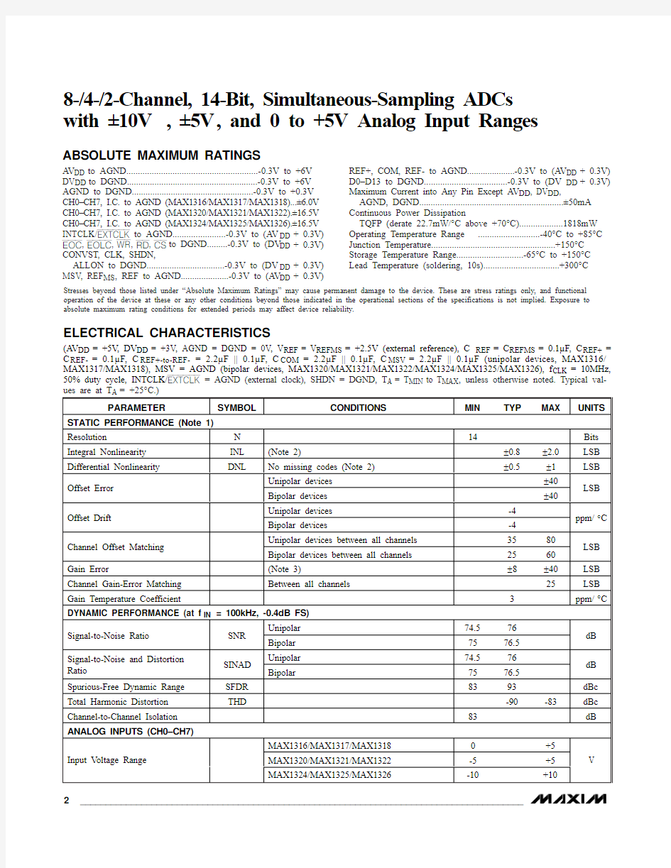
ABSOLUTE MAXIMUM RATINGS
ELECTRICAL CHARACTERISTICS
(AV DD = +5V, DV DD = +3V, AGND = DGND = 0V, V REF = V REFMS = +2.5V (external reference), C REF = C REFMS = 0.1μF, C REF+=C REF-= 0.1μF, C REF+-to-REF-= 2.2μF || 0.1μF, C COM = 2.2μF || 0.1μF, C MSV = 2.2μF || 0.1μF (unipolar devices, MAX1316/MAX1317/MAX1318), MSV = AGND (bipolar devices, MAX1320/MAX1321/MAX1322/MAX1324/MAX1325/MAX1326), f CLK = 10MHz,Stresses beyond those listed under “Absolute Maximum Ratings” may cause permanent damage to the device. These are stress ratings only, and functional operation of the device at these or any other conditions beyond those indicated in the operational sections of the specifications is not implied. Exposure to absolute maximum rating conditions for extended periods may affect device reliability.
AV DD to AGND.........................................................-0.3V to +6V DV DD to DGND.........................................................-0.3V to +6V AGND to DGND.....................................................-0.3V to +0.3V CH0–CH7, I.C. to AGND (MAX1316/MAX1317/MAX1318)...±6.0V CH0–CH7, I.C. to AGND (MAX1320/MAX1321/MAX1322).±16.5V CH0–CH7, I.C. to AGND (MAX1324/MAX1325/MAX1326).±16.5V INTCLK/EXTCLK to AGND.......................-0.3V to (AV DD + 0.3V)EOC , EOLC , WR , RD , CS to DGND.........-0.3V to (DV DD + 0.3V)CONVST, CLK, SHDN,
ALLON to DGND..................................-0.3V to (DV DD + 0.3V)MSV, REF MS , REF to AGND.....................-0.3V to (AV DD + 0.3V)
REF+, COM, REF- to AGND.....................-0.3V to (AV DD + 0.3V)D0–D13 to DGND....................................-0.3V to (DV DD + 0.3V)Maximum Current into Any Pin Except AV DD , DV DD ,
AGND, DGND...............................................................±50mA Continuous Power Dissipation
TQFP (derate 22.7mW/°C above +70°C)...................1818mW Operating Temperature Range ...........................-40°C to +85°C Junction Temperature......................................................+150°C Storage Temperature Range.............................-65°C to +150°C Lead Temperature (soldering, 10s).................................+300°C
ELECTRICAL CHARACTERISTICS (continued) MAX1316–MAX1318/MAX1320–MAX1322/MAX1324–MAX1326with ±10V, ±5V, and 0 to +5V Analog Input Ranges (AV DD= +5V, DV DD= +3V, AGND = DGND = 0V, V REF= V REFMS= +2.5V (external reference), C REF= C REFMS= 0.1μF, C REF+= C REF-= 0.1μF, C REF+-to-REF-= 2.2μF || 0.1μF, C COM= 2.2μF || 0.1μF, C MSV= 2.2μF || 0.1μF (unipolar devices, MAX1316/ MAX1317/MAX1318), MSV = AGND (bipolar devices, MAX1320/MAX1321/MAX1322/MAX1324/MAX1325/MAX1326), f CLK = 10MHz, 50% duty cycle, INTCLK/EXTCLK= AGND (external clock), SHDN = DGND, T A = T MIN to T MAX, unless otherwise noted. Typical val-
ues are at T A= +25°C.)
M A X 1316–M A X 1318/M A X 1320–M A X 1322/M A X 1324–M A X 1326
with ±10V , ±5V , and 0 to +5V Analog Input Ranges 4_______________________________________________________________________________________
ELECTRICAL CHARACTERISTICS (continued)
(AV DD = +5V, DV DD = +3V, AGND = DGND = 0V, V REF = V REFMS = +2.5V (external reference), C REF = C REFMS = 0.1μF, C REF+=C REF-= 0.1μF, C REF+-to-REF-= 2.2μF || 0.1μF, C COM = 2.2μF || 0.1μF, C MSV = 2.2μF || 0.1μF (unipolar devices, MAX1316/MAX1317/MAX1318), MSV = AGND (bipolar devices, MAX1320/MAX1321/MAX1322/MAX1324/MAX1325/MAX1326), f CLK = 10MHz,50% duty cycle, INTCLK/EXTCLK = AGND (external clock), SHDN = DGND, T A = T MIN to T MAX , unless otherwise noted. Typical val-ues are at T A = +25°C.)
MAX1316–MAX1318/MAX1320–MAX1322/MAX1324–MAX1326
with ±10V , ±5V , and 0 to +5V Analog Input Ranges
_______________________________________________________________________________________5
MAX1324/MAX1325/MAX1326, V IN = -10V to +10V.
Note 2:All channel performance is guaranteed by correlation to a single channel test.Note 3:Offset nulled.
Note 4:The analog input resistance is terminated to an internal bias point. Calculate the analog input current using:
for V CH within the input voltage range.
Note 5:Throughput rate is given per channel. Throughput rate is a function of clock frequency (f CLK = 10MHz). See the Data Throughput section for more information.
Note 6:
All analog inputs are driven with an FS 100kHz sine wave.
I V V R CH CH BIAS
CH ___
=
?TIMING CHARACTERISTICS (Figures 3, 4, 5, 6 and 7) (Tables 1, 3)
INTEGRAL NONLINEARITY vs. DIGITAL OUTPUT CODE
M A X 1316 t o c 01
DIGITAL OUTPUT CODE I N L (L S B )
12288
8192
4096
-0.75-0.50-0.2500.250.500.751.00-1.00
16384
DIFFERENTIAL NONLINEARITY vs. DIGITAL OUTPUT CODE
M A X 1316 t o c 02
DIGITAL OUTPUT CODE D N L (L S B )
12288
8192
4096
-0.75-0.50-0.2500.250.500.751.00-1.00
16384
ANALOG SUPPLY CURRENT vs. SUPPLY VOLTAGE
SUPPLY VOLTAGE (V)
S U P P L Y C U R R E N T (m A )
5.12
5.00
4.87
35
40
45
50
30
4.75
5.25
ANALOG SUPPLY CURRENT
vs. TEMPERATURE
TEMPERATURE (°C)
S U P P L Y C U R R E N T (m A )
60
35
10
-15
354045
5030-40
85
SHUTDOWN CURRENT vs. SUPPLY VOLTAGE
SUPPLY VOLTAGE (V)
S H U T D O W N C U R R E N T (μA )
4.5
3.5
0.20.4
0.6
0.802.5
5.5
SHUTDOWN CURRENT vs. TEMPERATURE
TEMPERATURE (°C)
S H U T D O W N C U R R E N T (μA )
60
35
10
-15
0.2
0.4
0.6
0.8
0-40
85
M A X 1316–M A X 1318/M A X 1320–M A X 1322/M A X 1324–M A X 1326
with ±10V , ±5V , and 0 to +5V Analog Input Ranges 6_______________________________________________________________________________________
TIMING CHARACTERISTICS (Figures 3, 4, 5, 6 and 7) (Tables 1, 3) (continued)
Note 7:
Shutdown current is measured with analog input floating. The large amplitude of the maximum shutdown current specifi-cation is due to automatic test equipment limitations.
Note 8:Defined as the change in positive full scale caused by ±5% variation in the nominal supply voltage.
Note 9:CONVST must remain low for at least the acquisition period. The maximum acquisition time is limited by internal capacitor
droop.
Note 10:CS -to-WR and CS -to-RD pins are internally AND together. Setup and hold times do not apply.
Note 11:Minimum clock frequency is limited only by the internal T/H droop rate. Limit the time between the falling edge of CONVST
to the falling edge of EOLC to a maximum of 0.25ms.
Note 12:To avoid T/H droop degrading the sampled analog input signals, the first clock pulse should occur within 10μs of the ris-ing edge of CONVST, and have a minimum clock frequency of 100kHz.
Typical Operating Characteristics
(AV DD = +5V, DV DD = +3V, AGND = DGND = 0V, V REF = V REFMS = +2.5V (external reference), see the Typical Operating Circuits sec-tion, f CLK = 10MHz, 50% duty cycle, INTCLK/EXTCLK = AGND (external clock), SHDN = DGND, T A = +25°C, unless otherwise noted.)
Typical Operating Characteristics (continued)
(AV DD = +5V, DV DD = +3V, AGND = DGND = 0V, V REF = V REFMS = +2.5V (external reference), see the Typical Operating Circuits sec-tion, f CLK = 10MHz, 50% duty cycle, INTCLK/EXTCLK = AGND (external clock), SHDN = DGND, T A = +25°C, unless otherwise noted.)
INTERNAL REFERENCE VOLTAGE vs. ANALOG SUPPLY VOLTAGE
AV DD (V)
V R E F (V )
5.2
5.1
4.8
4.9
5.02.49972.49982.49992.50002.50012.50022.50032.50042.4996
4.7
5.3
INTERNAL REFERENCE VOLTAGE
vs. TEMPERATURE
TEMPERATURE (°C)
V R E F (V )6035-15102.4972.4982.4992.5002.5012.5022.5032.5042.496
-40
85OFFSET ERROR vs. SUPPLY VOLTAGE
AV DD (V)
O F F S E T E R R O R (L S B )
5.15
5.05
4.95
4.85
-1.5-1.0-0.500.51.01.5-2.0
4.75
5.25
MAX1316–MAX1318/MAX1320–MAX1322/MAX1324–MAX1326
with ±10V , ±5V , and 0 to +5V Analog Input Ranges
_______________________________________________________________________________________7
OFFSET ERROR vs. TEMPERATURE
TEMPERATURE (°C)O F F S E T E R R O R (%F S R )
60
35
-15
10
-0.03-0.02
-0.0100.020.010.030.04-0.04
-40
85GAIN ERROR vs. SUPPLY VOLTAGE
M A X 1316 t o c 11
AV DD (V)G A I N E R R O R (L S B )
5.155.054.954.85101112131415169
4.75
5.25GAIN ERROR vs. TEMPERATURE
TEMPERATURE (°C)
G A I N E R R O R (%F S R )
6035-15100.020.030.040.050.070.060.080.09
0.01
-4085
Typical Operating Characteristics (continued)
(AV DD = +5V, DV DD = +3V, AGND = DGND = 0V, V REF = V REFMS = +2.5V (external reference), see the Typical Operating Circuits sec-tion, f CLK = 10MHz, 50% duty cycle, INTCLK/EXTCLK = AGND (external clock), SHDN = DGND, T A = +25°C, unless otherwise noted.)
FFT
FREQUENCY (MHz)
A M P L I T U D E (d
B )
0.20
0.15
0.10
0.05
-120-100-80-60-40-200-140
0.25
f ANALOG_IN = 103kHz f SAMPLE = 490kHz f CLK = 10MHz SINAD = 76.7dB SNR = 77.0dB THD = -88.3dB SFDR = 91.0dB
SIGNAL-TO-NOISE RATIO vs. CLOCK FREQUENCY
f CLK (MHz)
S N R (d B )
18
16
1412
10
71727374757677
787980708
20
SIGNAL-TO-NOISE PLUS DISTORTION
vs. CLOCK FREQUENCY
f CLK (MHz)
S I N A D (d B )
181614121071727374757677787980
70
820
EFFECTIVE NUMBER OF BITS vs. CLOCK FREQUENCY
f CLK (MHz)
E N O B (B I T S )
18
16
1412
10
8
20
11.011.512.012.5
13.013.5
10.5
TOTAL HARMONIC DISTORTION
vs. CLOCK FREQUENCY
M A X 1316 t o c 17
f CLK (MHz)
T H D (d B )
18
16
1412
10
8
20
-95-90-85-80-75-70-100
SPURIOUS-FREE DYNAMIC RANGE
vs. CLOCK FREQUENCY
M A X 1316 t o c 17b
f CLK (MHz)
S F D R (d B )
18
16
1412
10
8
20
6570
75808590
95100
60
M A X 1316–M A X 1318/M A X 1320–M A X 1322/M A X 1324–M A X 1326
with ±10V , ±5V , and 0 to +5V Analog Input Ranges 8_______________________________________________________________________________________
OUTPUT HISTOGRAM
(DC INPUT)
DIGITAL OUTPUT CODE
C O U N T S 8217
821682148215821182128213821050010001500200025003000350040004500
8209CONVERSION TIME vs. TEMPERATURE
TEMPERATURE (°C)
C O N V E R S I O N T I M E (μs )
603510-150.20.40.60.81.01.21.41.61.82.00
-40
85CONVERSION TIME
vs. ANALOG SUPPLY VOLTAGE
ANALOG SUPPLY VOLTAGE (V)C O N V E R S I O N T I M E (μs )
5.1255.0004.8750.20.40.60.81.01.21.41.61.82.004.750
5.250Typical Operating Characteristics (continued)
(AV DD = +5V, DV DD = +3V, AGND = DGND = 0V, V REF = V REFMS = +2.5V (external reference), see the Typical Operating Circuits sec-tion, f CLK = 10MHz, 50% duty cycle, INTCLK/EXTCLK = AGND (external clock), SHDN = DGND, T A = +25°C, unless otherwise noted.)
MAX1316–MAX1318/MAX1320–MAX1322/MAX1324–MAX1326
with ±10V , ±5V , and 0 to +5V Analog Input Ranges
_______________________________________________________________________________________9
Pin Description
M A X 1316–M A X 1318/M A X 1320–M A X 1322/M A X 1324–M A X 1326
with ±10V , ±5V , and 0 to +5V Analog Input Ranges 10______________________________________________________________________________________
MAX1316–MAX1318/MAX1320–MAX1322/MAX1324–MAX1326with ±10V, ±5V, and 0 to +5V Analog Input Ranges Array
______________________________________________________________________________________11
M A X 1316–M A X 1318/M A X 1320–M A X 1322/M A X 1324–M A X 1326
with ±10V , ±5V , and 0 to +5V Analog Input Ranges 12______________________________________________________________________________________
MAX1316–MAX1318/MAX1320–MAX1322/MAX1324–MAX1326
with ±10V , ±5V , and 0 to +5V Analog Input Ranges
______________________________________________________________________________________13
Detailed Description
The MAX1316–MAX1318/MAX1320–MAX1322/MAX1324-MAX1326 are 14-bit ADCs. They offer two, four, or eight (independently selectable) input channels, each with its own T/H circuitry. Simultaneous sampling of all active channels preserves relative phase information, making these devices ideal for motor control and power monitor-ing. These devices are available with 0 to +5V, ±5V, and ±10V input ranges. The 0 to +5V devices feature ±6V fault-tolerant inputs. The ±5V and ±10V devices feature ±16.5V fault-tolerant inputs. Two channels convert in 2μs;
all eight channels convert in 3.8μs, with a maximum 8-channel throughput of 263ksps per channel. Internal or external reference and internal- or external-clock capabil-ity offer great flexibility and ease of use. A write-only con-figuration register can mask out unused channels, and a shutdown feature reduces power. A 16.6MHz, 14-bit, par-allel data bus outputs the conversion result. Figure 1shows the functional diagram of these devices.
Analog Inputs
T/H
To preserve phase information across these multichan-nel devices, each input channel has a dedicated T/H amplifier.
Use a low-input source impedance to minimize gain-error harmonic distortion. The time required for the T/H to acquire an input signal depends on the input source impedance. If the input signal’s source impedance is high, the acquisition time lengthens and more time must be allowed between conversions. The acquisition time (t 1) is the maximum time the device takes to acquire the signal. Use the following formula to calcu-late acquisition time:
t 1= 10 (R S + R IN ) x 6pF
where R IN = 2.2k ?, R S = the input signal’s source impedance, and t 1is never less than 180ns. A source impedance of less than 100?does not significantly affect the ADC’s performance.
Figure 1. Functional Diagram
M A X 1316–M A X 1318/M A X 1320–M A X 1322/M A X 1324–M A X 1326
with ±10V , ±5V , and 0 to +5V Analog Input Ranges 14
______________________________________________________________________________________
To improve the input-signal bandwidth under AC condi-tions, drive the input with a wideband buffer (>50MHz)that can drive the ADC’s input capacitance and settle quickly. For example, the MAX4265 can be used for +5V unipolar devices, or the MAX4350 can be used for ±5V bipolar inputs.
The T/H aperture delay is typically 13ns. The aperture-delay mismatch between T/Hs of 50ps allows the relative phase information of up to eight different inputs to be preserved. Figure 2 shows a simplified equivalent input circuit, illustrating the ADC’s sampling architecture.Input Bandwidth
The input tracking circuitry has a 12MHz small-signal bandwidth, making it is possible to digitize high-speed transient events and measure periodic signals with bandwidths exceeding the ADC’s sampling rate by using undersampling techniques. To avoid high-frequency signals being aliased into the frequency band of interest,anti-alias filtering is recommended.
Input Range and Protection
These devices provide ±10V, ±5V, or 0 to +5V analog input voltage ranges. Figure 2 shows the equivalent input circuit. Overvoltage protection circuitry at the analog input provides ±16.5V fault protection for the bipolar input devices and ±6.0V fault protection for the unipolar input devices. This fault-protection circuit limits the current going into or out of the device to less than 50mA, provid-ing an added layer of protection from momentary over-voltage or undervoltage conditions at the analog input.
Power-Saving Modes
Shutdown Mode
During shutdown, the analog and digital circuits in the device power down and the device draws less than 100μA from AV DD , and less than 100μA from DV DD .Select shutdown mode using the SHDN input. Set SHDN high to enter shutdown mode. After coming out of shut-down, allow a 1ms wake-up time before making the first conversion. When using an external clock, apply at least 20 clock cycles with CONVST high before making the first conversion. When using internal-clock mode, wait at least 2μs before making the first conversion.
ALLON
ALLON is useful when some of the analog input channels are selected (see the Configuration Register section).Drive ALLON high to power up all input channel circuits,regardless of whether they are selected as active by the configuration register. Drive ALLON low or connect to ground to power only the input channels selected as active by the configuration register, saving 2mA per channel (typ). The wake-up time for any channel turned on with the configuration register is 2μs (typ) when ALLON is low. The wake-up time with ALLON high is only 0.01μs. New configuration-register information does not become active until the next CONVST falling edge. Therefore, when using software to control power states (ALLON = 0), pulse CONVST low once before applying the actual CONVST signal (Figure 3). With an external clock, apply at least 15 clock cycles before the second CONVST. If using internal-clock mode, wait at least 1.5μs or until the first EOC before generating the second CONVST.
Figure 2. Typical Input Circuit
MAX1316–MAX1318/MAX1320–MAX1322/MAX1324–MAX1326
with ±10V , ±5V , and 0 to +5V Analog Input Ranges
______________________________________________________________________________________15
Clock Modes
These devices provide an internal clock of 10MHz (typ). Alternatively, an external clock can be used.Internal Clock
Internal-clock mode frees the microprocessor from the burden of running the ADC conversion clock. For internal-clock operation, connect INTCLK/EXTCLK to AV DD and connect CLK to DGND. Table 1 illustrates the total con-version time using internal-clock mode.
External Clock
For external-clock operation, connect INTCLK/EXTCLK to AGND and connect an external-clock source to CLK.Note that INTCLK/EXTCLK is referenced to the analog power supply, AV DD . The external-clock frequency can be up to 15MHz, with a duty cycle between 30% and 70%. Clock frequencies of 100kHz and lower can be Selecting an Input Buffer
Most applications require an input buffer to achieve 14-bit accuracy. Although slew-rate and bandwidth are important, the most critical specification is settling time.The sampling requires a relatively brief sampling inter-val of 150ns. At the beginning of the acquisition, the internal sampling capacitor array connects to CH_ (the amplifier output), causing some output disturbance.Ensure the amplifier is capable of settling to at least 14-bit accuracy during this interval. Use a low-noise, low-distortion, wideband amplifier (such as the MAX4350 or
MAX4265), which settles quickly and is stable with the ADC’s capacitive load (in parallel with any bypass capacitors on the analog inputs).
Applications Section
Digital Interface
The bidirectional, parallel, digital interface sets the 8-bit configuration register (see the Configuration Register section) and outputs the 14-bit conversion result. The interface includes the following control signals: chip select (CS ), read (RD ), write (WR ), end of conversion (EOC ), end of last conversion (EOLC ), convert start (CONVST), shutdown (SHDN), all on (ALLON), internal-clock select (INTCLK /EXTCLK ), and external-clock input (CLK). Figures 4, 5, 6, 7, Table 4, and the Timing Characteristics section show the operation of the inter-face. D0–D7 are bidirectional, and D8–D13 are output only. All bits are high impedance when RD = 1 or CS = 1.
Configuration Register
Enable channels as active by writing to the configuration register through I/O lines D0–D7 (Table 2). The bits in the configuration register map directly to the channels, with D0 controlling channel zero, and D7 controlling channel seven. Setting any bit high activates the corresponding input channel, while resetting any bit low deactivates the corresponding channel. Devices with fewer than eight channels contain some bits that have no function.
Figure 3. Software Channel Wake-Up Timing (ALLON = 0)
M A X 1316–M A X 1318/M A X 1320–M A X 1322/M A X 1324–M A X 1326
with ±10V , ±5V , and 0 to +5V Analog Input Ranges 16
______________________________________________________________________________________
To write to the configuration register, pull CS and WR low, load bits D0–D7 onto the parallel bus, and force WR high. The data are latched on the rising edge of WR
(Figure 4). It is possible to write to the configuration register at any point during the conversion sequence;however, it is not active until the next convert-start sig-nal. At power-up, write to the configuration register to select the active channels before beginning a conver-sion. Shutdown does not change the configuration reg-ister. See the Shutdown Mode and the ALLON sections for information about using the configuration register for power saving.
Starting a Conversion
To start a conversion using internal-clock mode, pull CONVST low for at least the acquisition time (t 1). The T/H acquires the signal while CONVST is low, and con-version begins on the rising edge of CONVST. An end-of-conversion signal (EOC ) pulses low when the first result becomes available, and for each subsequent result until the end of the conversion cycle. The end-of-last-conversion signal (EOLC ) goes low when the last conversion result is available (Figures 5, 6, and 7).To start a conversion using external-clock mode, pull CONVST low for at least the acquisition time (t 1). The T/H acquires the signal while CONVST is low, and conversion begins on the rising edge of CONVST. Apply an external clock to CLK. To avoid T/H droop degrading the sampled analog input signals, the first clock pulse should occur within 10μs from the rising edge of CONVST, and have a minimum clock frequency of 100kHz. The first conversion result is available for read on the rising edge of the 17th clock cycle, and subsequent conversions after every third clock cycle thereafter (Figures 5, 6, and 7).
In both internal- and external-clock modes, CONVST must be held high until the last conversion result is read. For best operation, the rising edge of CONVST must be a clean, high-speed, low-jitter digital signal.Table 3 shows the total throughput as a function of the clock frequency and the number of channels selected for conversion. The calculations use the nominal speed of the internal clock (10MHz) and a 200ns CONVST pulse width.
NA = Not applicable.
Figure 4. Write Timing
MAX1316–MAX1318/MAX1320–MAX1322/MAX1324–MAX1326
with ±10V , ±5V , and 0 to +5V Analog Input Ranges
Data Throughput
The data throughput (f TH ) of the MAX1316–MAX1318/MAX1320–MAX1322/MAX1324–MAX1326 is a function of the clock speed (f CLK ). In internal-clock mode, f CLK =10MHz. In external-clock mode, 100kHz ≤f CLK ≤12.5MHz. When reading during conversion (Figures 5and 6), calculate f TH as follows:
where N is the number of active channels and t QUIET includes acquistion time t ACQ . t QUIET is the period of bus inactivity before the rising edge of CONVST. Typically use t QUIET = t ACQ + 50ns, and prevent disturbance on the output bus from corrupting signal acquistion. See the Starting a Conversion section for more information.
Reading a Conversion Result
Reading During a Conversion
Figures 5 and 6 show the interface signals for initiating a read operation during a conversion cycle. These figures show two channels selected for conversion. If more chan-nels are selected, the results are available successively every third clock cycle. CS can be low at all times; it can be low during the RD cycles, or it can be the same as RD .After initiating a conversion by bringing CONVST high,wait for EOC to go low (about 1.6μs in internal-clock mode or 17 clock cycles in external-clock mode) before reading the first conversion result. Read the conversion result by bringing RD low, thus latching the data to the parallel digital-output bus. Bring RD high to release the digital bus. Wait for the next falling edge of EOC (about 300ns in internal-clock mode or three clock cycles in external-clock mode) before reading the next result.When the last result is available, EOLC goes low.
f t x N f TH QUIET CLK =
+
+?+1
16311
()
M A X 1316–M A X 1318/M A X 1320–M A X 1322/M A X 1324–M A X 1326
with ±10V , ±5V , and 0 to +5V Analog Input Ranges 18
______________________________________________________________________________________
MAX1316–MAX1318/MAX1320–MAX1322/MAX1324–MAX1326
with ±10V , ±5V , and 0 to +5V Analog Input Ranges
______________________________________________________________________________________19
Reading After Conversion
Figure 7 shows the interface signals for a read operation after a conversion with all eight channels enabled. At the falling edge of EOLC , on the 38th clock pulse after the ini-tiation of a conversion, driving CS and RD low places the first conversion result onto the parallel bus, which can be latched on the rising edge of RD . Successive low pulses of RD place the successive conversion results onto the bus. Pulse CONVST low to initiate a new conversion.
Power-Up Reset
At power-up, all channels are selected for conversion (see the Configuration Register section). After applying power, allow a 1.0ms wake-up time to elapse before ini-tiating the first conversion. Then, hold CONVST high for at least 2.0μs after the wake-up time is complete. If using an external clock, apply 20 clock pulses to CLK with CONVST high before initiating the first conversion.
Reference
Internal Reference
The internal-reference circuits provide for analog input voltages of 0 to +5V unipolar (MAX1316/MAX1317/MAX1318), ±5V bipolar (MAX1320/MAX1321/MAX1322),or ±10V bipolar (MAX1324/MAX1325/MAX1326). Install external capacitors for reference stability, as indicated in Table 4, and as shown in the Typical Operating Circuits .External Reference
Connect a +2.0V to +3.0V external reference at REF MS and/or REF. When connecting an external reference, the input impedance is typically 5k ?. The external reference must be able to drive 200μA of current and have a low output impedance. For more information about using external references see the Transfer Functions section.
Layout, Grounding, and Bypassing
For best performance use PC boards with ground planes. Board layout should ensure that digital and
analog signal lines are separated from each other. Do not run analog and digital lines parallel to one another (especially clock lines), or do not run digital lines underneath the ADC package. Figure 8 shows the rec-ommended system ground connections when not using a ground plane. A single-point analog ground (star ground point) should be established at AGND, sepa-rate from the logic ground. All other analog grounds and DGND should be connected to this ground.
M A X 1316–M A X 1318/M A X 1320–M A X 1322/M A X 1324–M A X 1326
with ±10V , ±5V , and 0 to +5V Analog Input Ranges 20
______________________________________________________________________________________
No other digital system ground should be connected to this single-point analog ground. The ground return to the power supply for this ground should be low imped-ance and as short as possible for noise-free operation.High-frequency noise in the V DD power supply may affect the high-speed comparator in the ADC. Bypass these supplies to the single-point analog ground with
0.1μF and 2.2μF bypass capacitors close to the device.If the +5V power supply is very noisy, a ferrite bead can be connected as a lowpass filter, as shown in Figure 8.
Transfer Functions
Bipolar ±10V Devices
Table 5 and Figure 9 show the two’s complement trans-fer function for the MAX1324/MAX1325/MAX1326 with a ±10V input range. The full-scale input range (FSR) is eight times the voltage at REF. The internal +2.500V ref-erence gives a +20V FSR, while an external +2V to +3V reference allows an FSR of +16V to +24V, respectively.Calculate the LSB size using the following equation:
This equals 1.2207mV with a +2.5V internal reference.
The input range is centered about V MSV . Normally,MSV = AGND, and the input is symmetrical about zero.For a custom midscale voltage, drive MSV with an external voltage source. Noise present on MSV directly couples into the ADC result. Use a precision, low-drift voltage reference with adequate bypassing to prevent MSV from degrading ADC performance. For maximum FSR, be careful not to violate the absolute maximum voltage ratings of the analog inputs when choosing V MSV .
Determine the input voltage as a function of V REF ,V MSV , and the output code in decimal using the follow-ing equation:
Bipolar ±5V Devices
Table 6 and Figure 10 show the two’s complement transfer function for the MAX1320/MAX1321/MAX1322with a ±5V input range. The FSR is four times the volt-age at REF. The internal +2.500V reference gives a +10V FSR, while an external +2V to +3V reference allows an FSR of +8V to +12V, respectively. Calculate the LSB size using the following equation:
This equals 0.6104mV when using the internal reference.
V LSB CODE V CH MSV
_ =×+10Figure 9. ±10V Bipolar Transfer Function