PI3HDMI412FT-AZHE中文资料
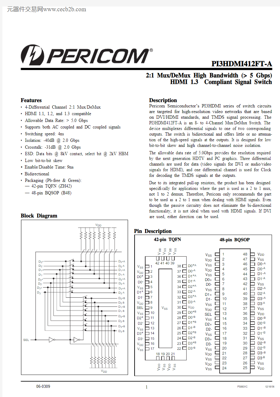
Block Diagram
PI3HDMI412FT-A 2:1 Mux/DeMux High Bandwidth (> 5 Gbps) HDMI 1.3 Compliant Signal Switch
Features
? 4-Differential Channel 2:1 Mux/DeMux
? HDMI 1.1, 1.2, and 1.3 compatible
? Allowable Data Rate: > 5.0 Gbps
? Supports both AC coupled and DC coupled signals ? Switching speed: 4ns
? Isolation: -40dB @ 2.0 Gbps
? Crosstalk: -31dB @ 2.0 Gbps
? ESD: Data bits @ 8kV contact, select bit @ 2kV HBM ? Low bit-to-bit skew
? Enable/Disable Time: 9ns
? Bidirectional
? Packaging (Pb-free & Green):
— 42-pin TQFN (ZH42)
— 48-pin BQSOP (B48)Description
Pericom Semiconductor’s PI3HDMI series of switch circuits are targeted for high-resolution video networks that are based on DVI/HDMI standards, and TMDS signal processing. The PI3HDMI412FT-A is an 8- to 4-Channel Mux/DeMux Switch. The device multiplexes differential signals to one of two corresponding outputs. The switch is bidirectional and offers little or no attenua-tion of the high-speed signals at the outputs. It is designed for low bit-to-bit skew and high channel-to-channel noise isolation.
The allowable data rate of 5.0Gbps provides the resolution required by the next generation HDTV and PC graphics. Three differential channels are used for data (video signals for DVI or audio/video signals for HDMI), and one differential channel is used for Clock for decoding the TMDS signals at the outputs.
Due to its integrated pull-up resistors, the product has been designed speci? cally for applications where the part is used as a 2 to 1 mux, not 1 to 2 demux. Therefore, Pericom only recommends the part to be used as a 2 to 1 mux when dealing with HDMI signals. Even though the passive circuitry does not eliminate the bi-directional functionality, it is not ideal when used with HDMI signals. If DVI are used, either direction can be used.
PI3HDMI412FT-A
2:1 Mux/DeMux High BW (> 5 Gbps)
HDMI 1.3 Compliant Signal Switch
Truth Table
SEL Function
L Dx → Dx A + Dx B pullups are active H
Dx → Dx B + Dx A pullups are active
Storage Temperature...........................................................–65°C to +150°C Supply V oltage to V SS Potential............................................–0.5V to +2.5V DC Input V oltage ..............................................................0V to V DD +0.5V DC Output Current.............................................................................120mA
Note: Stresses greater than those listed under MAX I M UM RAT I NGS may cause permanent damage to the de v ice. This is a stress rating only and func t ion a l op e r a t ion of the device at these or any other conditions above those indicated in the op-erational sections of this spec i ? c a t ion is not implied. Exposure to absolute max i m um rating con d i t ions for extended periods may affect re l i a bil i t y.
Maximum Ratings
(Above which useful life may be impaired. For user guide l ines, not tested.)
DC Electrical Characteristics for Switching over Operating Range (T A = –40°C to +85°C)
Paramenter Description Test Conditions (1)Min.Typ.(2)
Max.
Units
V IH (3)Input HIGH V oltage Guaranteed HIGH level 0.65(V DD -V SS )+V SS
V
V IL (3)Input LOW V oltage Guaranteed LOW level –0.5+V SS
0.35(V DD -V SS )+V SS
V IK Clamp Diode V oltage V DD =Max., I IN =–18mA
–0.7+V SS
–1.2+V SS
I IH Input HIGH Current V DD =Max., V IN =V DD ±5μA I IL
Input LOW Current
V DD =Max., V IN =V SS
±5
Notes:
1. For Max. or Min. conditions, use appropriate value speci ? ed under Electrical Characteristics for the applicable device type.
2. Typical values are at T A = 25°C ambient and maximum loading.
3. V IH & V IL are for SEL input only.
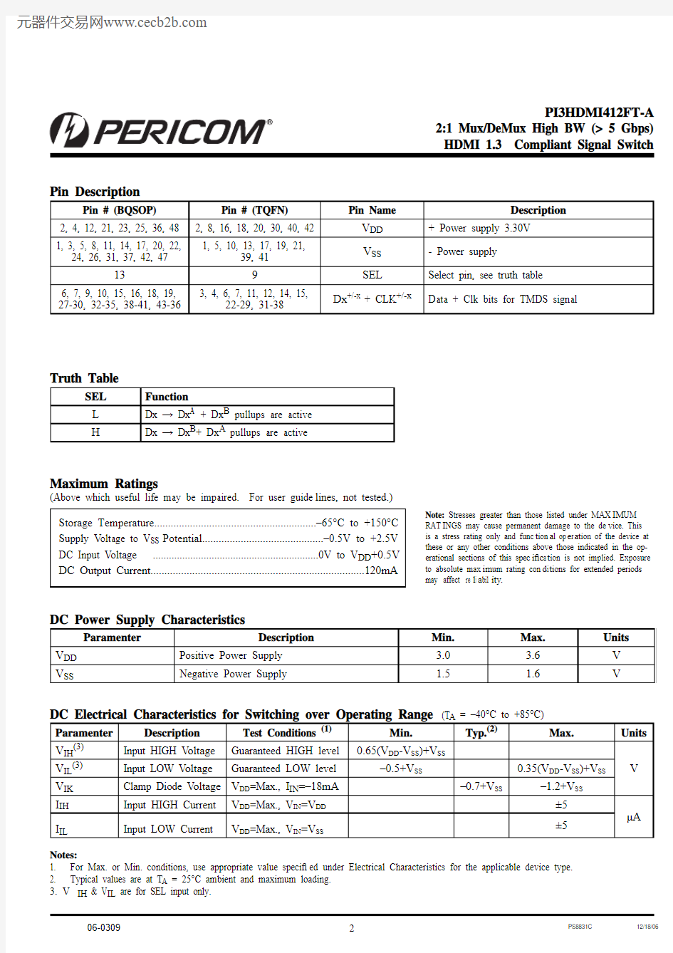
Pin Description
Pin # (BQSOP)Pin # (TQFN)Pin Name Description
2, 4, 12, 21, 23, 25, 36, 482, 8, 16, 18, 20, 30, 40, 42V DD + Power supply 3.30V 1, 3, 5, 8, 11, 14, 17, 20, 22, 24, 26, 31, 37, 42, 47
1, 5, 10, 13, 17, 19, 21,
39, 41
V SS - Power supply
13
9
SEL Select pin, see truth table 6, 7, 9, 10, 15, 16, 18, 19, 27-30, 32-35, 38-41, 43-36
3, 4, 6, 7, 11, 12, 14, 15,
22-29, 31-38
Dx +/-x + CLK +/-x
Data + Clk bits for TMDS signal
DC Power Supply Characteristics
Paramenter Description
Min.Max.Units V DD Positive Power Supply 3.0 3.6V V SS
Negative Power Supply
1.5
1.6
V
PI3HDMI412FT-A
2:1 Mux/DeMux High BW (> 5 Gbps)
HDMI 1.3 Compliant Signal Switch
Power Supply Characteristics
Parameters Description
Test Conditions (1)Min.
Typ.(2)Max.Units I CC
Quiescent Power Supply Current
V DD = Max., V IN = V DD or V SS
300
400
μA
Notes:
1. For Max. or Min. conditions, use appropriate value speci ? ed under Electrical Characteristics for the applicable device type.
2. Typical values are at T A = 25°C ambient and maximum loading.
Dynamic Electrical Characteristics Over the Operating Range (T A = -40o to +85oC)
Parameter Description Test Conditions
Min.
Typ.Max.
Units
X TALK Crosstalk See Fig. 1 for Measurement Setup,
@ 2.0 Gbps -31
dB
O IRR OFF Isolation See Fig. 2 for Measurement Setup,
@ 2.0 Gbps
-40BW
-3dB BW
2.7GHz
Insertion Loss
@ 1.65 Gbps
-0.87dB @ 2.0 Gbps -0.95@ 2.5 Gbps -1.18@ 3.3 Gbps -1.85
Notes:
1. For measurement setup, please see “Test Circuit For Electrical Characteristic” on page 8, and “Switching waveforms” on page 9
Switching Characteristics (T A = -40o to +85oC, V SS =0V , V DD =1.8V ±10%)
Paramenter Description
Min.Max.Units t PZH , t PZL Line Enable Time - SEL to N A , N B (1)0.58.0ns
t PHZ , t PLZ
Line Disable Time - SEL to N A , N B (1)
0.5
4.0
PI3HDMI412FT-A
2:1 Mux/DeMux High BW (> 5 Gbps)
HDMI 1.3 Compliant Signal Switch
Fig 2. Off-isolation setup
Fig 1. Crosstalk Setup
PI3HDMI412FT-A
2:1 Mux/DeMux High BW (> 5 Gbps)
HDMI 1.3 Compliant Signal Switch
Fig 3. Crosstalk
PI3HDMI412FT-A
2:1 Mux/DeMux High BW (> 5 Gbps)
HDMI 1.3 Compliant Signal Switch
Fig 4. Off Isolation
PI3HDMI412FT-A
2:1 Mux/DeMux High BW (> 5 Gbps)
HDMI 1.3 Compliant Signal Switch
Fig 5. Insertion Loss
PI3HDMI412FT-A
2:1 Mux/DeMux High BW (> 5 Gbps)
HDMI 1.3 Compliant Signal Switch
Fig 6. TMDS TP3 Rx eye compliance Test Setup
Application Measurements
PI3HDMI412FT-A Array
2:1 Mux/DeMux High BW (> 5 Gbps)
HDMI 1.3 Compliant Signal Switch
Fig 7. TP3 (Rx) with 2-meter cable eye measurements
(Right eye is with no switch. Left eye is with switch.)
Notes:
1. C L = Load capacitance: includes jig and probe capacitance.
2. R T = Termination resistance: should be equal to Z OUT of the Pulse Generator
3. Waveform 1 is for an output with internal conditions such that the output is low except when disabled by the output control.
Waveform 2 is for an output with internal conditions such that the output is high except when disabled by the output control.
4. All input impulses are supplied by generators having the following characteristics: PRR ≤ MHz, Z O = 50Ω, t R≤ 2.5ns, t F≤ 2.5ns.
5. The outputs are measured one at a time with one transition per measurement.
Switch Positions
Test Switch
t PLZ, t PZL 2 x (V DD - V SS)
t PHZ, t PZH V SS
Prop Delay Open
PI3HDMI412FT-A Array
2:1 Mux/DeMux High BW (> 5 Gbps)
HDMI 1.3 Compliant Signal Switch
Example of a circuit that also needs to be connected to the select lines of the PI3HDMI412FT-A
PI3HDMI412FT-A Array
2:1 Mux/DeMux High BW (> 5 Gbps)
HDMI 1.3 Compliant Signal Switch
PI3HDMI412FT-A Array
2:1 Mux/DeMux High BW (> 5 Gbps)
HDMI 1.3 Compliant Signal Switch
Ordering Information
Ordering Code Package Code Package Description
PI3HDMI412FT-AZHE ZH Pb-free & Green, 42-pin TQFN
PI3HDMI412FT-ABE B Pb-free & Green, 48-pin BQSOP
Notes:
? Thermal characteristics can be found on the company web site at https://www.360docs.net/doc/8d6711317.html,/packaging/
? E = Pb-free and Green
? Adding X suf? x = Tape/Reel
Pericom Semiconductor Corporation ? 1-800-435-2336 ? https://www.360docs.net/doc/8d6711317.html,