Wafer-Geo-Characteristics
Wafer Geometry Characteristics
Contents
1.1 Total Distance (TotDist) (1)
1.2 Thickness (LThk, CntThk) (1)
1.3 Average Thickness (AvgThk) (1)
1.4 Minimum-, Maximum Thickness (MinThk, MaxThk) and Total thickness variation (TTV) (2)
1.5 Standard Thickness (StdThk) (2)
1.6 Shape (3)
1.7 Max.Neg., Max. Pos. FPD, TIR (4)
1.8 Local Warp, Max. Neg. Warp, Max. Pos. Warp, Total Warp (5)
1.9 Bow-BF (5)
1.10 Bow-X, Bow-Y, Max-Bow-XY (5)
1.11 CntBow, Delta CntBow (6)
1.12 Sori (6)
1.13 Warp vs. Sori (7)
1.14 WBottom (8)
1.15 Geometry Measurement (9)
1.16 Resistivity Measurement in Silicon Wafers (11)
1.17 Measurement with Back Grinding Tape (13)
1.1 Total Distance (TotDist)
In our MX 203 Series Contactless Wafer Geometry Gauges, the evaluation of all wafer geometry characteristics is based upon distance measurements performed by multiple capacitive sensors embedded in two probe plates facing each other, and the surface of the test piece positioned in the air gap between the two plates. Thanks to correction data yielded by the calibration procedure, the two probe plates can be assumed to be perfectly flat, and to be mounted in a constant total distance between each other.
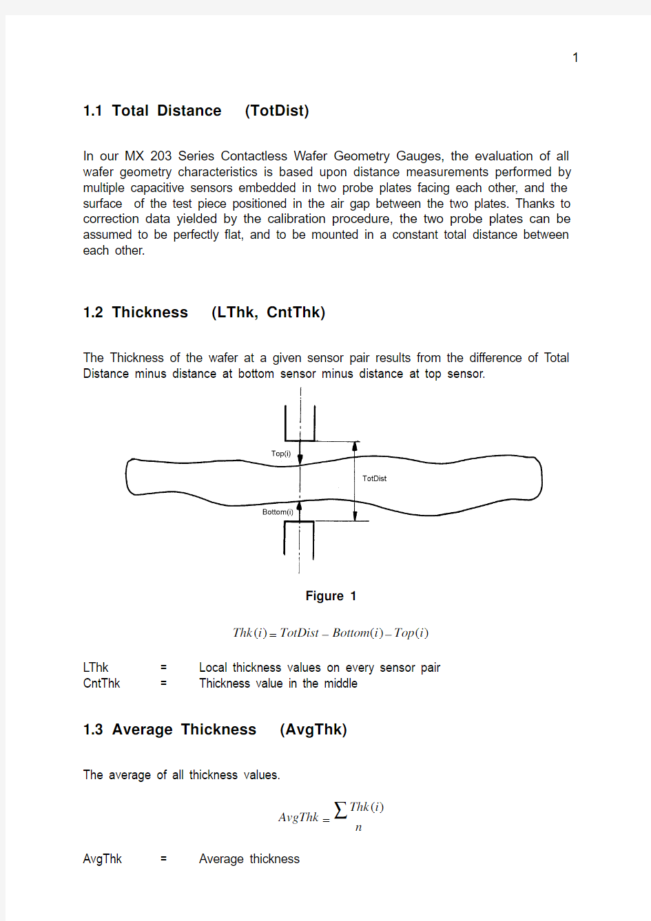
1.2 Thickness (LThk, CntThk)
The Thickness of the wafer at a given sensor pair results from the difference of Total Distance minus distance at bottom sensor minus distance at top sensor.
Figure 1
Thk i TotDist Bottom i Top i ()()()=??
LThk = Local thickness values on every sensor pair CntThk =
Thickness value in the middle
1.3 Average Thickness (AvgThk)
The average of all thickness values.
AvgThk Thk i n =∑()
AvgThk
=
Average thickness
1.4 Minimum-, Maximum Thickness (MinThk, MaxThk)
and Total thickness variation (TTV)
In an MX 203-8-37, e.g., a six inch wafer is measured at 21, a eight inch wafer at 37 sensor positions. The software computes the two thickness extrema, TTV (Total Thickness Variation) is the difference between them.
Figure 2
TTV MaxThk MinThk =?
MinThk = Minimum local thickness value MaxThk = Maximum local thickness value TTV =
Total thickness variation
1.5 Standard Thickness (StdThk)
x N x i i N
==∑11=>FS x x i i N
min ()=?=∑21
=>s FS N =
?min
1
=>
StdThk s N
=
N = number of local thickness values x = arithmetic mean value FS min = minimum mistake sum s = standard deviation StdThk
= standard deviation of arithmetic mean value
1.6 Shape
The mean value computed from the thickness values at the edge of wafer is subtracted from the center thickness value.
Figure 3
Shape CntThk Thk Shape i n Shape i n Shape =?
=∑(())
()
:()1
1.7 Max.Neg., Max. Pos. FPD, TIR
FPD = Focal plane deviation
TIR = total indicator reading
By representing all thickness values overhead a common plane, a vacuum chuck is simulated mathematically. By application of the …last squares fit“ algorithm to the given thickness values, a theoretical plane is computed, which is the best approximation to these values. It is called Focal Plane, at every sensor position, there is a local deviation between the plane and the local wafer thickness.
Figure 4
The extrema found in the given set of Focal Plane Deviation values are called Maxima Negative and Maximum Positive Focal Plane Deviation. TIR (Total Indicator Rating) is the sum of the absolute values of those two extrema.
1.8 Local Warp, Max. Neg. Warp, Max. Pos. Warp, Total Warp
Applying the least squares fit algorithm to center line values yields local deviations with respect to the approximated plane computed here. These are called Local Warp Values, their extrema are called Maximum Negative and Maximum Positive Warp, Total Warp is the sum of the absolute values of those two extrema.
Figure 5
1.9 Bow-BF
The Local Warp value in the center of the wafer is called Bow-BF
1.10 Bow-X, Bow-Y, Max-Bow-XY
Figure 6
Figure 7
Bow X C A B
?=?+
2
Bow Y C
D E
?=?
+
2
The biggest value is MaxBow-XY.
1.11 CntBow, Delta CntBow
Center Bow is a specific Bow who employs all edge warp values for calculation.
b
warp values at the border
number
warp value in the center c
=?
∑
Delta Center Bow is only available if you use the …Stress Modul“. It is the difference between a pre- and a post measurement.
?b b(post)-b(pre)
c c c
=
1.12 Sori
is the Japanese word for Warp. According to the JEIDA standard, it represents the maximum variations between individual points on the upper side of the wafer with respect to a least squares fit plane based on these points. E+H supplies special probe heads with multiple resting points for the wafer to approximate the required plane.
1.13 Warp vs. Sori
According SEMI’s Shape Decision Tree there is a very small difference only, depending on TTV. With low TTV values the difference is really negligible:
The original Japanese SORI definition (and also German DIN) has a serious difference:
The wafer is resting on a flat plane, not gravity corrected!
1.14 WBottom
In this case the warp is MUCH greater than the thickness and TTV. That is why it does not matter at all whether we use the lower surface of the wafer, or ist upper surface (sori) or the median (warp) to compute the wafer property “warp”.
WBOTTOM = local distance between sensor in the lower probe head and the bottom surface of the wafer.
MaxBtm = the maximum among the WBOTTOM values
1.15GEOMETRY MEASUREMENT
The top diagram on the attached sheet depicts all the world’s materials in a scale of their resistivities (? cm). For E+H geometry measurements, these materials are divided into two groups: conductors (on the left) and non-conductors (on the right). By using different capacitive principles, E+H gauges can accurately measure all wafer geometric characteristics – thickness, flatness, bow and warp. There is a small gap (gray area) between these two groups where measurements are difficult and sometimes impossible. E+H can slightly shift this gray area to the left or to the right by varying the carrier-frequency in their measuring systems.
GaAs has two widely separated resistivity ranges. On the low resistivity side is the conducting (doped) GaAs, which can be measured like Si. On the insulator side is a semi-insulating GaAs.
For Si and doped GaAs, the electric field lines from the sensor only travel down to the wafer surface. There is no influence of any material constants. Gauge calibration is accomplished using a standard metallic gauge block even for 100 ? cm wafer measurements. Bow and warp can easily be calculated.
For semi-insulating GaAs and other insulators, the electric field lines pass through the material and therefore, the permittivity “e” (relative dielectric constant) becomes a factor in the final results. Bow/warp measurements on these materials require special measuring heads (special sensor design).
It is possible to measure both conducting and insulated coated wafers as long as the film thickness is very small, or one of the two thickness (wafer or film) is exactly known. Otherwise, an indefinite equation exists.
10
1.16 RESISTIVITY MEASUREMENT IN SILICON WAFERS
To measure without contact the specific resistance of a conducting material requires the use of the well-known eddy current method. When a conducting material – such as silicon – is inserted into the air gap of an oscillating moving coil, this causes losses in the oscillation circuit to increase. This effect depends on the conductivity of the wafer and on the frequency of the oscillator. With regards to silicon, to achieve and
acceptable reproducibility on high impedance wafers, a high frequency oscillator is needed. However, this approach will not work with low impedance wafers because of skin effects. In this case, a lower frequency is needed.
The realization of a single measurement system for the five decimal powers from 1m ? cm to 100? cm would result in too many compromises; the exactness at the upper and lower end of the resistivity measuring range would not be sufficient. Therefore, E+H has designed into their resistivity measuring gauge a user selectable range:
High impedance wafers (0.1? cm -> 100? cm) -> 10MHz Oscillation Frequency Low impedance wafers (1m ? cm -> 1000m ? cm) -> 500kHz Oscillation Frequency
The measuring effect is proportional to the conductance of the measured target. That value is dependent on the wafer thickness – thicker wafers produce a higher output. The reciprocal value of this measured conductance is the resistance, commonly referred to as “Sheet Resistance” (R s in “Ohms per Square” (?/).
To come to the required material constant: “Resistivity”, the thickness of the target is needed and should be measured at the same point on the wafer: ρ = R s ? t
Example: a 1? cm wafer with 500μm thickness has a sheet resistance:
2005.01s =
?=cm cm R ?
The accuracy of the measurement is slightly lower in the high resistivity range, for
example the new gauge, the MX 608-8-R, has an accuracy of +0.5% for 0.001 - 20? cm wafers, and an accuracy of +1% for 20 - 80? cm wafers.
12
1.17 MEASUREMENTS WITH BACK GRINDING TAPE
MX 203 wafer thickness with back grinding tape is possible:
Σ?Σ+=r r ThF ThW R 1
R = displayed thickness result ThW = wafer thickness ThF = tape thickness
∑ r = permittivity (dielectric constant) of the tape material
For example a 10μm PP-tape on a 250μm wafer:
m R μ555.25525.2125.210250=
?+=
The tape thickness is partially added to the wafer thickness; this will depend on the type of material. If the tape thickness is known and if it has a low TTV value, the actual wafer thickness can be recalculated as well as its TTV.
13