FAR-F1DA-6M3120-G202中文资料
DS04-20100-3E
FUJITSU SEMICONDUCTOR
DATA SHEET
ASSP
TIMING EXTRACTION BANDPASS FILTER (1.5 to 100MHz)
F1/F2/F3 SERIES
s DESCRIPTION
The F1, F2 and F3 Series were developed as timing extraction filters for primary, secondary, and tertiary digital communication devices.
This new all-solid-state bandpass filter (BPF) uses a piezoelectric with a large electromechanical coefficient (lithium tantalate: LiT aO 3). The filter has a wide bandwidth, and is very stable.
s FEATURES
?Wide frequency range 1.5 to 100MHz ?Wide fractional bandwidth (%): 0.1 to 2.5?Low insertion loss: 6dB or less
?
Excellent temperature characteristics: 1.5 to 35MHz:±400ppm or less (0 to 60°C)
36 to 100MHz:–30ppm/°C (0 to 60°C)
?Small frequency deviation ?f O < ±500ppm eliminating the need for adjustment ?Highly reliable hermetically sealed package ?Compatible with small 14-pin DIP IC
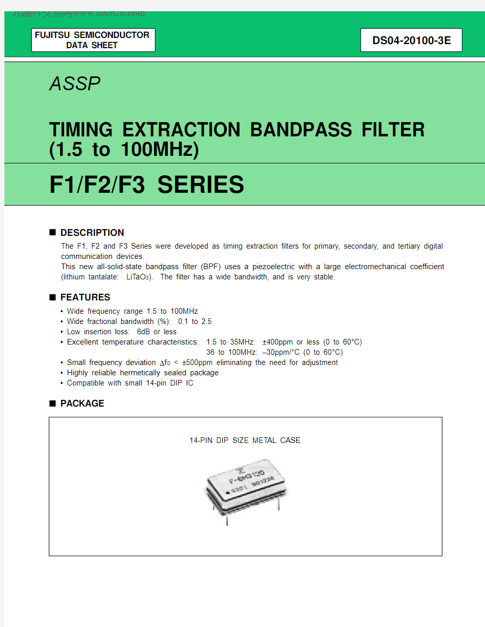
s PACKAGE
14-PIN DIP SIZE MET AL CASE
2
F1/F2/F3 SERIES
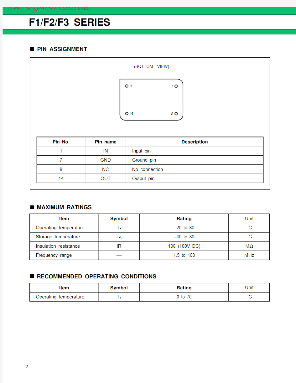
s PIN ASSIGNMENT
s MAXIMUM RATINGS
s RECOMMENDED OPERATING CONDITIONS
Item
Symbol Rating Unit Operating temperature T a –20 to 80°C Storage temperature T stg –40 to 80°C Insulation resistance IR 100 (100V DC)M ?Frequency range
––
1.5 to 100
MHz
Item
Symbol Rating Unit Operating temperature
T a
0 to 70
°C
F1/F2/F3 SERIES
s STANDARD FREQUENCY
Series Standard frequency Application Remarks
F1
1.544MHz For the U.S. and Japan (primary group)
2.048MHz For Europe (primary group)
3.088MHz For the U.S. and Japan (primary group) 1.544 × 2
3.152MHz For the U.S. and Japan (primary group)
4.096MHz For Europe (primary group) 2.048 × 2 6.312MHz For the U.S. and Japan (secondary group)
8.192MHz For the U.S. and Japan (secondary group)
8.448MHz For Europe (secondary group)
12.624MHz For the U.S. and Japan (secondary group) 6.312 × 2 16.384MHz For the U.S. and Japan (secondary group)8.192 × 2
F216.896MHz For Europe (secondary group)8.448 × 2 32.064MHz For Japan (tertiary group)
34.368MHz For Europe (tertiary group)
F344.736MHz For the U.S. (tertiary group)
3
F1/F2/F3 SERIES
s ELECTRICAL CHARACTERISTICS F1 Series
F2 Series F3 Series Item Symbol Condition
Rating
Unit Remarks
Min.Typical Max.
Frequency deviation?f O–––500––+500ppm f O standard Load Q Q––1000––40––
Insertion loss IL––––––6dB
Stop band attenuation A OUT f O ± 10MHz20––––dB
Frequency stability with temperature ?f (T a)–––400––+400ppm25°C standard,
T a = 0 to 70°C
Item Symbol Condition
Rating
Unit Remarks Min.Typical Max.
Frequency deviation?f O–––500––+500ppm f O standard Load Q Q––1000––40––
Insertion loss IL––––––6dB
Stop band attenuation A OUT f O ± 10MHz20––––dB
Frequency stability with temperature ?f (T a)–––400––+400ppm25°C standard,
T a = 0 to 70°C
Item Symbol Condition
Rating
Unit Remarks Min.Typical Max.
Frequency deviation?f O–––500––+500ppm f O standard Load Q Q––200––50––
Insertion loss IL––––––6dB
Stop band attenuation A OUT f O ± 10MHz20––––dB
Frequency stability with temperature ?f (T a)–––1350––750ppm25°C standard,
T a = 0 to 70°C
4
5
F1/F2/F3 SERIES
s ELECTRICAL CHARACTERISTICS
s TEST CIRCUIT
No.
Standard frequency (MHz)Part number
Specification
Load Q Insertion loss, IL (dB)Phase rotation θ (degree)Terminating impedance Z (?)
1 1.544
FAR-F1DA-1M5440-G201110 ±20 3 or less –90±207902 1.544FAR-F1DA-1M5440-G202110 ±20 3 or less –90±2010003 1.544FAR-F1DA-1M5440-G20360 ±10 3 or less –95±102035/20pF 4 1.544FAR-F1DA-1M5440-G205110 ±20 3 or less –90±2020005 2.048FAR-F1DA-2M0480-G20140 ±10 3 or less –90±1020356 2.048FAR-F1DA-2M0480-G202100 ±20 3 or less –90±2010007 3.088FAR-F1DA-3M0880-G201150 ±20 3 or less –90±206408 3.152FAR-F1DA-3M1520-G20185 ±15 3 or less –90±1512859 4.096FAR-F1DA-4M0960-G201110 ±20 3 or less –90±2075010 6.312FAR-F1DA-6M3120-G201110 ±20 3 or less –90±2098511 6.312FAR-F1DA-6M3120-G202110 ±20 3 or less –90±201000128.192FAR-F1DA-8M1920-G201100 ±20 3 or less –90±20980138.448FAR-F1DA-8M4480-G201110 ±20 3 or less –90±209801412.624FAR-F1DA-12M624-G201100 ±20 3 or less –90±205901516.384FAR-F1DA-16M384-G201100 ±20 3 or less –90±204101616.896FAR-F1DA-16M896-G201100 ±20 3 or less –90±203901732.064FAR-F2DA-32M064-G201100 ±10 3 or less –90±151001834.368FAR-F2DA-34M368-G201100 ±10 3 or less –90±1510019
44.736
FAR-F3DA-44M736-G201
65 ±15
6 or less
38±10
105
F1/F2/F3 SERIES
s CHARACTERISTICS SAMPLE
Pass band characteristic Stop band characteristic
T emperature characteristic
s PART NUMBERING SYSTEM
[Example]
FAR–F1DA––G
Series designation
Frequency designation:The standard frequency is designated in six alphanumeric characters. M is used
to designate the decimal point in MHz. Refer to “ELECTRIC CHARACTERISTICS”
in detail
Example: 1.544MHz: 1M5440
Serial number:The serial number is assigned from 201 to 999 (201 is normal).
6
F1/F2/F3 SERIES s MARKING
s DIMENSIONS
7
All Rights Reserved.
The contents of this document are subject to change without notice. Customers are advised to consult with FUJITSU sales representatives before ordering.
The information and circuit diagrams in this document presented as examples of semiconductor device applications, and are not intended to be incorporated in devices for actual use. Also, FUJITSU is unable to assume responsibility for infringement of any patent rights or other rights of third parties arising from the use of this information or circuit diagrams.
FUJITSU semiconductor devices are intended for use in standard applications (computers, office automation and other office equipment, industrial, communications, and measurement equipment, personal or household devices, etc.). CAUTION:
Customers considering the use of our products in special applications where failure or abnormal operation may directly affect human lives or cause physical injury or property damage, or where extremely high levels of reliability are demanded (such as aerospace systems, atomic energy controls, sea floor repeaters, vehicle operating controls, medical devices for life support, etc.) are requested to consult with FUJITSU sales representatives before such use. The company will not be responsible for damages arising from such use without prior approval.
Any semiconductor devices have inherently a certain rate of failure. You must protect against injury, damage or loss from such failures by incorporating safety design measures into your facility and equipment such as redundancy, fire protection, and prevention of over-current levels and other abnormal operating conditions.
If any products described in this document represent goods or technologies subject to certain restrictions on export under the Foreign Exchange and Foreign Trade Control Law of Japan, the prior authorization by Japanese government should be required for export of those products from Japan.