GR8876-Datasheet-V1.2

GR8876
Green-Mode PWM Controller with Integrated Protections
Features
High-voltage (500V) startup circuit Current mode PWM Very low startup current (<20uA) Under-voltage lockout (UVLO) Non-audible-noise green-mode control Programmable switching frequency Cycle-by-cycle peak current limiting Internal leading-edge blanking Internal slope compensation Internal 4ms soft start (Fs = 65KHz) VCC over-voltage clamp Gate output voltage clamp Soft driving for reducing EMI Over-voltage protection (OVP) on Vcc pin Over-load protection (OLP) Over-current protection (OCP) on CS pin 500mA driving capability
Applications
Open-frame SMPS Switching AC/DC adapter and battery charger
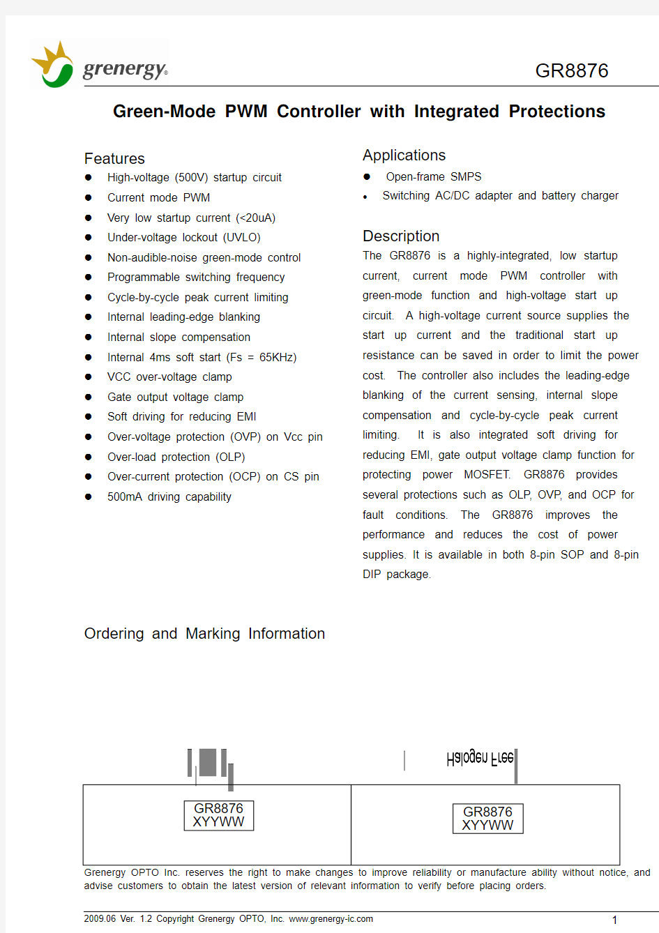
Ordering and Marking Information
DIP-8
SOP-8
GR8876 XYYWW XYYWW – Date Code
Grenergy OPTO Inc. reserves the right to make changes to improve reliability or manufacture ability without notice, and advise customers to obtain the latest version of relevant information to verify before placing orders.
2009.06 Ver. 1.2 Copyright Grenergy OPTO, Inc. https://www.360docs.net/doc/8412700922.html,
●
Description
The GR8876 is a highly-integrated, low startup current, current mode PWM controller with
green-mode function and high-voltage start up circuit. A high-voltage current source supplies the
start up current and the traditional start up resistance can be saved in order to limit the power cost. The controller also includes the leading-edge blanking of the current sensing, internal slope compensation and cycle-by-cycle peak current limiting. It is also integrated soft driving for
reducing EMI, gate output voltage clamp function for protecting power MOSFET. GR8876 provides
several protections such as OLP, OVP, and OCP for fault conditions. The GR8876 improves the
performance and reduces the cost of power supplies. It is available in both 8-pin SOP and 8-pin DIP package.
GR8876 XYYWW XYYWW – Date Code
1
GR8876
Pin Configuration
TOP VIEW
Pin Description
Pin 1 2 3 4 5 6 7 8 Symbol RT COMP CS GND OUT VCC NC HV Description Connecting a resistor to ground, this resistor determine the switching frequency Voltage feedback pin, by connecting a photo-coupler to control the duty cycle Current sense pin, connect to sense the MOSFET current Ground The output for driving the external MOSFET Power supply pin Unconnected pin This pin is connected to positive terminal of bulk capacitor. It provides the startup current. When UVLO (on) is tripped, this HV loop will be off thus limit the power loss on the startup circuit.
Absolute Maximum Ratings
Supply voltage VCC High-voltage pin, HV COMP, RT, CS -----------------------------------------------------------------------------------------------------------------------------------------------------------------------------------------------------35V - 0.3 ~ 500V -0.3 ~ 7V
---------------------------------------------------------------------------------------------------------
Storage temperature range
----------------------------------------------------------------------------------
- 65
DIP-8 package thermal resistance
-----------------------------------------------------------------------------) --------------------------------------------------------------------------------------------------
100 /W 400 mW 650mW
Power dissipation (DIP-8, at ambient temperature = 85 Lead temperature (SOP-8 & DIP-8, soldering, 10sec)
Lead temperature (All Pb free packages, soldering, 10sec) ESD voltage protection, human body model (except HV pin) ESD voltage protection, machine model
-----------------------------------------------------------------------------------------------
260
3KV 250V 2
----------------------------------------------------------------------------
2009.06 Ver. 1.2 Copyright Grenergy OPTO, Inc. https://www.360docs.net/doc/8412700922.html,
℃ ℃
℃ ℃
Power dissipation (SOP-8, at ambient temperature = 85
)
--------------------------------------------------------
230
℃ ℃
SOP-8 package thermal resistance
-------------------------------------------------------------------------------
℃ ℃
Operating ambient temperature
------------------------------------------------------------------------------
- 20
~ 85
~ 150
160 /W
℃ ℃ ℃
Junction temperature
-----------------------------------------------------------------------------------------------------
150
GR8876
Recommended Operating Conditions
Item Supply voltage VCC Switching frequency Min. 11 50 Max. 25 130 Unit V KHz
Block Diagram
2009.06 Ver. 1.2 Copyright Grenergy OPTO, Inc. https://www.360docs.net/doc/8412700922.html,
3
GR8876
Parameter HIGH-VOLTAGE SUPPLY (HV Pin) High-voltage current source (Vcc = 0V) Off-state leakage current SUPPLY VOLTAGE Startup current Operating current (with 1nF load on OUT pin), Vcomp = 0V Operating current (with 1nF load on OUT pin), Vcomp = 2.5V Operating current (with 1nF load on OUT pin), protection tripped (OLP, OVP) UVLO (on) UVLO (off) OVP level on VCC pin Vcc Zener clamp VOLTAGE FEEDBACK Short circuit current, Vcomp = 0V Open loop voltage, COMP pin open Green mode threshold voltage CURRENT SENSING Maximum input voltage, Vcs (off) Leading-edge blanking time Input impedance Delay to output OSCILLATOR 3 3 3 3 0.80 250 1 100 0.85 350 0.90 550 V nS 2 2 2 1 5 1.5 5.6 1.2 2 6 mA V V 6 6 6 6 6 6 6 6 1 1.5 0.1 13.5 8.0 26.5 2.3 2.5 0.5 14.5 9.0 27.5 35 20 3.3 4.0 1 15.8 10.0 30 uA mA mA mA V V V V 8 8 0.5 0 1.0 1.55 25 mA uA
nS
Green mode frequency (RT = 100K )
Voltage stability (Vcc = 11V ~ 25V) GATE DRIVER OUTPUT Output low level, VCC = 15V, Io = 20mA Output high level, VCC = 15V, Io = 20mA Rising time, load capacitance = 1000pF Falling time, load capacitance = 1000pF OLP OLP trip level, Vcomp (OLP) OLP delay time (note), Fs = 65KHz
2009.06 Ver. 1.2 Copyright Grenergy OPTO, Inc. https://www.360docs.net/doc/8412700922.html,
-(
Temp. stability
40° ~ 110° C C)
Ω
Ω
Frequency (RT = 100K
)
3 3 3 3
60 18
65 22
70 28 3 3
KHz KHz % %
1 1 1 1 8 150 50
1
V V nS nS
-
3.3
3.6 60
4
V mS
Ω
℃
Electrical Characteristics (TA = +25
unless otherwise stated, VCC = 15.0V) Pin Min. Typ. Max. Unit
M
4
021
08
℃/t 04
0
0451 71 91 f G / K H 12 z 32 52
℃ /t 02 1 08 04 0 0 47
8. 7 U V 6. 8 L O o f 4. 9 f / V 2. 01 11
℃/t
021
08
04
0
048.0 18.0 V c 28.0 s o f f 38.0 / V 48.0 58.0
2009.06 Ver. 1.2 Copyright Grenergy OPTO, Inc. https://www.360docs.net/doc/8412700922.html,
0 21
08
℃/ t 04
021
08
℃
/t 04
02 1
08
℃/ t 04
Typical Performance Characteristics
Fig.5
Fig.3
Fig.1
Fig.6
Fig.4
Fig.2
GR8876
5
0
0406 26 46 f O S C / K 66 H z 86 07
0
0431 8.31 U V 6.41L O o 4.51n / V 2.61 71
0
04 6. 0 8. 0 H 1 V C u r 2. 1 r e n t 4. 1 / m A 6. 1 8. 1
GR8876
Typical Performance Characteristics (Cont.)
Fig.7
Fig.8
Fig.9
Fig.10
Fig.11
Fig. 12
2009.06 Ver. 1.2 Copyright Grenergy OPTO, Inc. https://www.360docs.net/doc/8412700922.html,
021
021
08
08
℃ /t
℃/t 04
04
0
0
04-
0406
9.3
8.3
O L 7.3 P / V
6.3
5.3
58 56 M a 07x D u t 57y / ﹪ 08
021
08
℃
/t 04
0
044
6
5.4 V c o 5 m p o p 5.5 e n / V
5.6
6
GR8876
Application Information
Overview The GR8876 integrates several functions that are needed in the market. It includes green-mode controller and high-voltage start-up circuit which can save the power loss after startup. High-voltage Startup Circuit and Under-voltage Lockout (UVLO) GR8876 implements a high-voltage startup circuit, during the startup; high-voltage current sources are turned on and provide the start-up current as well as charge the Vcc capacitor. When the Vcc voltage is higher than the UVLO (on) threshold, the Oscillator The maximum duty-cycle of internal oscillator is limited to about 75% to avoid the transformer saturation. The frequency of the oscillator is decided by an external resistor connected from RT pin to ground. fosc = 6500(KHz)/R(Kohm). Where R is the resistor connected at RT pin. A
100Kohm resistor results in 65KHz switching frequency. The recommended range of oscillation
frequency is 50 KHz ~ 130 KHz. Green-mode Operation When the load decreases to an extent, the frequency of the controller will decrease so as to reduce the system power consumption. The minimum frequency is about 22 KHz which is outside the audio range. Leading-edge Blanking (LEB) Each time the power MOSFET is switched on, a turn-on spike will inevitably occur at the sensor resistor. To avoid fault trigger, a 250ns leadingedge blanking time is built in. Conventional RC
high-voltage current source will be turned off. Its leakage current is very low (8uA), which only consumes little power. By using such configuration, the traditional startup resistor is not needed and turn-on delay time will be almost the same no matter what the line voltage conditions are (Refer to Fig. 13).
filtering can therefore be omitted. During this blanking period, the current-limit comparator is disabled and cannot switch off the gate driver. Internal Slope Compensation A built-in slope compensation circuit is constructed in GR8876. When the switch is on, a ramp voltage is added to the sensed voltage across the CS pin, Fig. 13 which helps to stabilize the system and prevent sub-harmonic oscillations. A hysteresis UVLO comparator is implemented in GR8876, and then the turn-on and turn-off threshold levels are fixed at 14.5V and 9V respectively. This hysteresis shown in Fig.13 ensures that the start-up capacitor will be adequate to supply the chip during start-up.
2009.06 Ver. 1.2 Copyright Grenergy OPTO, Inc. https://www.360docs.net/doc/8412700922.html,
Gate Clamp/Soft Driving Driver is clamped by an internal 18V Zener diode. Those damages usually come from undesired over-voltage gate signals. Under the conditions
listed below, the gate output will turn off immediately to protect the power circuit. 7
GR8876
The GR8876 also has soft driving function to minimize EMI. Soft Start During initial power on, the GR8876 provides soft start function. It effectively suppresses the start up next UVLO (on). The VCC is working in hiccup mode. Fault Protections There are several critical protections integrated in the GR8876 to prevent the power supply or adapter from being damaged. Those damages usually come from open or short condition on the pins of GR8876. Under the conditions listed below, the gate output will turn off immediately to protect the power circuit:
peak current to reduce the power MOSFET drain voltage especially at high line. Over-load Protection (OLP) The controller has an over load protection function. An internal circuit detects the Comp pin level, when the level is larger than a threshold and the condition lasts more than 60ms, then the gate output will keep low level. The VCC will decrease to UVLO off level and the controller will be reset again. Fig.14 shows the waveform of the OLP operation.
. Gate pin short to ground . CS pin floating . RT pin floating . RT pin short to ground
Fig.14
Over-voltage Protection (OVP) on VCC To prevent power MOSFET from being damaged, the GR8876 is implemented an OVP function on VCC. When the VCC voltage is higher than the OVP threshold voltage, the output gate driver circuit will be shut down immediately to stop the switching of power MOSFET. The VCC OVP function is an auto-recovery type. If the OVP condition happens, the OUT pin will be disabled and will recover at the
2009.06 Ver. 1.2 Copyright Grenergy OPTO, Inc. https://www.360docs.net/doc/8412700922.html,
8
GR8876
Typical Application Circuit
2009.06 Ver. 1.2 Copyright Grenergy OPTO, Inc. https://www.360docs.net/doc/8412700922.html,
9
GR8876
Bom List
No. 1 2 3 4 5 6 7 8 9 10 11 12 13 14 15 16 17 18 19 20 21 22 23 24 25 26 27 28 29 30 31 32 BD1 C1 C2, C14, C20,C21 C3 C4 C5 C6, C11, C12,C19 C7 C8 C9 C10 C13 C15 C16, C17 C18 CN1 CR1 CR2 CR3 CR4, CR5 CR6 CR7 F1 HS1 HS2 J1, J2, J3 J4, J5 L1 L2 L3 NTC1 NTC2 Part Description Bridge, KBL406, DIP X-cap, 0.47uF, 275V, DIP N.A. Cap,102,1KV, DIP Cap,101,50V, SMD 0805 Y-CAP, CD222, 275V Cap,103,50V, SMD 0805 Cap,104,50V, SMD 0805 Cap,102, 200V, SMD 0805 Cap, 225, 50V, SMD 0805 Cap, 221, 50V, SMD 0805 1 1 1 4 1 1 1 1 , DIP 1 1 2 1 1 1 1 1 Quan. 1 1
E-Cap, 22uF, 50V, 105
E-Cap, 680uF, 25V, 105 , DIP, Low ESR E-Cap, 220uF, 25V, 105 ,DIP, Low ESR AC Input (3 Pin) FR107, DIP 1N4148, SMD FR104, DIP N.A. SBR10U100CT ISS181, SMD 3.15A, 250V, DIP Heat sink of Rectifier Heat sink of MOSFET 0R, SMD0805 0R, SMD1206 Common Chock, 700uH, DIP Common Chock,10mH, DIP 1.6uH, DIP N.A. N.A.
2009.06 Ver. 1.2 Copyright Grenergy OPTO, Inc. https://www.360docs.net/doc/8412700922.html,
℃ ℃ ℃ ℃
E-Cap,120uF, 400V, 105
, DIP
1 1 1 1 1 3 2 1 1 1
10
GR8876
Bom List (Cont.)
33 34 35 36 37 38 39 40 41 42 43 44 45 46 47 48 49 50 51 52 53 54 55 56 57 58 59 60 61 62 63 PCB Q1 Q2 Q3 R1A, R1B R2, R7, R8, R11, R14, R17, R32 R3A, R3B R4A, R4B, R5A, R5B R6, R33, R34 R9 R10 R12 R13 R15A, R15B R16 R18 R19 R20 R21 R22 R23 R24 R25, R26 R28 R29,R30 R31 T1 U1 U2 U3 ZD1 FR4, 102mm*39.0mm*1.0mm FPQF10N60,T0220 N.A. N.A. 1 1
N.A. N.A.
0R, SMD0805
100K, 1 33R, 5 22R, 5
0.0170R, 4.0mm
62K, 5
100R, 5 1.5K, 5 10R, 5
2.2K, 5
16.5K, 1 5K, 1
15K, 5
4.3K,1
1.5K, 1
P0T-3019, 550uH GR8876, SOP-8 PC817, DIP-4 TSM103, SOP-8 N.A.
2009.06 Ver. 1.2 Copyright Grenergy OPTO, Inc. https://www.360docs.net/doc/8412700922.html,
% % % % % % % % % % %
68K, 1
% % % %
2.2R, 5
, SMD1206 , SMD0805
, SMD0805 , SMD1206
, SMD0805 , SMD0805 , SMD0805
, SMD0805
, SMD0805 , SMD0805 , SMD0805
, SMD0805 , SMD0805 , SMD0805 , DIP
%
0.33R, 1W, 1
%
68K, 5
%
1M, 5
, SMD1206
2
, SMD1206
4 3
, Rcs
1 1 1 1 2 1 1 1 1 1 1 1 1 2 1 2 1 1 1 1 1
11
GR8876
Package Information
SOP-8
Symbols
A A1 A2 D E H L
o
Min.
0.053 0.004 0.053 0.189 0.150 0.228 0.016 0
Max.
0.069 0.010 0.059 0.196 0.157 0.244 0.050 8 UNIT: INCH
2009.06 Ver. 1.2 Copyright Grenergy OPTO, Inc. https://www.360docs.net/doc/8412700922.html,
θ
12
GR8876
Package Information
DIP-8
Symbols
A A1 A2 D E E1 L eB
o
MIN.
0.015 0.125 0.355
NOM.
0.130 0.365 0.300 BSC.
MAX.
0.210 0.135 0.400
0.245 0.115 0.335 0
0.250 0.130 0.355 7
0.255 0.150 0.375 15 UNIT: INCH
2009.06 Ver. 1.2 Copyright Grenergy OPTO, Inc. https://www.360docs.net/doc/8412700922.html,
θ
13
GR8876
Carrier Tape & Reel Dimensions
SOP- 8
Application
A 330.0 2.0
H 50 MIN. P1 8.0 0.10
±
T1
C
d 1.5 MIN. D1 1.5 MIN.
D
W
E1
F 5.5 0.05 K0
± ±
SOP-8
P0 4.0 0.10
±
P2 2.0 0.05
±
D0 1.5+0.10 -0.00
T 0.6+0.00 -0.40
A0
±
B0
±
6.40 0.20 5.20 0.20 2.10 0.20
Devices Per Unit
Application SOP- 8 Carrier Width 12 Cover Tape Width Devices Per Reel 2500
________________________________________________________________________
Grenergy OPTO, Inc. reserves the right to make corrections, modifications, enhancements, improvements, and other changes to its products and services at any time and to discontinue any product or service without notice. Customers should obtain the latest relevant information before placing orders and should verify that such information is current and complete.
2009.06 Ver. 1.2 Copyright Grenergy OPTO, Inc. https://www.360docs.net/doc/8412700922.html,
±
±
12.4+2.00 13.0+0.50 -0.00 -0.20
20.2 MIN. 12.0 0.30 1.75 0.10
±
(mm)
14