高适应性的混合直流换流器Hybrid DC Converter with Wide ZVS Range
Hybrid DC Converter with Wide ZVS Range Bor-Ren Lin, Senior Member, IEEE, and Kuan-Hao Chen
Department of Electrical Engineering
National Yunlin University of Science and Technology, Yunlin 640, Taiwan
Abstract–This paper presents a new soft switching dc-dc converter including a three-level pulse-width modulation (PMW) converter and a series resonant converter with same active switches to extend zero voltage switching (ZVS) range and to reduce circulating current losses on the primary side during freewheeling intervals. The phase-shift PWM scheme is adopted to generate the properly gating signals for active switches in three-level converter and regulate output voltage at the designed voltage level. Series resonant converter with fixed switching frequency is adopted to extend the ZVS range of active switches at lagging leg. The circulating current losses in three-level converter are reduced by parallel connection of output sides of three-level converter and series resonant converter. In order to reduce the circulating current losses in series resonant converter, the switching frequency is higher than the series resonant frequency. Thus, the circulating losses in three-level converter and series resonant converter are all improved. The circuit efficiency of the proposed converter is improved. Finally, experiments with a 1.44k W prototype circuit are provided to verify the effectiveness of the proposed converter.
Index Terms—Soft switching dc-dc converter, full-bridge converter, series resonant converter, zero voltage switching.
I.I NTRODUCTION
Medium or high power ac-dc converters with high power density and high efficiency have been proposed and used in industry switching mode power supplies and plug-in hybrid electric vehicle battery chargers [1]-[2]. In order to meet the power quality demands, single-phase or three-phase bridge/bridgeless power factor correctors (PFC) with boost voltage type have been proposed. Thus, a stable dc bus voltage with V dc=500V-800V is provided by a three-phase PFC. Three-level dc-dc converters [3]-[5] with low voltage stress of active switches are widely adopted in industry applications. Phase-shift pulse-width modulation (PWM) is normally used to generate the gate singles of three-level converters. However, active switches at lagging leg are more difficult to achieve zero voltage switching (ZVS) at light load due to the limited energy stored in primary leakage inductance. If the primary leakage inductance is increased [6] or external resonant inductance [1] is added on the primary side, the ZVS range can be improved but the duty cycle loss in freewheeling intervals is also increased that will decrease the effective duty cycle on the secondary side. The more secondary winding turns are needed and it will increase the copper losses of transformer, voltage rating of rectifier diodes and conduction losses of active switches. Auxiliary circuits added on the primary side have been proposed in [7]-[9] to extend the ZVS range. The switching power loss of active switches is reduced but the power losses of additional auxiliary circuits are increased. In [10]-[11], LLC converter and full-bridge converter share active switches at lagging leg to extend the ZVS range of lagging leg from light load to full load. The circulating current losses on the primary side during freewheeling intervals are the other main issue in conventional three-level converter. The high circulating current will increase circuit conduction losses on active switches and transformer windings and decrease circuit efficiency. The active and passive clamp circuits [2] and [12] are adopted at the secondary side to limit voltage overshoots and oscillations across the output diodes when they are turned off and to improve the circulating current losses on the primary side. This paper presents a hybrid three-level ZVS converter including a phase-shift PWM converter and a resonant converter with fixed switching frequency to achieve the functions of wide range of ZVS turn-on for lagging-switch, low circulating current losses and high circuit efficiency. Half-bridge LLC resonant converter shares the same active switches at lagging leg in the conventional three-level PWM converter. Since the LLC converter is operated at f sw (switching frequency) > f r (series resonant frequency), the active switches can be turned on under ZVS from zero to full load with low circulating current losses. The ZVS range of lagging-leg switches can be extended from zero to full load. The leakage inductance or external inductance in three-level converter can be reduced to decrease duty cycle losses and the circulating current during freewheeling intervals. The output sides of LLC converter and three-level PWM converter are connected in parallel with a clamp diode. When the primary voltage of three-level converter is positive or negative, the output power is delivered from input to output through three-level converter. However, the output power is transferred from input to output through LLC converter when three-level converter is operated at freewheeling interval. Thus, three-level converter and LLC converter transfer energy from input to output within the switching cycle to achieve more effective energy transfer. The circulating current of three-level converter during the freewheeling interval can be reduced due to the clamp diode. Finally, the effectiveness of the proposed converter is verified
k
W prototype circuit.
V
o
v
current
v S1v S2v S3v S4
(b)
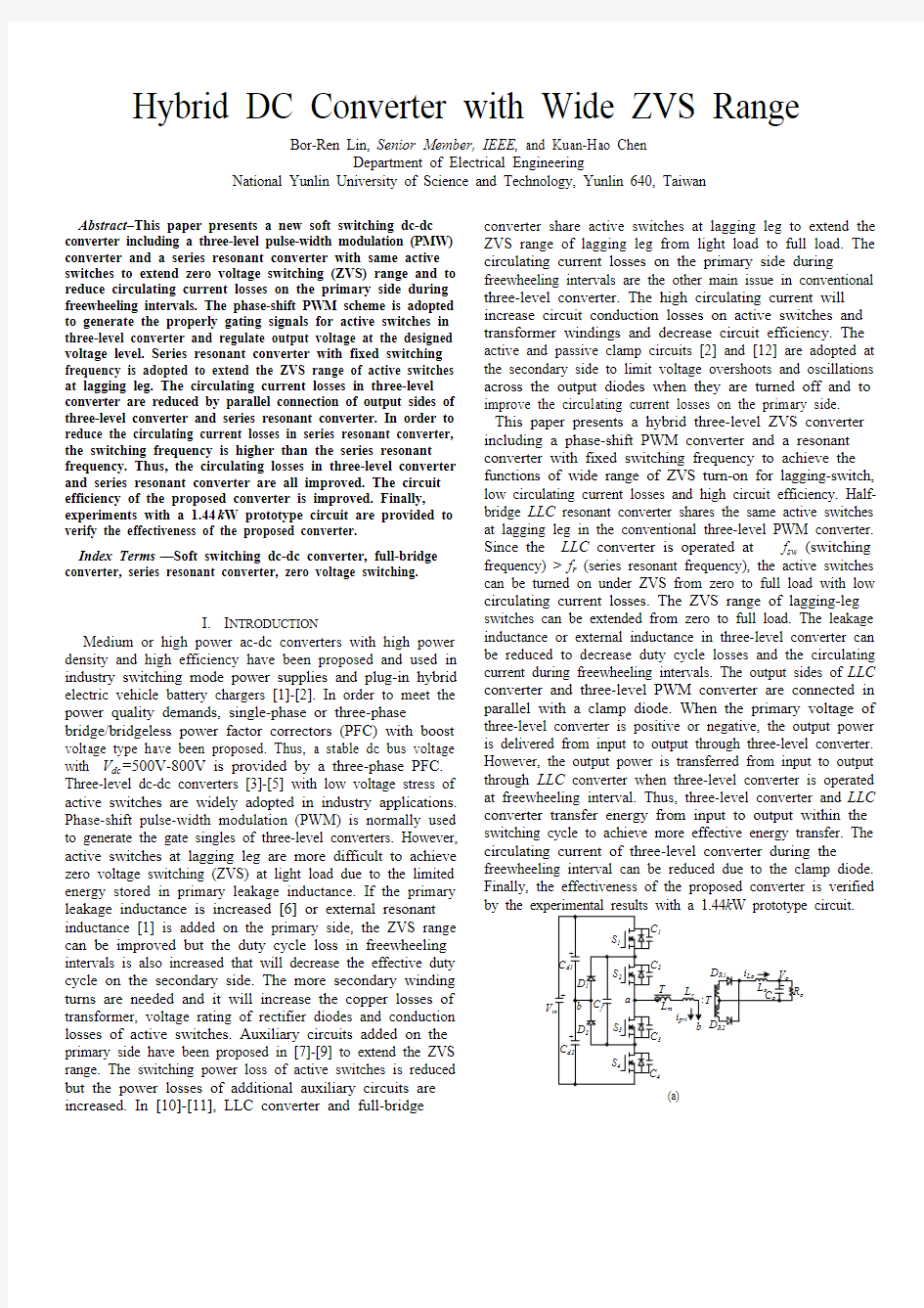
Fig. 1. Conventional three-level converter (a) circuit configuration (b) key waveforms.
(a)
(b)
Fig. 2. Conventional three-level converter with passive snubber (a) circuit configuration (b) key waveforms.
C
R2
o
(a)
(b)
(c)
Fig. 3. Conventional LLC converter (a) circuit configuration (b) operating at f s
II. C IRCUIT C ONFIGURATION AND O PERATION P RINCIPLES A. Circuit Configuration
Fig. 1 shows the circuit diagram of the conventional three-level ZVS converter with phase-shift PWM scheme. There is a serious circulating current during the freewheeling interval (v ab =0). No power is transferred from input to output at
freewheeling interval. Thus, the circulating current will increase the conduction losses on active switches and transformer windings and decrease the circuit efficiency especially at high input voltage and full load. Low cost passive
snubber as shown in Fig. 2 is normally adopted on the secondary side to limit the voltage overshoots and oscillations across the rectifier diodes and to reduce the circulating current. The clamp capacitor C a is operated as a constant dc voltage in
steady state. When three-level converter is operated at freewheeling interval, the clamp capacitor voltage V Ca can help to decrease the primary current and reduce the conduction losses on active switches. Fig. 3 shows the conventional half-bridge LLC converter with two different operation conditions (f sw
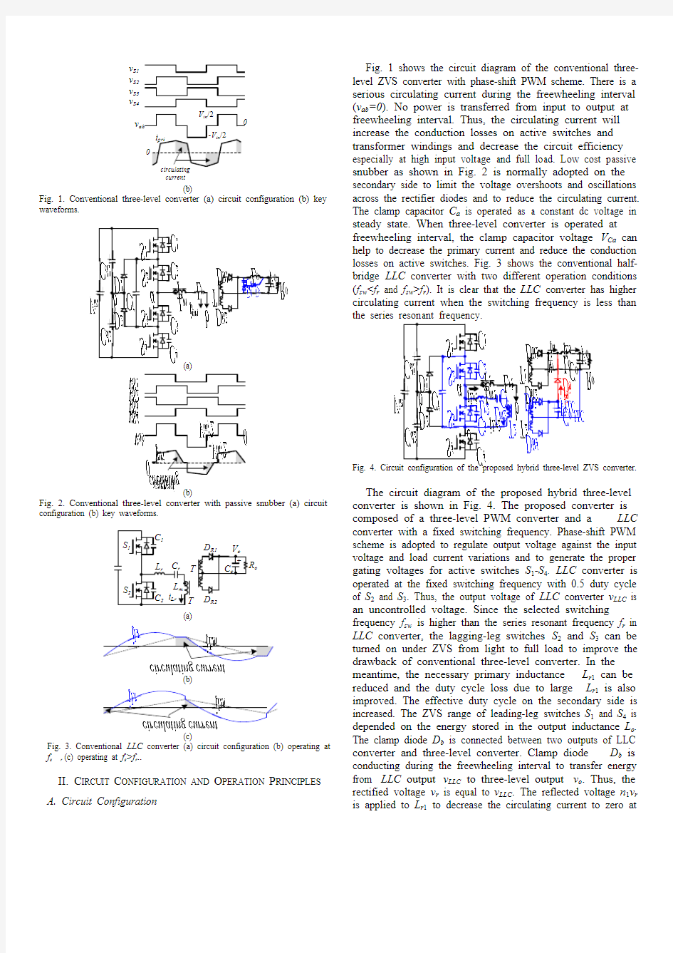
Fig. 4. Circuit configuration of the proposed hybrid three-level ZVS converter.
The circuit diagram of the proposed hybrid three-level converter is shown in Fig. 4. The proposed converter is composed of a three-level PWM converter and a LLC converter with a fixed switching frequency. Phase-shift PWM scheme is adopted to regulate output voltage against the input voltage and load current variations and to generate the proper gating voltages for active switches S 1-S 4. LLC converter is operated at the fixed switching frequency with 0.5 duty cycle of S 2 and S 3. Thus, the output voltage of LLC converter v LLC is an uncontrolled voltage. Since the selected switching frequency f sw is higher than the series resonant frequency f r in LLC converter, the lagging-leg switches S 2 and S 3 can be turned on under ZVS from light to full load to improve the drawback of conventional three-level converter. In the meantime, the necessary primary inductance L r 1 can be reduced and the duty cycle loss due to large L r 1 is also improved. The effective duty cycle on the secondary side is increased. The ZVS range of leading-leg switches S 1 and S 4 is depended on the energy stored in the output inductance L o . The clamp diode D b is connected between two outputs of LLC converter and three-level converter. Clamp diode D b is conducting during the freewheeling interval to transfer energy from LLC output v LLC to three-level output v o . Thus, the rectified voltage v r is equal to v LLC . The reflected voltage n 1v r is applied to L r 1 to decrease the circulating current to zero at
the freewheeling interval. In the meantime, the voltage across output inductor is equal to v LLC -v o instead of -v o so that the output inductance in the proposed hybrid converter can be reduced.
S 1S 2S 3S 4v
v i i i i i in /2
Fig. 5. Key waveforms of the proposed converter during half switching cycle.
B. Operation Principles
The duty cycle of active switches S 1-S 4 is equal to 0.5. MOSFETs S 1-S 4 and rectifier diodes D R 1-D R 4, D 1-D 2 and D b are assumed ideal. Voltages across C d 1, C d 2, C f , C o,LLC and C o are assumed constant. Turns ratios of T 1 and T 2 are n 1=n p 1/n s 1=n p 1/n s 2 and n 2=n p 2/n s 3=n p 2/n s 4, respectively. C 1=C 2=C 3=C 4=C oss and V Cd1=V Cd2=V Cf =V in /2. Fig. 5 shows the theoretical key waveforms of the proposed hybrid converter in a switching period. Based on the on/off states of S 1-S 4, D R 1-D R 4, D 1-D 2 and D b , there are six topological stages during each half switching period. The equivalent operation circuits for different topological stages are shown in Fig. 6. Prior to t 0, MOSFETs S 1 and S 2 and the rectifier diodes D R 1 and D R 3 are conducting. Inductor currents i Lr1 and i Lr2 are all positive.
Stage 1 [t 0 - t 1]: Switch S 1 is turned off at time t 0. i Lr1 and i Lr2 start to charge C 1 and discharge C 4 via capacitor C f . The ZVS condition of S 4 is given as:
2
)()()(20
2
22021211in
oss Lr r Lr o r V C t i L t i L n L ≥++ (1)
The energy stored in L o is reflected to the primary side to discharge C 4. Thus, the ZVS condition of S 4 is easily achieved. This stage ends at t 1 when v C 1=V in /2 and v C 4=0. The time interval of stage 1 is given as:
max
,21max ,02010101/)()(Lr Lo in
oss Lr Lr in oss i n i V C t i t i V C t t t +≈+=?=Δ (2)
To ensure the ZVS operation of S 4, the dead time between S 1 and S 4 should be greater than Δt 01.
Stage 2 [t 1 - t 2]: This stage starts at t 1 when v C 1=V in /2, v C 4=0, and D 1 is conducting. The ac terminal voltages v ab =0 and v ac =v Cf =V in /2. Thus, the clamp diode D b is conducting and the inductor voltage v Lo =V LLC -V o <0. The inductor current i Lo decreases with the slope of (V LLC -V o )/L o in this stage. The reflected secondary windings voltage -n 1V LLC is applied to L r 1 so that i Lr 1 decreases with the slope of -n 1V LLC /L r 1. In
conventional three-level converter, the primary current i Lr 1 is still keeping at high current value so that the circulating current losses are serious in the freewheeling interval. In the proposed converter, the primary side current of three-level converter can be decreased to zero very quickly due to apply a negative voltage -n 1V LLC to inductor L r 1. Thus, the circulating current can be rapidly reduced at the beginning of the freewheeling interval. In this stage, the energy stored in C o,LLC is transferred to output load through D b and L o , i a decreases, and i b increases. At the same time, LLC converter is in the
o,LLC
.
Fig. 6. Operation stages of the proposed converter in a half switching cycle (a) stage 1 (b) stage 2 (c) stage 3 (d) stage 4 (e) stage 5 (f) stage 6.
Stage 3 [t 2 - t 3]: This stage starts at t 2 when the primary and secondary side currents i Lr 1 and i a of three-level converter are decreased to zero. The primary and secondary sides of transformer T 1 is disconnected and the LLC circuit continuous to transfer energy from input source to output load with i Lo =i b . Stage 4 [t 3 - t 4]: This stage start at t 3 when S 2 is turned off. i Lr 1 and i Lr 2 start to charge C 2 and discharge C 3. The ZVS condition of S 3 is given as:
2
)(2
3222in
oss Lr r V C t i L ≥
(3)
Since the LLC converter is operated at the inductive load (f sw >f r ), the inductor current i Lr 2 is lagging to the input fundamental voltage v ac,f . Thus, S 3 can be turned on under ZVS at t 4 from light load to full load.
Stage 5 [t 4 - t 5]: This stage starts at t 4 when capacitor voltage v C 3 is decreased to zero. Since i Lr 1(t 4)+i Lr 2(t 4)>0, the anti-parallel diode of S 3 is conducting. Switch S 3 can be turned on at this moment to achieve ZVS. The ac terminal voltages v ab =-V in /2 and v ac =0, and the clamp diode D b is still conductin g to transfer energy from C o,LLC to output load. The rectified voltage v r =V LLC and the output inductor voltage v Lo=V LLC -V o <0. Thus, i Lo decreases with the slope of (V LLC -V o )/L o . The primary side inductor voltage v Lr1=n 1V LLC -V in /2<0. LLC converter is in the resonant mode with v ac =0. Thus, i Lr 2 decreases in this stage. The clamp diode current is also decreased i Db =i Lo +n 1i Lr 1. Both three-level converter and LLC converter transfer energy from input source voltage to output load in this stage. The inductor current i Lr 1 decreases linearly until it equals -i Lo /n 1. Then D b is off. The time interval in this stage is given as:
LLC
in Lo r V n V n t i L t t t 11
5145452//)(?≈?=Δ (4)
Stage 6 [t 5 - t 6]: This stage starts at t 5 when i a =i Lo and i b =0. Then the clamp diode D b is off. The energy is transferred from input voltage to output load through three-level converter and LLC circuit transfers energy to C o,LLC . The output inductor voltage v Lo =V in /(2n 1)-V o >0 and i Lo increases in this stage. This stage ends at t 6 when S 4 is turned off. Then, the circuit operations of the proposed converter in a half switching cycle are completed.
III. C IRCUIT C HARACTERISTICS OF THE P ROPOSED
C ONVERTER The energy of the proposed converter is transferred from input side to output side by both LLC circuit and three-level circuit. In stages 2-5, LLC circuit transfers energy from input voltage to output load. On the other hand, three-level circuit transfers energy from input side to output load in stages 1, 2, 5 and 6. Thus, energy is transferred from input source to output load within the full switching cycle. Since the LLC circuit is operated as an unregulated dc-dc converter with the switching frequency close to series resonant frequency, the dc voltage gain M dc,LLC =4n 2V LLC /V in is equal to unity. The output of LLC circuit can be obtained as:
)4/(2n V V in LLC = (5)
Thus, the circulating current of the LLC circuit is minimum, and the lagging-leg switches S 2 and S 3 are turned on at ZVS from zero to full load. The primary inductance L r 1 and output inductance L o are used to achieve ZVS turn-on of leading-leg switches S 1 and S 4. The ZVS condition of S 1 and S 4 is given in (1). From Fig. 5 and the discussion of operation principles in the previous section, the charge and discharge time intervals of S 1-S 4 is very fast and can be neglected in the following discussion to derive the steady state equation. In the first half cycle of switching period, stages 2, 3, 5 and 6 are included in order to obtain the output voltage. By the voltage-second balance on output inductor L o , the output voltage is derived as:
in
in sw o r in in sw o r in in in LLC
in o V n n n n V f I L n V n n n V f I L n V
n V n V V n V
V )/2(2)/2(424)221()(2121122121122151
5?+
???+≈+?+?=δδδδδδ(6)
δ is the duty ratio of the proposed converter when (S 1 and S 2) or (S 3 and S 4) are turned on. The DC voltage conversion ratio of the proposed converter is obtained in (7).
in
sw
o r in
sw o r in o DC V n n n n f I L n V n n n f I L n n n V V M )/2(2 )/2(4241/212112212
11221?+
???+==δ
δ (7)
The ripple current, maximum current and minimum current of output inductor L o approximates:
))
/2(4()
2()()2(21111
51n n V n f I L f L V n V f L V n V i in sw o r sw o o in sw o o in Lo ???≈??=
Δδδδ(8)
)/2(4(2)2(
21111max ,n n V n f I L f L V n V I i in sw
o r sw
o o in
o Lo ???+≈δ (9)
))/2(4(2)2(21111min ,n n V n f I L f L V n V
I i in sw
o r sw o o in o Lo ????≈δ (10)
If the ripple current of the output inductor is given, then the output inductance can be obtained from (8). The ripple magnetizing currents of T 1 and T 2 are expressed in (11) and (12), respectively.
1
21111151)/2(222)(m o
r m sw in m sw in Lm L n n n I L L T V L T V i ??≈?≈Δδδδ (11)
2
28m sw
in Lm L T V i ≈
Δ (12) The average diode currents of D R 1-D R 4 and D b in steady state are expressed as:
o av DR DR I i i δ≈=,2av ,1
(13) o av DR DR I i i )5.0(,4av ,3δ?≈= (14)
o Db I i )21(av ,δ?≈
(15)
The voltage stresses of D R 1-D R 4 and D b in steady state are given as:
1stress ,2stress ,1/n V v v in DR DR ≈= (16)
)2/(22stress ,4stress ,3n V V v v in LLC DR DR =≈=
(17)
)4/()2()2/(21121stress ,n n n n V V n V v in LLC in Db ?=?≈ (18)
(a)
(b)
Fig. 7. Measured voltage and current of S 1 at (a) 15A load under V in =750V (b) 15A load under V in =800V.
(a)
(b)
Fig. 8. Measured voltage and current of S 2 at (a) 10A load under V in =750V (b) 10A load under V in =800V.
Fig. 9. Measured voltages of S 1-S 4 and ac side voltages v ab and v ac at full load.
IV. E XPERIMENTAL R ESULTS
In this section, the experimental results of a laboratory prototype are demonstrated to verify the effectiveness of the proposed converter. The specifications of the proposed converter are V in : 750V-800V, V o =24V, I o =60A, f sw =100k Hz and series resonant frequency of LLC converter is f r =95kHz. The turns ratio of transformer T 1 is n 1=72/6 with L m 1=4mH and the turns ratio of T 2 is n 2=54/6 with L m 2=480μH. The primary inductances L r 1=26μH and L r 2=160μH. The resonant capacitance C r =20nF. The input split capacitances C d 1=C d 2=220nF/450V and flying capacitance C f =70nF. The output capacitances C o,LLC =50μF and C o =3300μF. The output filter inductance L o =22μH. The active switches S 1-S 4: IRFP460, rectifier diodes D R 1-D R 4: SBR40U100T, clamp diodes D 1-D 2: MUR860 and D b : M6060C. Fig. 7 shows the measured voltage and current of S 1 (leading-leg switch) at 15A (25%) load conditions. It is observed that S 1 is soft switching at 15A load. In the same manner, the measured voltage and current of S 2 (lagging-leg switch) at 10A (17%) load is given in Fig. 8. It is clear that S 2 is turned on at ZVS under 10A load. Since S 1 and S 4 are in the leading-leg and S 2 and S 3 are in the lagging-leg, it can conclude that S 1 and S 4 are turned on at ZVS from 25% (15A) load to full load and S 2 and S 3 can be turned on at ZVS from 17% (10A) load to full load. Fig. 9 gives the measured voltages of S 1-S 4 and ac side voltages v ab and v ac at full load. Fig. 10 shows the measured ac side voltages v ab and v ac , resonant capacitor voltage v Cr , and the primary side currents i Lr 1 and i Lr 2 at 100% load. There are three voltage levels on v ab and two voltage levels on v ac . The primary side current i Lr 2 is a quasi-sinusoidal current. There is
no circulating current on i Lr 1 in the freewheeling interval such that the expected circuit conduction losses in the proposed converter are less than the conduction losses in conventional three-level converter. Fig. 11 gives the measured diode currents i DR 1-i DR 4, the rectified current i a , the clamped diode current i b and the output inductor current i Lo at 25% and 100% load. It is clear that energy transfers from input to output within the full switching cycle by both three-level circuit and LLC circuit.
v ab v ac v Cr
i Lr 1i Lr 2
2
s
Fig. 10. Measured ac side voltages v ab and v ac , resonant capacitor voltage v Cr , and the primary side currents i Lr 1 and i Lr 2 at full load.
Fig. 11. Measured diode currents i DR 1-i DR 4, the rectified current i a , the clamped diode current i b and the output inductor current i Lo at full load.
V. C ONCLUSION
A new hybrid three-level dc-dc converter including a conventional three-level PWM circuit and a LLC circuit is presented in this paper to have the main functions: 1) LLC circuit operates at f sw ≈f r with minimum circulating current losses and helps lagging-leg switches to have ZVS turn-on from light load to full load, 2) Three-level converter has less circulating current losses due to the help of clamp diode D b to obtain the rectified voltage v r =V o,LLC in freewheeling interval, 3) The energy is transferred from input to output load within the whole switching cycle, and 4) The output inductance can be reduced due to the less voltage across the output inductor in freewheeling interval. The phase-shift PWM scheme is adopted to regulate output voltage at the desired voltage level. The voltage stress of each active switch is clamped at V in /2 with the help of clamp diodes D 1 and D 2 and flying capacitor C f . Compared to the conventional three-level PWM converter, the proposed converter has less circulating current losses and wide range of ZVS turn-on for lagging-leg switches. Finally, the experimental results are provided to verify the theoretical analysis and the effectiveness of the proposed converter.
A CKNOWLEDGMENT
This project is supported by the National Science Council of Taiwan under Grant NSC 102-2221-E-224 -022 -MY3.
R EFERENCES
[1] D. Gautam, F. Musavi, M. Edington, W. Eberle, and W. G. Dunford, “An
automotive on-board 3.3kW battery charger for PHEV applications,” in Proc. of IEEE VPP Conf., 2011, pp. 1-6.
[2] T. Mishima, K. Akamatsu, and M. Nakaoka, “A high frequency-link
secondary-side phase-shifted full-bridge soft-switching PWM DC-DC converter with ZCS active rectifier for EV battery chargerd,” IEEE Trans. Power Electron., vol. 28, no. 12, pp. 5758-5773, 2013.
[3] Sang-Kyoo Han, Gun-Woo Moon and Myung-Joong Youn, “A voltage-balanced phase-shifted three-level DC/DC converter operating from high-input voltage,” IEEE Power Electron. Letters , vol. 1, no. 3, pp. 74 - 77, 2003.
[4] F. Canales, P. Barbosa and F. C. Lee, “A zero-voltage and zero-current
switching three-level DC/DC converter,” IEEE Trans. Power Electron., vol. 17, no. 6, pp. 898 – 904, 2002.
[5] J. P. Rodrigues, S. A. Mussa, I. Barbi and A. J. Perin, “Three-level zero-voltage switching pulse-width modulation DC-DC boost converter with active clamping,” IET Proc.- Power Electron., vol. 3, no. 3, pp. 345-354, 2010.
[6] J. A. Sabate, V. Vlatkovic, R. B. Ridlry, F. C. Lee, and B. H. Cho, “Design
considerations for high-voltage high-power full-bridge zero-voltage-switched PWM converter,” in Proc. of IEEE-APEC Conf., 1990, pp. 275-284.
[7] X. Wu, J. Zhang, X. Xie, and Z. Qian, “Analysis and optimal design
considerations for an improved full-bridge ZVS dc-dc converter with high efficiency,” IEEE Trans. Power Electron., vol. 21, no. 5, pp.1225-1233, 2006.
[8] Y. Jang, M. M. Jovanovic, and Y. M. Chang, “A new ZVS-PWM full-bridge converter,” IEEE Trans. Power Electron., vol. 18, no. 5, pp. 1122-1129, 2003.
[9] W. Song and B. Lehman, “Dual-bridge DC-DC converter: A new topology
characterized with no dead time operation,” IEEE Trans. Ind. Electron., vol. 51, no. 1, pp. 94-103, 2004.
[10] Y. Chen and Y. Kang, “An improved full-bridge dual-output dc-dc
converter based on the extended complementary pulse width modulation concept,” IEEE Trans. Power Electron., vol. 26, no. 11, pp. 3215-3229, 2011.
[11] W. Yu, J. S. Lai, W.-H. Lai, an H. Wan, “Hybrid resonant and PWM
converter with high efficiency and full soft-switching range,” IEEE Trans. Power Electron., vol. 27, no. 12, pp. 4925-4233, 2012.
[12] L. H. Mweene, C. A. Wright, and M. F. Schlecht, “A 1kw 500kHz front-end converter for a distributed power supply system,” IEEE Trans. Power Electron., vol. 6, no. 3, pp. 398-407, 1991.
电流变送器
西安科技大学高新学院本科毕业设计 一、内容要求 (一)题目:电流变送器. (二)论文摘要:电力变送器是一种将电流、电压、频率、功率因数、电能等电参量,经隔离变送成线性的直流模拟信号或者数字信号的再传送至显示端或者控制端的装置。本课题将详细介绍一款电力变送器即电量变送器。电量变送器是一种能够将被测量参数(如交流电流、电压,直流电流、电压,有功功率,无功功率,有功电能,无功电能,频率相位)按线性比例转化成直流电流或者电压的装置。它被广泛应用于电力、石油、煤炭等部门的电气测量、自动控制以及调度部门。 电量变送器是现代工业现场较为常用的模拟通讯方案之一。本课题以当前广泛应用的集成化精密电路XTR系列芯片介绍了以4-20mA专用两线制U/I集成电路XTR115为核心的电量变送器,主要介绍了XTR115的工作原理、计算方法和该变送器的工作原理、简单内部结构及应用电路、各项指标的性能参数。 (三)关键词:电力变送器;电量变送器; XTR; XTR115
目录 1 绪论 ................................................................................................................ 错误!未定义书签。 1.1课题背景 (3) 1.2课题研究的目的和意义............................................................................... 错误!未定义书签。 1.3国内外研究现状........................................................................................... 错误!未定义书签。 1.4 电流变送器的简单介绍 (2) 1.5本课题研究的主要内容 (6) 2 系统总体设计 (7) 2.1整体设计思路 (7) 2.2 电压转化单元电路的设计 (7) 2.2.1 各种电压转化电路的介绍 (7) 2.3 精密全波整流单元电路设计...................................................................... 错误!未定义书签。 2.3.1 整流电路的介绍 (8) 3 整体分析电路图 (9) 结束语 (11) 参考文献 (12) 致谢…………………………………………………………………………………………12..13
第三章01-降压型直流变换器.
第二节降压型开关电源 第三章直流变换器 * VT "Ln lk? 第二节降压型开关电源 (&5祥Sfi开关电8电》图 4 0 t ----- t onr- J ???0 ;aa) VT—高频晶体开关管, 工作在:导通饱和状态 ?止状态 起开关作用,可用M OS管和IGBT管代 替; 开关管与负载RL侧电路相率联,VT的反复 周期性导通和《止,控制了U1是否加到负 ?R L的时间比例,起到斩波作用? VD—续流二极管?当开关管VT截止时? VD 提 供一个称为“续流辭电流的通路?使电感电流 不致迅变中断,避免电感感应出高压而将晶体 管击穿损坏-此续流通路也是电感能 量放出到负载的通路? L—储能电感.有两个作用,能a转换和滤波 C—滤波电容,減小负《电压的脉动成分和?小 输出阻抗? R L—等效负我电阻,用电设备.
lk? + vr __________ 95 ttS生开关电源电路图 + Eo U—输入直流电压?该电压大小不穂定或者有纹波卩0?输出直流电压,纹波小,稳定? 将?个直流电压Ui转换成另 4 0 t ■----- t onr- I ?13 科立恒KCE-IZ01直流电流变送器 直流电流变送器是将直流电流0-10A信号隔离转换成 4-20mA,0-10V,0-5V或者0-20mA标准直流模拟信号输 出,以便数据采集和控制。 其中包含: 直流0-1Adc微电流变送器;直流0-10Adc小电流变送 器,穿孔10-300变送器不列出 应用先进的表面贴装工艺,确保长期稳定。优良的抗 干扰能力和高精度特性。多种信号输出形式(0-5V、 0-10V、0-20mA、4-20mA)直流供电(12V,24V, 48~300V),交流供电(45-265V)。直流供电,低功耗; 导轨式(也可螺钉)安装。广泛用于各类工业电流/ 电压信号的在线监测系统。适用于工业自动化系统,工厂自动化系统,环保系统等。 科立恒产品特征: 1、超小体积:厚度仅38mm;导轨式(也可螺钉)安装,精度高(优于0.1%FS); 2、测量范围:0-20mA,0-10ADC等 3、输出信号:0~5V、0~10V、0~20mA、4~20mA等可选; 4、工作电源:12V/24VDC.48-300V)交流(45-264V),输入输出电源三隔离 5、低功耗设计,绿色环保,低价格,高性能,高精度,高可靠。 6、线形关系好,负载能力强(约500Ω);输出纹波小, 7、温度系数小于150PPM,正常工作温度是-20~70℃; 备注:产品体积小,功耗小,可靠度高,适用性强,性价比高等产品行业优势,在整流电源,稳压电源,UPS,电机电源等方面有显著成就, 科立恒产品选型 科立恒变送器优点: 1、不易受寄生热电偶和沿电线电阻压降和温漂的影响,传输线可用非常便宜的更细的双绞线导线; 2、在电流源输出电阻足够大时,经磁场耦合感应到导线环路内的电压,不会产生显著影响,因为干扰源引起的电流极小,一般利用双绞线就能抵抗降低干扰; 3、电容性干扰会导致接收器电阻有关误差,对于4~20mA两线制环路,接收器电阻通常为250Ω(取样Uout=1~5V)这个电阻小到不足以产生显著误差,因此,可以允许的电线长度比电压遥测系统更长更远; 4、各个单台示读装置或记录装置可以在电线长度不等的不同通道间进行换接,不因电线长度的不等造成精度的差异; 5、将4mA用于零电平,使判断开路或传感器损坏(0mA状态)十分方便。 6、在两线输出口容易增设防浪涌和防雷器件,有利于安全防雷防爆。 科立恒产品尺寸图 公司致力于生产研发电量变送器,数据采集器和数显仪表产品,公司以“诚信、创新、高效、稳健”为宗旨,以“品质卓越、服务一流”的理念,迎接市场的挑战 ∑-△模数转换器的原理及应用 张中平 (东南大学微电子机械系统教育部重点实验室,南京210096) 摘要:∑-△模数转换器由于造价低、精度高、性能稳定及使用方便等特点,越来越广泛地使用在一些高精度仪器仪表和测量设备中,介绍该转换器的基本原理,并重点举例介绍AD7708芯片的应用,该芯片是16 bit模数转换器,与24 bit AD7718引脚相同,可直接升级。 关键词:模数转换器;寄存器;串行口 我们通常使用的模数转换器(ADC)大多为积分型和逐次逼近型,积分型转换效果不够好,转换过程中带来的误差比较大;逐次逼近型转换效果较好但制作成本较高,尤其是高位数转换,转换位数越多,精度越高,制作成本就越高。而∑-△ADC可以以相对逐次逼近型简单的电路结构,而得到低成本,高位数及高精度的转换效果∑-△ADC大多设计为16或24 bit转换精度。近几年来,在相关的高精度仪器制作领域该转换器得到了越来越广泛的应用[1]。 1 ∑-△ADC的基本工作原理简介 ∑-△模数转换器的工作原理简单的讲,就是将模数转换过后的数字量再做一次窄带低通滤波处理。当模拟量进入转换器后,先在调制器中做求积处理,并将模拟量转为数字量,在这个过程中会产生一定的量化噪声,这种噪声将影响到输出结果,因此,采用将转换过的数字量以较低的频率一位一位地传送到输出端,同时在这之间加一级低通滤波器的方法,就可将量化噪声过滤掉,从而得到一组精确的数字量[1,2]。 2 AD7708/AD7718,∑-△ADC的应用 AD7708/AD7718是美国ADI公司若干种∑ΔADC中的一种。其中AD7708为16 bit转换精度,AD7718为24 bit转换精度,同为28条引脚,而且相同引脚功能相同,可以互换。为方便起见,下面只介绍其中一种,也是我们工作中用过的AD7708。 2.1AD7708的工作原理 同其它智能化器件一样,AD7708也可以用软件来调节其所具有的功能,即通过微控制器MCU编程向AD7708的相应寄存器填写适当的参数。AD7708芯片中共有11个寄存器, 当模式寄存器(Mode Regis-ter)的最高位后,其工作方框图[2]如图1所示。 直流变换器的设计(降压) 一、设计要求: (1) 二、题目分析: (1) 三、总体方案: (2) 四、原理图设计: (2) 五、各部分定性说明以及定量计算: (5) 六、在设计过程中遇到的问题及排除措施: (6) 七、设计心得体会: (6) 直流变换器的设计(降压) BUCK降压斩波电路就是直流斩波中最基本的一种电路,是用BUCK作为全控型器件的降压斩波电路,用于直流到直流的降压变换。IGBT是MOSFET与双极晶体管的复合器件。它既有MOSFET易驱动的特点,又具有功率晶体管电压、电流容量大等优点。其频率特性介于MOSFET与功率晶体管之间,可正常工作于几十千赫兹频率范围内,故在较高频率的大、中功率应用中占据了主导地位。所以用BUCK作为全控型器件的降压斩波电路就有了IGBT易驱动,电压、电流容量大的优点。 BUCK降压斩波电路由于易驱动,电压、电流容量大在电力电子技术应用领域中有广阔的发展前景,也由于开关电源向低电压,大电流和高效率发展的趋势,促进了IGBT 降压斩波电路的发展。 一、设计要求: 技术参数:输入直流电压Vin=36V 输出电压Vo=12V 输出电流Io=3A 最大输出纹波电压50mV 工作频率f=100kHz 二、题目分析: 电力电子器件在实际应用中,一般是由控制电路,驱动电路和以电力电子器件为核心的主电路组成一个系统。由信息电子电路组成的控制电路按照系统的工作要求形成控制信号,通过驱动电路去控制主电路中电力电子器件的导通或者关断来完成整个系统的功能,当控制电路所产生的控制信号能够足以驱动电力电子开关时就无需驱动电路。 课程设计步骤分析(顺序): 1.设计主电路,主电路为:采用BUCK变换器,主功率管用MOSFET; 2.选择主电路所有图列元件,并给出清单; 3.设计MOSFET驱动电路及控制电路; 4.绘制装置总体电路原理图,绘制: MOSFET驱动电压、BUCK电路中各元件的电压、电流以及输出电压波形; 5.编制设计说明书、设计小结。 数模(D/A)转换器及模数(A/D)转换器 一、实验目的 1.熟悉D / A转换器的基本工作原理。 2.掌握D / A转换集成芯片DAC0832的性能及其使用方法。 3.熟悉A / D转换器的工作原理。 4.掌握A / D转换集成芯片ADC0809的性能及其使用方法。 二、实验原理 1.数模(D / A)转换 所谓数模(D / A)转换,就是把数字量信号转换成模拟量信号,且输出电压与输入的数字量成一定的比例关系。图47为D / A 转换器的原理图,它是由恒流源(或恒压源)、模拟开关、以及数字量代码所控制的电阻网络、运放等组成的四位D/ A转换器。 四个开关S0 ~ S3由各位代码控制,若―S‖代码为1,则意味着接VREF ,代码―S‖= 0,则意味着接地。 由于运放的输出值为V0= -I∑?Rf ,而I∑为I0、I1、I2、I3的和,而I0 ~ I3的值分别为(―S‖代码全为1): I0 =,I1 =,I2 =,I3 = 若选 R0 =,R1 =,R2 =,R3 = 则I0 ==?20 ,I1 =?21 ,I2 =?22 ,I3 =?23 若开关S0 ~ S3不全合上,则―S‖代码有些为0,有些为1(设4位―S‖代码为D3D2DlD0),则I∑ =D3I3 + D2I2 + DlIl + D0I0 =(D3?23 + D2?22 + D1?21 + D0?20)= B? 所以,V0 = -Rf ? B,B为二进制数,即模拟电压输出正比于输入数字量B ,从而实现了数字量的转换。 随着集成技术的发展,中大规模的D / A转换集成块相继出现,它们将转换的电阻网络和受数码控制的电子开关都集成在同一芯片上,所以用起来很方便。目前,常用的芯片型号很多,有8位的、12位的转换器等,这里我们选用8位的D / A转换器DAC0832进行实验研究。 DAC0832是CMOS工艺,共20管引脚,其管脚排列如图48所示。 目录第一章.设计概要 1.1 技术参数 1.2 设计要求 第二章.电路基本概述 第三章.电力总体设计方案 第三章.电力总体设计方案 3.1 电路的总设计思路 3.2电路的设计总框图 第四章BUCK 主电路设计 4.1 Buck变换器主电路原理图 4.2 Buck变换器电路工作原理图 4.3 主电路保护(过电压保护) 4.4 Buck变换器工作模态分析 4.5 主电路参数分析 第五章控制电路 5.1 控制带你撸设计方案选择 5.2 SG3525控制芯片介绍 5.3 SG3525各引脚具体功能 5.4 SG3525部结构及工作特性 5.5 SG3525构成的控制电路单元电路图 第六章驱动电路原理与设计 6.1 驱动电路方案设计与选择 6.2 驱动电路工作分析 第七章附录 第八章设计心得 第一章.设计概要 1.1 技术参数: 输入直流电压Vin=25V,输出电压Vo=10V,输出电流Io=0.5A,最大输出纹波电压50mV,工作频率f=30kHz。 1.2 设计要求: (1)设计主电路,建议主电路为:采用BUCK 变换器,大电容滤波,主功率管用MOSFET;(2)选择主电路所有图列元件,并给出清单; (3)设计MOSFET 驱动电路及控制电路; (4)绘制装置总体电路原理图,绘制:MOSFET 驱动电压、BUCK 电路中各元件的电压、电流以及输出电压波形(波形汇总绘制,注意对应关系); (5)编制设计说明书、设计小结。 第二章.电路基本概述 直流斩波电路(DC Chopper)的功能是将直流电变为另一固定电压或可调电压的直流电,也称为直接直流-直流变换器(DC/DC Converter)。直流斩波电路一般是指直接将直流电变为另一直流电的情况,输入与输出不之间不隔离。直流斩波电路的种类较多,包括6 种基本斩波电路:降压斩波电路,升压斩波电路,升降压斩波电路,Cuk 斩波电路,Sepic 斩波电路和Zeta 斩波电路。Buck 电路作为一种最基本的DC/ DC 拓扑,结构比较简单,输出电压小于输入电压,广泛用于各种电源产品中。根据对输出电压平均值进行调制的方式不同,斩波电路可以分为脉冲宽度调试、频率调制和混合型三种控制方式,Buck 电路的研究对电子产品的发展有着重要的意义。MOSFET 特点是用栅极电压来控制漏极电流,驱动电路简单,需要的驱动功率小,开关速度快,工作频率高,热稳定性优于GTR,但其电流容量小,耐压低,一般只适用于功率不超过10kW 的电力电子装置。功率MOSFET 的种类:按导电沟道可分为P沟道和N 沟道。按栅极电压幅值可分为;耗尽型;当栅极电压为零时漏源极之间就存在导电沟道,增强型;对于N(P)沟道器件,栅极电压大于(小于)零时才存在导电沟道,功率MOSFET 主要是N 沟道增强型。 第三章.电力总体设计方案 3.1 电路的总设计思路 Buck 变换器电路可分为三个部分电路块。分别为主电路模块,控制电路模块和驱动电路模块。主电路模块,由MOSFET 的开通与关断的时间占空比来决定输出电压u。的大小。控制电路模块,可用SG3525 来控制MOSFET 的开通与关断。驱动电路模块,用来驱动MOSFET。 3.2 电路设计总框图 电力电子器件在实际应用中,一般是有控制电路,驱动电路,保护电路和以电力电子器件为核心的主电路组成一个系统。有信息电子电路组成的控制电路按照系统的工作要求形成控制信号,通过驱动电路去控制主电路中电力电子器件的导通或者关断,来完成整个系统的功能。因此,一个完整的降压斩波电路也应该包括主电路,控制电路,驱动电路和保护电路致环节。根据降压斩波电路设计任务要求设计主电路、控制电路、驱动及保护电路,设计出降压斩波电路的结构框图如下图所示。 DC/DC 变换器的概念7【】15【】19【】 将一个固定的直流电压变换成可变的直流电压称之为DC/DC 变换,亦称为直流斩波。用斩波器斩切直流的基本思想是:如果改变开关的动作频率,或者改变直流电流通和断的时间比例,就可以改变加到负载上的电压、电流的平均值。Buck 变换器又称降压变换器、串连开关稳压电源、三端开关型降压稳压器。 基本的DC/DC 变换器按输入输出之间是否有电气隔离可分为两类:隔离型DC/DC 变换器和非隔离型DC/DC 变换器。非隔离型DC/DC 变换器中存在四种基本的变换器拓扑,它们是降压式(Buck )型,升压式(Boost)型,升降压式(Buck-boost)型,Cuk 型,此外还有Sepic 型和Zeta 型变换器。 二电平Buck 直流变换器的工作原理及主电路图2【】13【】25【】26【】 1 主电路拓扑 Buck 变换器是一种输出电压等于或小于输入电压的单管非隔离直流变换器。它的拓扑为电压源、串联开关和电流负载组合而成。如图所示: 图 Buck 电路主电路拓扑 为了分析稳态特性,简化推导公式的过程,特作如下假定。 (1) 开关晶体管、二极管均是理想元件。也就是可以瞬间的导通和截至,而且导通时降压为零,截至时漏电流为零。 (2) 电感、电容是理想元件。电感工作在线性区而未饱和,寄生电阻为零,电容的等效串联电阻为零。 (3) 输出电压中的纹波电压与输出电压的比值小到允许忽略。 Buck 变换器的工作原理:当开关管S 导通时,电容开始充电,i U 通过向负载传递能量,此时,L i 增加,电感内的电流逐渐增加,储存的磁场能量也逐渐增加,而续流二极管因反向偏置而截至;当S 关断时,由于电感电流L i 不能突变,故L i 通过二极管VD 续流,电感电流逐渐减小,由于二极管VD 的单向导电性,L i 不可能为负,即总有L 0i ,从而可在负载上获得单极性的输出电压。 根据晶体管的开关特性,在管子的基极加入开关信号,就能控制它的导通和截至,对于NPN 晶体管,当基极加入正向信号时,将产生积极电流b i ,基极正向电压电压升高,b i 也随之升高,b i 达到一定数值后,集电极电流c i 达到最大值,其后继续增加b i ,b i 基本上保持不变,这种现象称为饱和。在饱和状态下,晶体管的集射极电压很小,可以忽略不计。因此晶体管的饱和状态相当于开关的接通状态。当基极加入反向偏压时,晶体管截至,集电极电流 c i 接近于零,而晶体管的集射极电压接近于电源电压。晶体管的这种状态相当于开关的断开 状态,通常称为截至状态,或称为关断状态。 ∑-△ADC工作原理 越来越多的应用,例如过程控制、称重等,都需要高分辨率、高集成度和低价格的ADC、新型∑-△转换技术恰好可以满足这些要求。然而,很多设计者对于这种转换技术并不十分了解,因而更愿意选用传统的逐次比较ADC。∑-△转换器中的模拟部分非常简单(类似于一个1bit ADC),而数字部分要复杂得多,按照功能可划分为数字滤波和抽取单元。由于更接近于一个数字器件,∑-△ADC的制造成本非常低廉。 一、∑-△ADC工作原理 要理解∑-△ADC的工作原理,首先应对以下概念有所了解:过采样、噪声成形、数字滤波和抽取。 1.过采样 首先,考虑一个传统ADC的频域传输特性。输入一个正弦信号,然后以频率fs采样-按照Nyquist 定理,采样频率至少两倍于输入信号。从FFT分析结果可以看到,一个单音和一系列频率分布于DC到fs /2间的随机噪声。这就是所谓的量化噪声,主要是由于有限的ADC分辨率而造成的。单音信号的幅度和所有频率噪声的RMS幅度之和的比值就是信号噪声比(SNR)。对于一个Nbit ADC,SNR可由公式:SNR=6.02N+1.76dB得到。为了改善SNR和更为精确地再现输入信号,对于传统ADC来讲,必须增加位数。 如果将采样频率提高一个过采样系数k,即采样频率为Kfs,再来讨论同样的问题。FFT分析显示噪声基线降低了,SNR值未变,但噪声能量分散到一个更宽的频率范围。∑-△转换器正是利用了这一原理,具体方法是紧接着1bit ADC之后进行数字滤波。大部分噪声被数字滤波器滤掉,这样,RMS噪声就降低了,从而一个低分辨率ADC, ∑-△转换器也可获得宽动态范围。 那么,简单的过采样和滤波是如何改善SNR的呢?一个1bit ADC的SNR为7.78dB(6.02+1.76),每4倍过采样将使SNR增加6dB,SNR每增加6dB等效于分辨率增加1bit。这样,采用1bit ADC进行64倍过采样就能获得4bit分辨率;而要获得16bit分辨率就必须进行415倍过采样,这是不切实际的。∑-△转换器采用噪声成形技术消除了这种局限,每4倍过采样系数可增加高于6dB的信噪比。 2.噪声成形 通过图1所示的一阶∑-△调制器的工作原理,可以理解噪声成形的工作机制。 图1 ∑-△调制器 ∑-△调制器包含1个差分放大器、1个积分器、1个比较器以及1个由1bit DAC(1个简单的开关,可以将差分放人器的反相输入接到正或负参考电压)构成的反馈环。反馈DAC的作用是使积分器的平均输出电压接近于比较器的参考电平。调制器输出中“1”的密度将正比于输入信号,如果输入电压上升,比较器必须产生更多数量的“1”,反之亦然。积分器用来对误差电压求和,对于输入信号表现为一个低通滤波器,而对于量化噪声则表现为高通滤波。这样,大部分量化噪声就被推向更高的频段。和前面的简单过采样相比,总的噪声功率没有改变,但噪声的分布发生了变化. 现在,如果对噪声成型后的∑-△调制器输出进行数字滤波,将有可能移走比简单过采样中更多的噪声。这种调制器(一阶)在每两倍的过采样率下可提供9dB的SNR改善。 实验报告 实验名称|直流电路电流、电压和电位的实验研究姓名:何** 李** 学号:110****/110**** 院系:计算机科学与技术学院 精选 直流电路电流、电压和电位的实验研究 1.实验目的 1)加深对基尔霍夫电流、电压定律的理解。 2)掌握电流、电压参考方向的意义和电位参考点的概念。 3)熟悉直流电源和直流仪表的使用方法。 4)学习直接测量中仪表的误差分析方法。 2.实验仪器 直流稳压电源,指针式、数字式直流电流表,指针式、数字式直流电压表,可调节电位器,导线若干,定值电阻若干等。 3.实验原理 1.基尔霍夫定律: 1)基尔霍夫电流定律:在任意时刻,任意结点上电流的代数和恒等于零。 基尔霍夫电流定律的表达式(KCL方程):∑I =0。 2)基尔霍夫电压定律:在任意时刻,沿任意回路所有支路电压的代数和恒等于零。 基尔霍夫电压定律的表达式(KVL方程):∑u =0。 2. 电位 电位常指某点到参考点的电压降。 电位有个很重要的特性就是零电位点。所谓零电位点,是指电路中电位相同的点。 零电位点的特点:零电位点之间电压差等于0。若用导线或电阻将等电位点连接起来其中没有电流通过,不影响电路原来工作状态。 4.实验步骤 1.KCL定律的研究 (1)按图1所示搭建电路。 (2)对a ,b两个结点研究KCL定律。 分别用指针式、数字式直流电流表测量a ,b两个结点的相关电流,将相关数据填入表一,验证该节点电流的代数和是否等于零(∑I =0),并计算测量误差。 图1 KCL的实验电路 2.KVL定律的研究 (1)按图2所示搭建电路。 (2)对整个闭合回路研究KCL定律。 根据电压的参考方向,分别用指针式、数字式直流电流表测量各个电阻上的电压,将相关数据填入表二,验证闭合回路中的所有支路电压的代数和是否等于零(∑u =0),并计算测量误差。 (3)对假想回路研究KCL定律。 在图2所示的电路中选取假想回路cdefgc,回路电流控制在10~20mA。根据电压的参考方向,分别用指针式、数字式直流电流表测量各个电阻上的电压,将相关数据填入表二,验证假想回路中的所有支路电压的代数和是否等于零(∑u =0),并计算测量误差。 图2 KVL的实验电路 5.注意事项 1)根据实验电路给定的原件参数,先计算出实验要求测量的各个参数的理论值,并根据理论值,选择电阻(额定功率和最大电流)、仪表的量程及极性。 2)由于实验提供的所有电源都只能输出功率(不能吸收功率),故设计电路时电源(电压源、电流源)电流只能流出而不能流入。 3)注意电源的正、负极性。熟悉直流稳压、稳流电源的使用。使用时,稳压电源不得短路!稳流电源不得开路! 4)熟悉直流仪表的使用,注意其量程和极性的选择,学会读取直流数字式仪表和指针式仪表的读数及极性。 精选 模数(A/D)转换器工作原理A/D转换器(Analog-to-Digital Converter)又叫模/数转换器,即是将模拟信号(电压或是电流的形式)转换成数字信号。这种数字信号可让仪表,计算机外设接口或是微处理机来加以操作或胜作使用。 A/D 转换器 (ADC)的型式有很多种,方式的不同会影响测量后的精准度。 A/D 转换器的功能是把模拟量变换成数字量。由于实现这种转换的工作原理和采用工艺技术不同,因此生产出种类繁多的A/D 转换芯片。 A/D 转换器按分辨率分为4 位、6 位、8 位、10 位、14 位、16 位和BCD码的31/2 位、51/2 位等。按照转换速度可分为超高速(转换时间=330ns),次超高速(330~3.3μS),高速(转换时间3.3~333μS),低速(转换时间>330μS)等。 A/D 转换器按照转换原理可分为直接A/D 转换器和间接A/D 转换器。所谓直接A/D 转换器,是把模拟信号直接转换成数字信号,如逐次逼近型,并联比较型等。其中逐次逼近型A/D 转换器,易于用集成工艺实现,且能达到较高的分辨率和速度,故目前集成化A/D 芯片采用逐次逼近型者多;间接A/D 转换器是先把模拟量转换成中间量,然后再转换成数字量,如电压/时间转换型(积分型),电压/频率转换型,电压/脉宽转换型等。其中积分型A/D 转换器电路简单,抗干扰能力强,切能作到高分辨率,但转换速度较慢。有些转换器还将多路开关、基准电压源、时钟电路、译码器和转换电路集成在一个芯片内,已超出了单纯A/D 转换功能,使用十分方便。 ADC 经常用于通讯、数字相机、仪器和测量以及计算机系统中,可方便数字讯号处理和信息的储存。大多数情况下,ADC 的功能会与数字电路整合在同一芯片上,但部份设备仍需使用独立的ADC。行动电话是数字芯片中整合ADC 功能的例子,而具有更高要求的蜂巢式基地台则需依赖独立的ADC 以提供最佳性能。 ADC 具备一些特性,包括: 1. 模拟输入,可以是单信道或多信道模拟输入; 2. 参考输入电压,该电压可由外部提供,也可以在ADC 内部产生; 3. 频率输入,通常由外部提供,用于确定ADC 的转换速率; 4. 电源输入,通常有模拟和数字电源接脚; 5. 数字输出,ADC 可以提供平行或串行的数字输出。在输出位数越多(分辨率越好)以及转换时间越快的要求下,其制造成本与单价就越贵。 一个完整的A/D转换过程中,必须包括取样、保持、量化与编码等几部分电路。 AD转换器需注意的项目: 取样与保持 量化与编码 直流稳压电源电路仿真 一、实验的目的 1掌握电源电路的仿真设计与分析方法。 2掌握单项桥式整流、电容滤波电路的特性。 3 掌握串联型晶体管稳压电路指标测试方法 二、实验的原理 本设计的电源电路是各种电子设备必不可少的组成部分。直流稳压电源通常是由交流电压转变而成的。将交流电压转变成稳定的直流电压,需要经过变压、整流、滤波、稳压四个过程。如图3.8-1 所示。 图3.8-1直流稳压电源原理框图 电源变压器:将同频率的交流电压变换为需要的电压。 整流电路:利用二极管的单向导电特性,将交流电压变换为单向脉动直流电压。 滤波电路:利用电容或电感的储能特性,减小整流电压的脉动程度。 稳压电路:在电源电压波动或负载变化时,保持直流输出电压稳定。 图3.8-2为串联型直流稳压电源电路。它除了变压、整流、滤波外,稳压器部分一般有四个环节:调整环节、基准电压、比较放大器和取样电路。当电网电压或负载变动引起输出电压Vo变化时,取样电路将输出电压Vo的一部分馈送回比较放大器与基准电压进行比较,产生的误差电压经放大后去控制调整管的基极电流,自动地改变调整管的集一射极间电压,补偿V o的变化,从而维持输出电压基本不变。 3.8-2串联型直流稳压电源电路 三、虚拟实验仪器及器材 双踪示波器、信号发生器、交流毫伏表、数字万用表等仪器、晶体三极管2N2222A、晶体二极四、实验内容与步骤 1.整流滤波电路测试 如下所示,输入电路。连接实验电路。取可调工频电源电压为15.7V,作为整流电路输入电压u2。 图3.8-3 整流滤波测试电路 u,并用示波器观察(1)取R L=240Ω,不加滤波电容,测量直流输出电压U L及纹波电压 L u2和u L波形,记入表3.7-1。u2=15.7V (2)取RL=240Ω,C=470μf ,重复内容(1)的要求,记入表3.7-1。 (3)取RL=120Ω,C=470μf ,重复内容(1)的要求,记入表3.7-1。 表3.7-1 n LCD Monitor and LCD TV n Portable instrument power supply n Telecom / Networking Equipment component count. Figure1. Package Type of XL4015 Pin Configurations Figure2. Pin Configuration of XL4015 (Top View) Table 1 Pin Description Pin Number Pin Name Description 1 GND Ground Pin. Care must be taken in layout. This pin should be placed outside of the Schottky Diode to output capacitor ground path to prevent switching current spikes from inducing voltage noise into XL4015. 2 FB Feedback Pin (FB). Through an external resistor divider network, FB senses the output voltage and regulates it. The feedback threshold voltage is 1.25V . 3 SW Power Switch Output Pin (SW). SW is the switch node that supplies power to the output. 4 VC Internal V oltage Regulator Bypass Capacity. In typical system application, The VC pin connect a 1uf capacity to VIN. 5 VIN Supply V oltage Input Pin. XL4015 operates from a 8V to 36V DC voltage. Bypass Vin to GND with a suitably large capacitor to eliminate noise on the input. 电流变送器的工作原理及其应用 集成电流变送器亦称电流环电路,根据转换原理的不同可划分成以下两种类型:一种是电压/电流转换器,亦称电流环发生器,它能将输入电压转换成4~20mA 的电流信号(典型产品有1B21,1B22,AD693,AD694,XTR101,XTR106和XTR115);另一种属于电流/电压转换器,也叫电流环接收器(典型产品为RCV420)。上述产品可满足不同用户的需要。电流变送器可以直接将被测主回路交流电流或者直流电流转换成按线性比例输出的DC4~20mA(通过250Ω 电阻转换DC 1~5V或通过500Ω电阻转换DC2~10V)恒流环标准信号,连续输送到接收装置(计算机或显示仪表)。 电流变送器的分类及概述 电流变送器分直流电流变送器和交流电流变送器两种。交流电流变送器是一种能将被测交流电流转换成按线性比例输出直流电压或直流电流的仪器,产品广泛应用于电力、邮电、石油、煤炭、冶金、铁道、市政等部门的电气装置、自动控制以及调度系统。交流电流、电压变送器具有单路、三路组合结构形式,其特点为: 1、准确度高(典型:0.2% 最好0.05%)。 2、整个量程范围都有极高的线性度。 3、集成化程度高,结构简单,优良的温度特性和长期工作稳定性,使变送器免于定期校验。 直流电流变送器将被测信号变换成一电压,经HCNR200/201线性光耦直接变换成一个与被测信号成极好线性关系并且完全隔离的电压,再经恒压(流)至输出。具有原理非常简单,线路设计精炼,可靠性高,安装方便等优点。霍尔电流变送器。 什么是电流变送器? 电流变送器可以直接将被测主回路交流电流转换成按线性比例输出的 DC4~20mA(通过250Ω 电阻转换DC 1~5V或通过500Ω电阻转换DC2~10V)恒流环标准信号,连续输送到接收装置(计算机或显示仪表)。电流变送器原副边高度绝缘隔离,两线制输出接线,辅助工作电源+24V与输出信号线DC4~20mA共用,具有精度高,体积小、功耗小、频响宽、抗干扰、国内首创4种补偿措施和6大全面保护功能,两线端口防感应雷能力强,具有雷击波和突波的保护能力等优点。特别适用发电机、电动机、智能低压配电柜、空调、风机、路灯等负载电流的智能监控系统;电流变送器超低功耗,单只静态时0.096W,满量程功耗为0.48W,输出电流内部限制功耗为0.6W。 工作原理 双向直流-直流变换器的设计与仿真 姓名:张羽 学号:109081183 指导教师:李磊 院系:动力工程学院 摘要:本文选取了一种以Buck-Boost变换器为基础的双向DC-DC变换器进行了研究,设计了一种隔离型Buck-Boost双向DC-DC变换器。并根据设计指标,对变压器、输出滤波器、功率开关等进行参数设计,并使用saber仿真软件完成了这种带高频电气隔离的拓扑的仿真。 关键字:双向DC-DC变换器Buck-Boost变换器saber仿真软件uc3842 0 引言 所谓双向DC-DC变换器就是实现了能量的双向传输,在功能上相当于两个单向DC-DC。它的输入、输出电压极性不变,但输入、输出电流的方向可以改变。是典型的“一机两用”设备。在需要双向能量流动的应用场合可以大幅度减轻系统的体积重量及成本。 近年来,双向DC/DC变换器在电动汽车、航天电源系统、燃料电池系统以及分布式发电系统等方面得到了广泛应用。 1 基本电路的选取 DC-DC功率变换器的种类很多。按照输入/输出电路是否隔离来分,可分为非隔离型和隔离型两大类。非隔离型的DC-DC变换器又可分为降压式、升压式、极性反转式等几种;隔离型的DC-DC变换器又可分为单端正激式、单端反激式、双端半桥、双端全桥等几种。下面主要讨论非隔离型升压式DC-DC变换器的工作原理。 本文选取Buck-Boost双向DC-DC变换器进行了仿真实验。 2 Buck-Boost双向DC-DC变换器 2.1 Buck-Boost变换器 将Buck变换器与Boost变换器二者的拓扑组合在一起,除去Buck中的无源开关,除去Boost中的有源开关,如图所示,称为升降压变换器。它是由电压源、电流转换器、电压负载组成的一种拓扑,中间部分含有一级电感储能电流转换器。它是一种输出电压既可以高于也可以低于输入电压的单管非隔离直流变换器。Buck-Boost变换器和Buck变换器与Boost变换器最大的不同就是输出电压的极性和输入电压的极性相反,输入电流和输出电流都是脉动的,但是由于滤波电容的作用,负载电流应该是连续的。 LM2717型双降压直流/直流变换器的原理及应用 摘要:LM2717是美国国家半导体公司推出的一款全新的高性能变换器,内含两个脉宽调制(PWM)直流/直流转换器,功能强大。介绍了该器件的主要参数、工作原理和引脚功能,讨论利用LM2717进行应用设计时选择外部器件的原则及设计中应注意的问题。 关键词:LM2717;PWM;DC/DC变换器;设计 1 引言 LM2717是美国国家半导体公司推出的一款全新的高性能DC/DC变换器,内含2个降压脉宽调制(PWM)直流/直流变换器,其中一个专门用来提供固定输出3.3 V电压,另一个专门用来提供可调输出电压。2个变换器都设有导通电阻(RDSON)只有0.16 Ω的内部开关,确保转换效率最高,工作频率可以在300 kHz~600 kHz调节,系统可以采用较小巧的外部元件。每个变换器也可以用其关闭引脚单独关闭。该电路可广泛应用于薄膜晶体管液晶显示器(TFT-LCD)、测控装置、便携式产品和膝上电脑。 LM2717的主要特性如下: 3.3 V固定输出降压变换器,内有一个电流为2.2 A、电阻为0.16 Ω的内部开关; 可调降压变换器有一个电流为3.2 A、电阻为0.16 Ω的内部开关; 工作输入电压范围是4 V~20 V; 低电压输入保护; 可调工作频率范围为300 kHz-600 kHz; 24引脚TSSOP封装。 2 引脚功能 如图1所示为LM2717的引脚排列,各个引脚的基本功能如下: PGND(1,2,11,12):电源地,AGND和PGND必须直接连在一起。 AGND(3,9,10):模拟地,AGND和PGND必须直接连在一起。 FBl(4):固定降压输出电压的反馈输入端。 VC1(5):固定降压补偿网络连接引脚,接至电压误差放大器的输出端。 VVG(6):带隙连接端。 VC2(7):可调降压补偿网络连接引脚,接至电压误差放大器的输出端。 FB2(8):可调降压输出电压的反馈输入端。 SW2(13):可调降压电源开关输入端。开关连接在VIN引脚和SW2引脚之间。 VIN(14,15,23):模拟电源输入端。VIN引脚应该直接连在一起。 CB2(16):可调降压变换器自举电容器连接引脚。 SHDN2(17):可调降压变换器的关闭引脚。低电压时激活。 SS2(18):可调降压软启动引脚。 FSLCT(19):转换频率选择输入端。利用一只电阻器可在300 kHz~600 kHz范围内设置频率。 科立恒KCE-IZ01直流电流隔离变送器 直流电流隔离变送器,其功能是将直流电流信 号隔离转换成4-20mA/0-10V等各种标准信号, 本产品采用的是电磁隔离原理,让被测电流通 过电流变送器然后进行有效值采样,并隔离输 出各种标准信号,其输入和输出之间实现电的 隔离,输出信号与输入信号的有效值之间有完 全的线性关系 产品指标: ⊙端子接线输入,测量范围是0-5ADC端字接线,10-300ADC穿孔信号 ⊙输出精度:0.1级直流0.2级交流 ⊙输出纹波:≤0.5%F.s ⊙零点调整:≤10%F.s ⊙增益调整:≤30%F.S ⊙隔离耐压:2.5KVDC(1分钟) ⊙隔离特性:电源/输入/输出/外壳 ⊙响应时间:≤250ms ⊙工作温度:0~60℃ ⊙相对湿度:20~95%RH(不结露) ⊙库存温度:-10~70℃ ⊙工作电源:12V,15V,24VDC 产品检测情况: 1,直流微信号检测:例如:4-20mADC,0-10VDC 2,直流小电流信号检测,例如:0-5ADC,0-1ADC信号 3,直流大电流信号检测,例如:0-100ADC,0-300ADC信号 直流电流变送器评价: 1,使用方便:5mm接线端子,非常便于用户安装和调试 2,过载能力强:可承受大电流冲击;同时可在高电压环境下检测,规避接线式检测不可回避的弱点。 3,电源适应宽:本产品只需要单电源工作,同时受电源拉偏影响小,决绝传统(霍尔磁平衡原理)的双电源工作和受电源拉偏影响大的问题。 4,稳定性高: ①产品采用多种屏蔽措施,非常有效的抑制空间干扰确保检测精度和稳定性; ②温度特性好;温度每变化1℃,输出漂移量小于400PPM; AD0809应用原理--很全面的资料 1. 0809的芯片说明: ADC0809是带有8位A/D转换器、8路多路开关以及微处理机兼容的控制逻辑的C MOS组件。它是逐次逼近式A/D转换器,可以和单片机直接接口。 (1)ADC0809的内部逻辑结构 由上图可知,ADC0809由一个8路模拟开关、一个地址锁存与译码器、一个A/D转换器和一个三态输出锁存器组成。多路开关可选通8个模拟通道,允许8路模拟量分时输入,共用A/D转换器进行转换。三态输出锁器用于锁存A/D转换完的数字量,当OE端为高电平时,才可以从三态输出锁存器取走转换完的数据。 (2).引脚结构 IN0-IN7:8条模拟量输入通道 ADC0809对输入模拟量要求:信号单极性,电压范围是0-5V,若信号太小,必须进行放大;输入的模拟量在转换过程中应该保持不变,如若模拟量变化太快,则需在输入前增加采样保持电路。 地址输入和控制线:4条 ALE为地址锁存允许输入线,高电平有效。当ALE线为高电平时,地址锁存与译码器将A,B,C三条地址线的地址信号进行锁存,经译码后被选中的通道的模拟量进转换器进行转换。A,B和C为地址输入线,用于选通IN0-IN7上的一路模拟量输入。通道选择表如下表所示。 C B A 选择的通道 000IN0 001IN1 010IN2 011IN3 100IN4 101IN5 110IN6 111IN7 数字量输出及控制线:11条 ST为转换启动信号。当ST上跳沿时,所有内部寄存器清零;下跳沿时,开始进行A /D转换;在转换期间,ST应保持低电平。EOC为转换结束信号。当EOC为高电平时,表明转换结束;否则,表明正在进行A/D转换。OE为输出允许信号,用于控制三条输出锁存器向单片机输出转换得到的数据。OE=1,输出转换得到的数据;OE =0,输出数据线呈高阻状态。D7-D0为数字量输出线。 CLK为时钟输入信号线。因ADC0809的内部没有时钟电路,所需时钟信号必须由外界提供,通常使用频率为500KHZ, VREF(+),VREF(-)为参考电压输入。 2.ADC0809应用说明 (1).ADC0809内部带有输出锁存器,可以与AT89S51单片机直接相连。(2).初始化时,使ST和OE信号全为低电平。 (3).送要转换的哪一通道的地址到A,B,C端口上。 (4).在ST端给出一个至少有100ns宽的正脉冲信号。 (5).是否转换完毕,我们根据EOC信号来判断。 (6).当EOC变为高电平时,这时给OE为高电平,转换的数据就输出给单片机了。 3.实验任务直流电流变送器
∑-△模数转换器的原理及应用
直流变换器的设计(降压)
数模转换原理及应用
直流变换器课程设计
2buck直流变换器的工作原理及动态建模
∑-△模数转换器工作原理
直流电路电流、电压和电位的实验研究
模数转换器原理
直流稳压电源电路仿真
XL4015降压型直流电源变换器芯片(大功率型)
变送器的工作原理及其应用
升降压双向直流变换器
LM2717型双降压直流直流变换器的原理及应用.
直流电流隔离变送器
模数转换器ADC应用原理