PS29132-1-F3中文资料
PS2932-1PS2933-1
HIGH COLLECTOR TO EMITTER VOLTAGE
4 PIN ULTRA SMALL FLAT LEAD
OPTOCOUPLER
FEATURES
?ULTRA SMALL FLAT LEAD PACKAGE:4.6 (L) x 2.5 (W) x 2.1 (H) mm ?ISOLATION DISTANCE:0.4 mm MIN
?HIGH COLLECTOR TO EMITTER VOLTAGE:V CEO = 300 V: PS2932-1V CEO = 350 V: PS2933-1?HIGH ISOLATION VOLTAGE BV = 2500 V r.m.s.?AVAILABLE ON TAPE AND REEL:PS2932-1-F3, F4: 3500 pcs/reel PS2933-1-F3, F4: 3500 pcs/reel
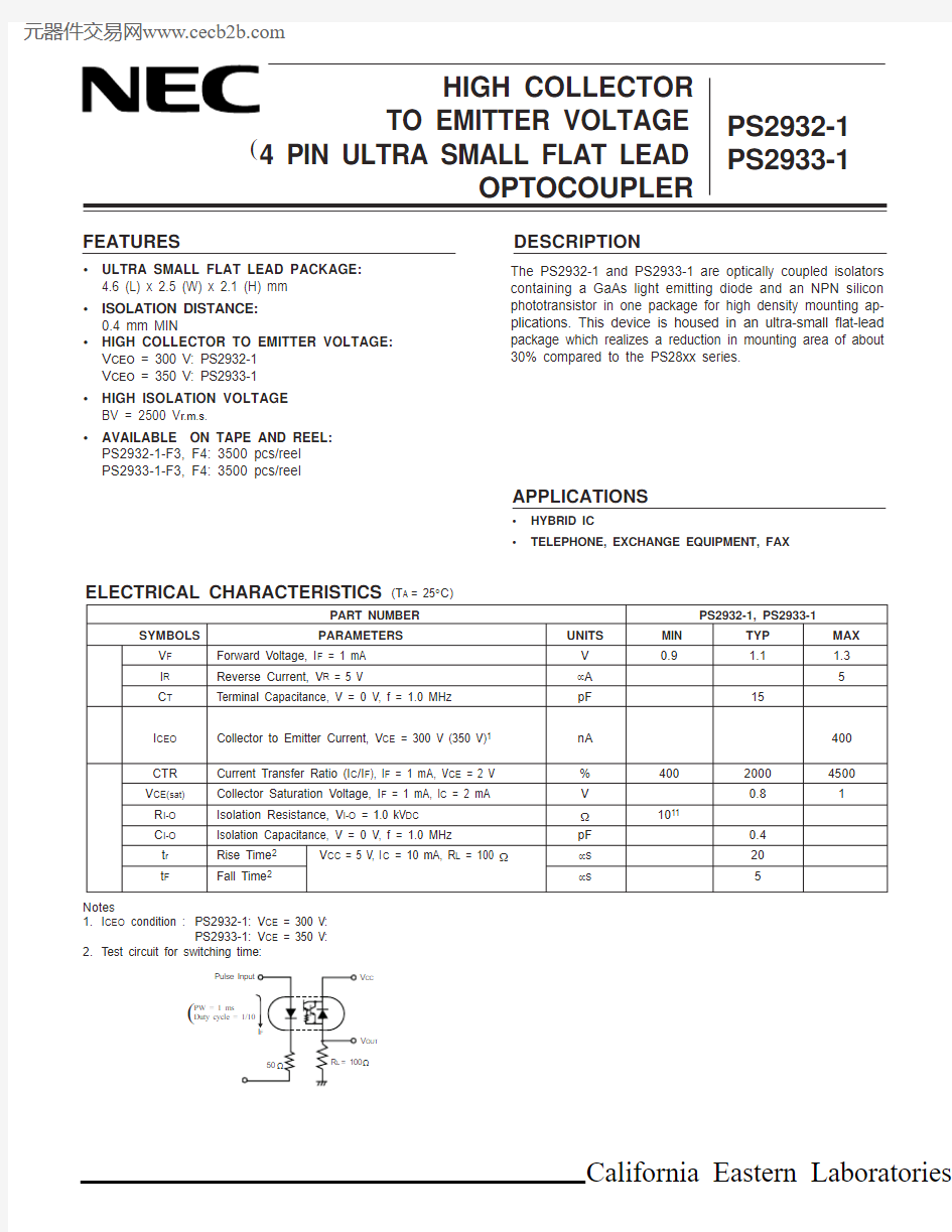
PART NUMBER
PS2932-1, PS2933-1
SYMBOLS
PARAMETERS
UNITS MIN TYP MAX V F Forward Voltage, I F = 1 mA V 0.9
1.1
1.3I R Reverse Current, V R = 5 V
μA 5
C T Terminal Capacitance, V = 0 V, f = 1.0 MHz pF 15
I CEO Collector to Emitter Current, V CE = 300 V (350 V)1nA 400CTR Current Transfer Ratio (I C /I F ), I F = 1 mA, V CE = 2 V %400
20004500V CE(sat)
Collector Saturation Voltage, I F
= 1 mA, I C = 2 mA V 0.81
R I-O Isolation Resistance, V I-O = 1.0 kV DC ?1011
C I-O Isolation Capacitance, V = 0 V, f = 1.0 MHz pF 0.4t r Rise Time 2V CC = 5 V, I C = 10 mA, R L = 100 ?
μs 20t F
Fall Time 2
μs
5
ELECTRICAL CHARACTERISTICS (T A = 25°C)
T r a n s i s t o r D i o d e
C o u p l e d California Eastern Laboratories
DESCRIPTION
The PS2932-1 and PS2933-1 are optically coupled isolators containing a GaAs light emitting diode and an NPN silicon phototransistor in one package for high density mounting ap-plications. This device is housed in an ultra-small flat-lead package which realizes a reduction in mounting area of about 30% compared to the PS28xx series.
APPLICATIONS
?HYBRID IC
?
TELEPHONE, EXCHANGE EQUIPMENT, FAX
Notes
1.I CEO condition :PS2932-1: V CE = 300 V:
PS2933-1: V CE = 350 V:
2.Test circuit for switching time:
V OUT
V CC
?
PW = 1 ms
(
(
ABSOLUTE MAXIMUM RATINGS 1
(T A = 25°C unless otherwise specified)PS2932-1, PS2933-1
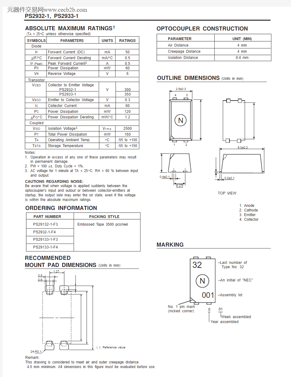
OUTLINE DIMENSIONS (Units in mm)
N 32
001
–Last number of Type No: 32–An initial of "NEC"
–Assembly lot
No. 1 pin mark (nicked corner)
01
Week assembled Year assembled
MARKING
OPTOCOUPLER CONSTRUCTION
PARAMETER UNIT (MIN)Air Distance 4 mm Creepage Distance 4 mm Isolation Distance
0.4 mm
1. Anode
2. Cathode
3. Emitter
4. Collector
SYMBOLS PARAMETERS UNITS RATINGS
Diode I F Forward Current (DC)mA 50
?IF/°C Forward Current Derating mA/°C 0.5I F
(Peak)Peak Forward Current
2A 0.5P D
Power Dissipation mW 60V R
Reverse Voltage
V
6
Transistor V CEO Collector to Emitter Voltage
PS2932-1V 300PS2933-1
350V ECO
Emitter to Collector Voltage V
0.3I C Collector Current mA
60P C Power Dissipation
mW 120?P C /?C Power Dissipation Derating mW/?C 1.2
Coupled V ISO Isolation Voltage 3V r.m.s.2500P T Total Power Dissipation mW 160T A Operating Ambient Temp.°C -55 to +100T STG Storage Temperature
°C
-55 to +150
Notes:
1.Operation in excess of any one of these parameters may result
in permanent damage.
2.PW = 100 μs, Duty Cycle = 1%.
3.AC voltage for 1 minute at TA = 25°C, RH = 60 % between input and output.CAUTIONS REGARDING NOISE:
Be aware that when voltage is applied suddenly between the optocoupler's input and outout or between collector-emitters at startup, the output side may enter the on state, even if the voltage is within the absolute maximum ratings.
PART NUMBER PACKING STYLE
PS29132-1-F3Embossed Tape 3500 pcs/reel
PS2932-1-F4PS29133-1-F3PS29133-1-F4
ORDERING INFORMATION
2
TOP VIEW
( ): Reference value
RECOMMENDED
MOUNT PAD DIMENSIONS (Units in mm)
Remark:
This drawing is considered to meet air and outer creepage distance
4.0 mm minimum. All simensions in this figure must be evaluated before use.
PS2932-1, PS2933-1
TYPICAL CHARACTERISTICS (T A = 25°C, unless otherwise specified)
100
10
10.7
0.80.9 1.0
80
60
40
20
025*******
1000255075100125
120140
1008060
4020
1.2 mW/°C
100
10
1
0.1
0.01
0.0
0.5 1.0 1.5 2.0
60
50
40
30
20
10
012345
M a x i m u m F o r w a r d C u r r e n t , I F (m A )
Ambient Temperature, T A (°C)Ambient Temperature, T A (°C)
T r a n s i s t o r P o w e r D i s s i p a t i o n , P C (m W )
Forward Voltage, V F (V)
F o r w a r d C u r r e n t , I F (m A )
C o l l e c t o r C u r r e n t , I C (V )
Collector to Emitter Voltage, V CE (V)
CollectorSaturation Voltage, V CE(sat) (V)
C o l l e c t o r C u r r e n t , I C (m A )
Ambient Temperature, T A (°C)C o l l e c t o r t o E m i t t e r D a r k C u r r e n t , I C E O (n A )
MAXIMUM FORWARD CURRENT vs. AMBIENT TEMPERATURE
TRANSISTOR POWER DISSIPATION
vs. AMBIENT TEMPERATURE
FORWARD CURRENTvs.
FORWARD VOLTAGE
COLLECTOR CURRENTvs.
COLLECTOR TO EMITTER VOLTAGE
COLLECTOR TO EMITTER DARK CURRENT
vs. AMBIENT TEMPERATURE COLLECTOR CURRENT vs.
COLLECTOR SATURATION VOLTAGE
100
1元器件交易网https://www.360docs.net/doc/aa3181962.html,
PS2932-1, PS2933-1
TYPICAL CHARACTERISTICS (T A = 25°C, unless otherwise specified)
Normalized to 1.0at T A = 25°C,
I F = 1 mA, V CE = 2 V
1.41.21.0
0.8
0.60.40.20.0-50
-25
25
50
75
100
1.2
1.0
0.8
0.6
0.4
0.2
0.0
6
Time (Hr)
C T R (r e l a t i v e V a l u e )
Load Resistance, R L (?)
S w i t c h i n g T i m e , t (μs )
Forward Current, I F (mA)
C u r r e n t T r a n s f e r R a t i o , C T R (%)
Ambient Temperature, T A (°C)N o r m a l i z e d C u r r e n t T r a n s f e r R a t i o , C T R
NORMALIZED CURRENT TRANSFER RATIO
vs. AMBIENT TEMPERATURE
CURRENT TRANSFER RATIO vs. FORWARD CURRENT
SWITCHING TIME vs. LOAD RESISTANCE
LONG TERM CTR DEGRADATION
4000
3500300025002000500015001000
REMARK: The graphs indicate nominal characteristics.
1000
100
10
0.11
元器件交易网https://www.360docs.net/doc/aa3181962.html,
TAPING SPECIFICATIONS (Units in mm)
flange
Tape Direction
Reel Outline and Dimensions
PS2932-1, PS2933-1
N N N N
N N N N
PS2932-1-F3 PS2932-1-F4PS2933-1-F3
PS2933-1-F4
Tape Outline and Dimensions
元器件交易网https://www.360docs.net/doc/aa3181962.html,
EXCLUSIVE NORTH AMERICAN AGENT FOR NEC RF, MICROWAVE & OPTOELECTRONIC SEMICONDUCTORS
? Headquarters ? 4590 Patrick Henry Drive ? Santa Clara, CA 95054-1817 ? (408) 988-3500 ? Telex 34-6393 ? FAX (408) 988-0279
Internet: https://www.360docs.net/doc/aa3181962.html,
02/06/2002
Life Support Applications
These NEC products are not intended for use in life support devices, appliances, or systems where the malfunction of these products can reasonably be expected to result in personal injury. The customers of CEL using or selling these products for use in such applications do so at their own risk and agree to fully indemnify CEL for all damages resulting from such improper use or sale.
RECOMMENDED SOLDERING CONDITIONS
(1) Infrared reflow soldering ?Peak reflow temperature 260 ?C or below (package surface temperature)?Time of peak reflow temperature 10 seconds or less ?Time of temperature higher than 220 ?C 60 seconds or less ?Time to preheat temperature from 120 to 180°C 120±30 s ?Number of reflows Three
?Flux
Rosin flux containing small amount of chlorine (The flux with a maximum chlorine content of 0.2 Wt % is recommended).
(2) Wave soldering ?Temperature 260 ?C or below (molten solder temperature)?Time
10 seconds or less
?Preheating conditions 120°C or below (package surface temperature)
?Number of times One (Allowed to be dipped in solder including plastic mold portion.)?Flux
Rosin flux containing small amount of chlorine (The flux
with a maximum chlorine content of 0.2 Wt % is recommended).
(3) Cautions ? Fluxes
Avoid removing the residual flux with chlorine-based cleaning solvent after a reflow process.
USAGE CAUTIONS
1. Protect against static electricity when handling.
2. Avoid storage at a high temperature ad high humidity.
PS2932-1, PS2933-1
Time (s)
P a c k a g e S u r f a c e T e m p e r a t u r e T (?C )
元器件交易网https://www.360docs.net/doc/aa3181962.html,