74LVX16374T中文资料
1/10
February 2003s
HIGH SPEED:
f MAX =160MHz (TYP .)at V CC =3V s 5V TOLERANT INPUTS
s POWER DOWN PROTECTION ON INPUTS s
INPUT VOLTAGE LEVEL:
V IL =0.8V,V IH =2V at V CC =3V s
LOW POWER DISSIPATION:I CC =4μA (MAX.)at T A =25°C s
LOW NOISE:
V OLP =0.3V (TYP .)at V CC =3.3V
s
SYMMETRICAL OUTPUT IMPEDANCE:|I OH |=I OL =4mA (MIN)at V CC =3V s
BALANCED PROPAGATION DELAYS:t PLH ?t PHL
s
OPERATING VOLTAGE RANGE:
V CC (OPR)=2V to 3.6V (1.2V Data Retention)s
PIN AND FUNCTION COMPATIBLE WITH 74SERIES 16373
s
IMPROVED LATCH-UP IMMUNITY
DESCRIPTION
The 74LVX16374is a low voltage CMOS 16BIT D-TYPE FLIP-FLOP with 3STATE OUTPUTS NON INVERTING fabricated with sub-micron silicon gate and double-layer metal wiring C 2MOS technology.It is ideal for low power,battery operated and low noise 3.3V applications.
These 16bit D-TYPE flip-flop is controlled by two clock inputs (CK)and two output enable inputs (nOE).The device can be used as two 8-bit flip-flops or one 16-bit flip-flop.On the positive transition of the clock,the Q outputs will be set to the logic state that were setup at the D inputs.While the (OE)input is low,the outputs will be in a normal logic state (high or low logic level);while OE is high,the outputs will be in a high impedance state.The output control does not affect the inter-nal operation of flip-flops;that is,the old data can be retained or the new data can be entered even while the outputs are off.Power down protection is provided on all inputs and 0to 7V can be accepted on inputs with no regard to the supply voltage.This device can be used to interface 5V to 3V.All in-puts and outputs are equipped with protection cir-cuits against static discharge,giving them 2KV ESD immunity and transient excess voltage.
74LVX16374
LOW VOLTAGE CMOS 16-BIT D-TYPE FLIP FLOP (3-STATE)
WITH 5V TOLERANT
INPUTS
ORDER CODES
PACKAGE TUBE
T &R
TSSOP
74LVX16374TTR
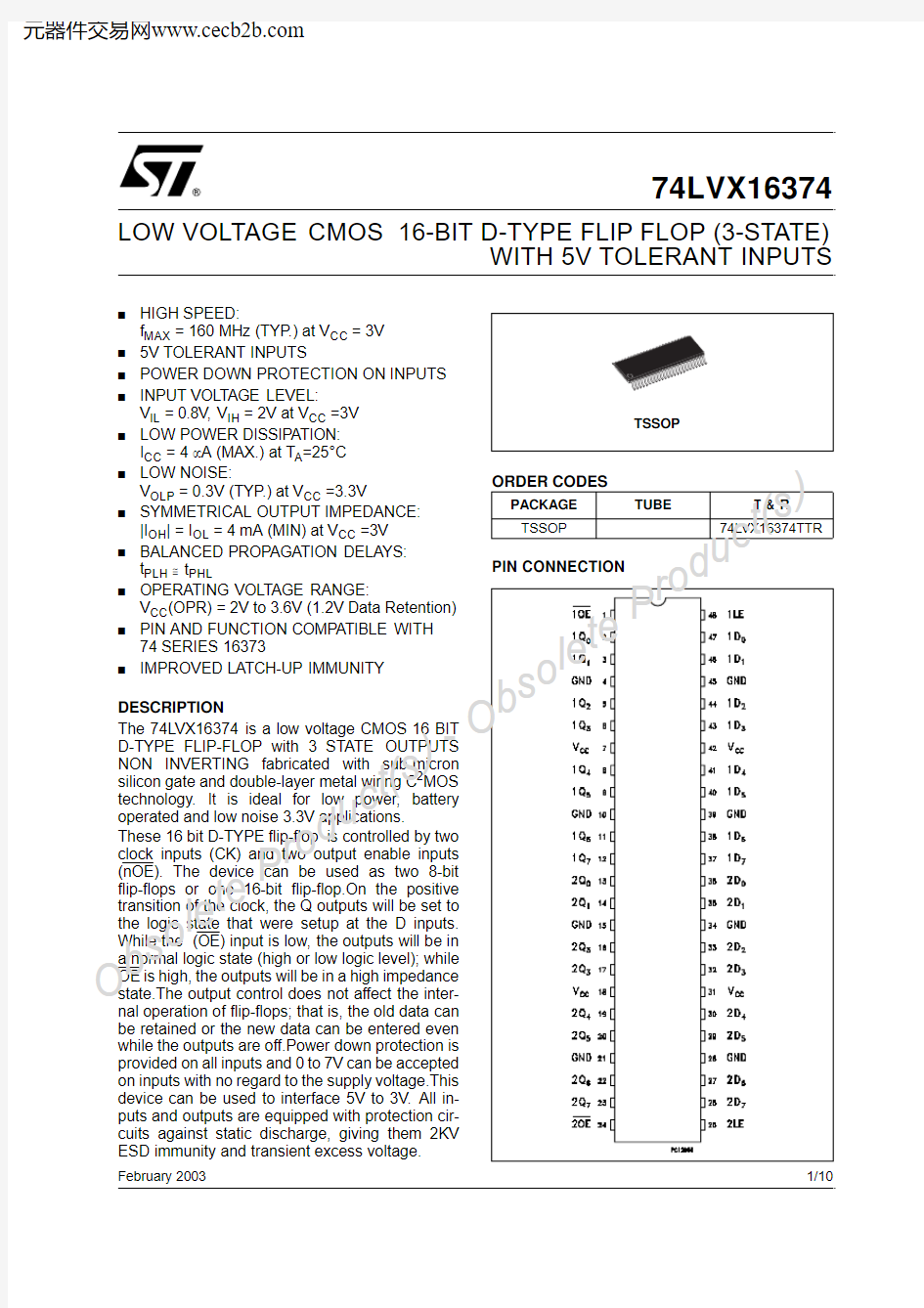
PIN CONNECTION
O
b s
o l e t e
P
r o
d u c t (s ) -
d u c t (s
)
d u c t (s ) -
74LVX16374
2/10
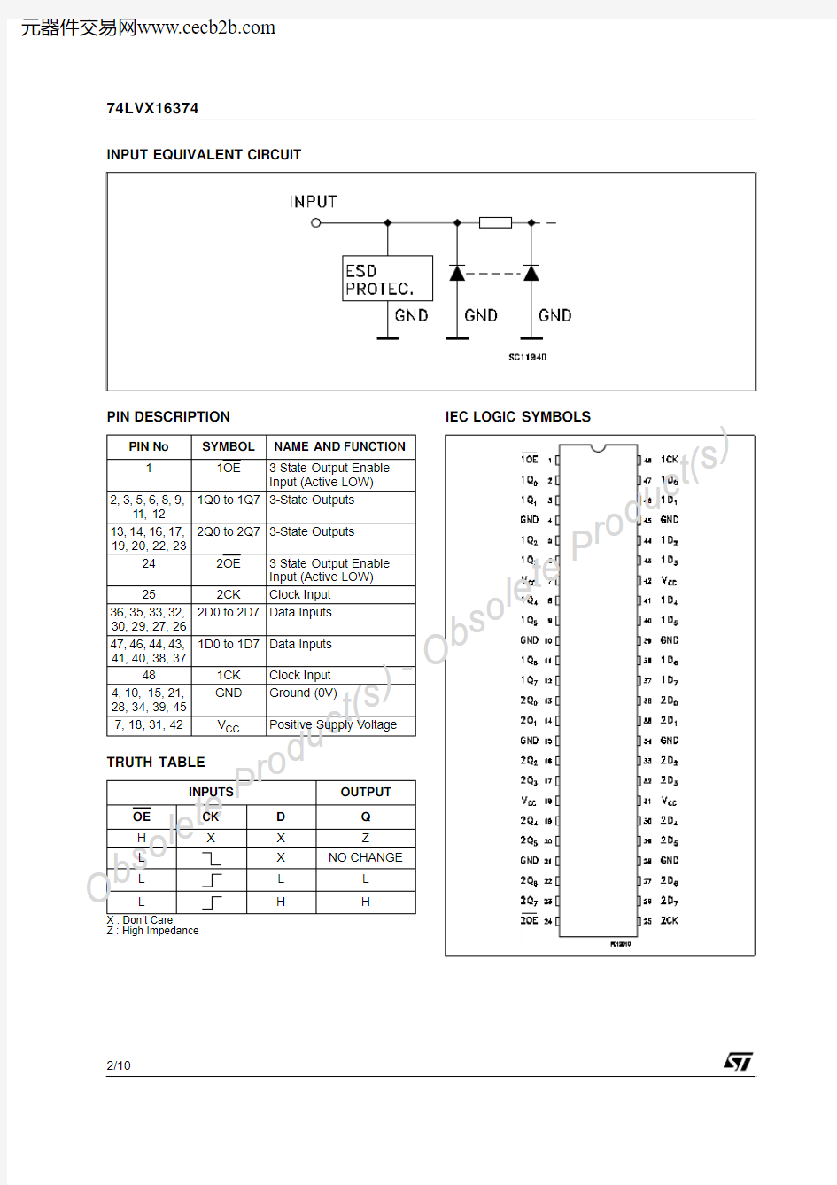
INPUT EQUIVALENT CIRCUIT
PIN DESCRIPTION
TRUTH TABLE
Z :High Impedance
IEC LOGIC SYMBOLS
PIN No SYMBOL NAME AND FUNCTION
1
1OE
3State Output Enable Input (Active LOW)
2,3,5,6,8,9,11,12
1Q0to 1Q73-State Outputs
13,14,16,17,19,20,22,23
2Q0to 2Q73-State Outputs 242OE
3State Output Enable Input (Active LOW)
252CK Clock Input 36,35,33,32,30,29,27,26
2D0to 2D7Data Inputs 47,46,44,43,41,40,38,37
1D0to 1D7Data Inputs 481CK Clock Input 4,10,15,21,28,34,39,45GND Ground (0V)7,18,31,42V CC Positive Supply Voltage
O
b s
o
l e t e
P
r o
d u c t (s )
- O b
s o l e t e
P r o
d u c
74LVX16374
3/10
LOGIC DIAGRAM
ABSOLUTE MAXIMUM RATINGS
Absolute Maximum Ratings are those values beyond which damage to the device may occur.Functional operation under these conditions is
not implied
RECOMMENDED OPERATING CONDITIONS
1)Truth Table guaranteed:1.2V to 3.6V 2)V IN from 0.8V to 2.0V
Symbol Parameter
Value Unit V CC Supply Voltage -0.5to +7.0V V I DC Input Voltage -0.5to +7.0
V V O DC Output Voltage -0.5to V CC +0.5
V I IK DC Input Diode Current -20
mA I OK DC Output Diode Current ±20mA I O
DC Output Current
±25mA I CC or I GND DC V CC or Ground Current
±50
mA T stg
Storage Temperature -65to +150
°C T L
Lead Temperature (10sec)
300
°C
Symbol Parameter Value Unit V CC Supply Voltage (note 1)2to 3.6V V I
Input Voltage 0to 5.5V V O
Output Voltage 0to V CC V T op
Operating Temperature
-55to 125°C dt/dv
Input Rise and Fall Time (note 2)(V CC =3V)
0to 100
ns/V
O
b s
o l e t e
P
r o
d u c t (s ) -
O b
s o l e t e
P r o
d u c t (s
) 74LVX16374
4/10
DC SPECIFICATIONS
DYNAMIC SWITCHING CHARACTERISTICS
1)Worst case package.
2)Max number of outputs defined as (n).Data inputs are driven 0V to 3.3V,(n-1)outputs switching and one output at GND.
3)Max number of data inputs (n)switching.(n-1)switching 0V to 3.3V.Inputs under test switching:3.3V to threshold (V ILD ),0V to threshold (V IHD ),f=1MHz.
Symbol
Parameter
Test Condition
Value Unit
V CC (V)T A =25°C -40to 85°C -55to 125°C Min.Typ.
Max.
Min.Max.
Min.Max.
V IH
High Level Input Voltage 2.0 1.5 1.5 1.5V 3.0 2.0 2.0 2.03.6 2.4
2.4
2.4
V IL
Low Level Input Voltage
2.00.50.50.5V
3.00.80.80.83.60.8
0.8
0.8V OH
High Level Output Voltage
2.0I O =-50μA 1.9 2.0 1.9 1.9V
3.0I O =-50μA 2.9 3.0
2.9 2.9
3.0
I O =-4mA 2.58
2.48
2.4
V OL
Low Level Output Voltage
2.0I O =50μA 0.00.10.10.1V
3.0I O =50μA 0.0
0.10.10.1
3.0
I O =4mA 0.360.44
0.55
I OZ High Impedance Output Leakage Current
3.6V I =V IH or V IL V O =V CC or GND ±0.25±2.5±2.5μA I I Input Leakage Current
3.6V I =5V or GND ±0.1±1±1μA I CC
Quiescent Supply Current
3.6
V I =V CC or GND
4
40
40
μA
Symbol
Parameter
Test Condition
Value Unit
V CC
(V)T A =25°C -40to 85°C
-55to 125°C Min.Typ.Max.Min.
Max.
Min.
Max.
V OLP Dynamic Low Voltage Quiet Output (note 1,2) 3.3C L =50pF
0.30.8
V
V OLV -0.8-0.3
V IHD Dynamic High Voltage Input (note 1,3) 3.3 2.0
V ILD
Dynamic Low Voltage Input (note 1,3)
3.3
0.8
O
b s
o l e t e
P
r o
d u c t (s )
- O b
s o l e t e
P r o
d u c t (s
) 74LVX16374
5/10
AC ELECTRICAL CHARACTERISTICS (Input t r =t f =3ns)
1)Skew is defined as the absolute value of the difference between the actual propagation delay for any two outputs of the same device switch-ing in the same direction,either HIGH or LOW 2)Parameter guaranteed by design (*)Voltage range is 3.3V ±0.3V
CAPACITIVE CHARACTERISTICS
1)C PD is defined as the value of the IC’s internal equivalent capacitance which is calculated from the operating current consumption without load.(Refer to Test Circuit).Average operating current can be obtained by the following equation.I CC(opr)=C PD x V CC x f IN +I CC /16(per circuit)
Symbol
Parameter
Test Condition
Value Unit
V CC (V)C L (pF)T A =25°C -40to 85°C -55to 125°C Min.
Typ.Max.Min.Max.Min.Max.t PLH t PHL
Propagation Delay Time CK to Q
2.7159.516.3 1.019.5 1.020.5ns 2.75011.019.8 1.02
3.0 1.02
4.03.3(*)
159151171173.3(*)5010.616.2118.5118.5t PZL t PZH
Output Enable Time
2.7158.614.5 1.017.5 1.018.5ns
2.75010.118.0 1.021.0 1.022.0
3.3(*)
158131151153.3(*)509.614.9116116t PLZ t PHZ Output Disable Time
2.75011.518.5 1.022.0 1.02
3.0ns 3.3(*)509.6
13.2
1.015.0
1.016.0t W CK pulse Width,HIGH
2.7505555ns
3.3(*)505555
t S Setup Time D to CK HIGH or LOW 2.750 4.54
4ns 3.3(*)5033
3t h Hold Time D to CK HIGH or LOW 2.750222
ns
3.3(*)50222f MAX
Maximum Clock Frequency
2.71560115
5045MHz
2.75045604035
3.3(*)
15100
16085753.3(*)5080
13070
70
80t OSLH t OSHL
Output to Output Skew Time (note 1,2)
2.7500.5 1.0
1.5 1.5ns
3.3(*)
50
0.5
1.0
1.5
1.5
Symbol
Parameter
Test Condition
Value Unit
V CC
(V)
T A =25°C -40to 85°C -55to 125°C Min.
Typ.Max.Min.
Max.Min.
Max.C IN
Input Capacitance 2.510
10
10
pF C OUT Output
Capacitance
4
pF C PD
Power Dissipation Capacitance (note 1)
3.0
f IN =10MHz
17
pF
l e t e
P r o
d u c t (s
) 74LVX16374
6/10
TEST CIRCUIT
C L =15/50pF or equivalent (includes jig and probe capacitance)R L =R1=1K ? or equivalent
R T =Z OUT of pulse generator (typically 50?)
WAVEFORM 1PROPAGATION DELAYS,SETUP AND HOLD TIMES,MAXIMUM CLOCK FREQUENCY (f=1MHz;50%duty cycle)
TEST
SWITCH t PLH ,t PHL Open t PZL ,t PLZ V CC t PZH ,t PHZ
GND
74LVX16374 WAVEFORM2:OUTPUT ENABLE AND DISABLE TIME(f=1MHz;50%duty cycle)
WAVEFORM3:CLOCK PULSE WIDTH(f=1MHz;50%duty cycle)
7/10
O
b s
o l e t e
P
r o
d u c t (s ) -
O b
s o l e t e
P r o
d u c t (s
) 74LVX16374
10/10
Information furnished is believed to be accurate and reliable. However, STMicroelectronics assumes no responsibility for the consequences of use of such information nor for any infringement of patents or other rights of third parties which may result from its use. No license is granted by implication or otherwise under any patent or patent rights of STMicroelectronics. Specifications mentioned in this publication are subject to change without notice. This publication supersedes and replaces all information previously supplied. STMicroelectronics products are not authorized for use as critical components in life support devices or systems without express written approval of STMicroelectronics.
? The ST logo is a registered trademark of STMicroelectronics ? 2003 STMicroelectronics - Printed in Italy - All Rights Reserved
STMicroelectronics GROUP OF COMPANIES
Australia - Brazil - Canada - China - Finland - France - Germany - Hong Kong - India - Israel - Italy - Japan - Malaysia - Malta - Morocco
Singapore - Spain - Sweden - Switzerland - United Kingdom - United States.
? https://www.360docs.net/doc/ad17189300.html,