cd4067b PDF芯片资料
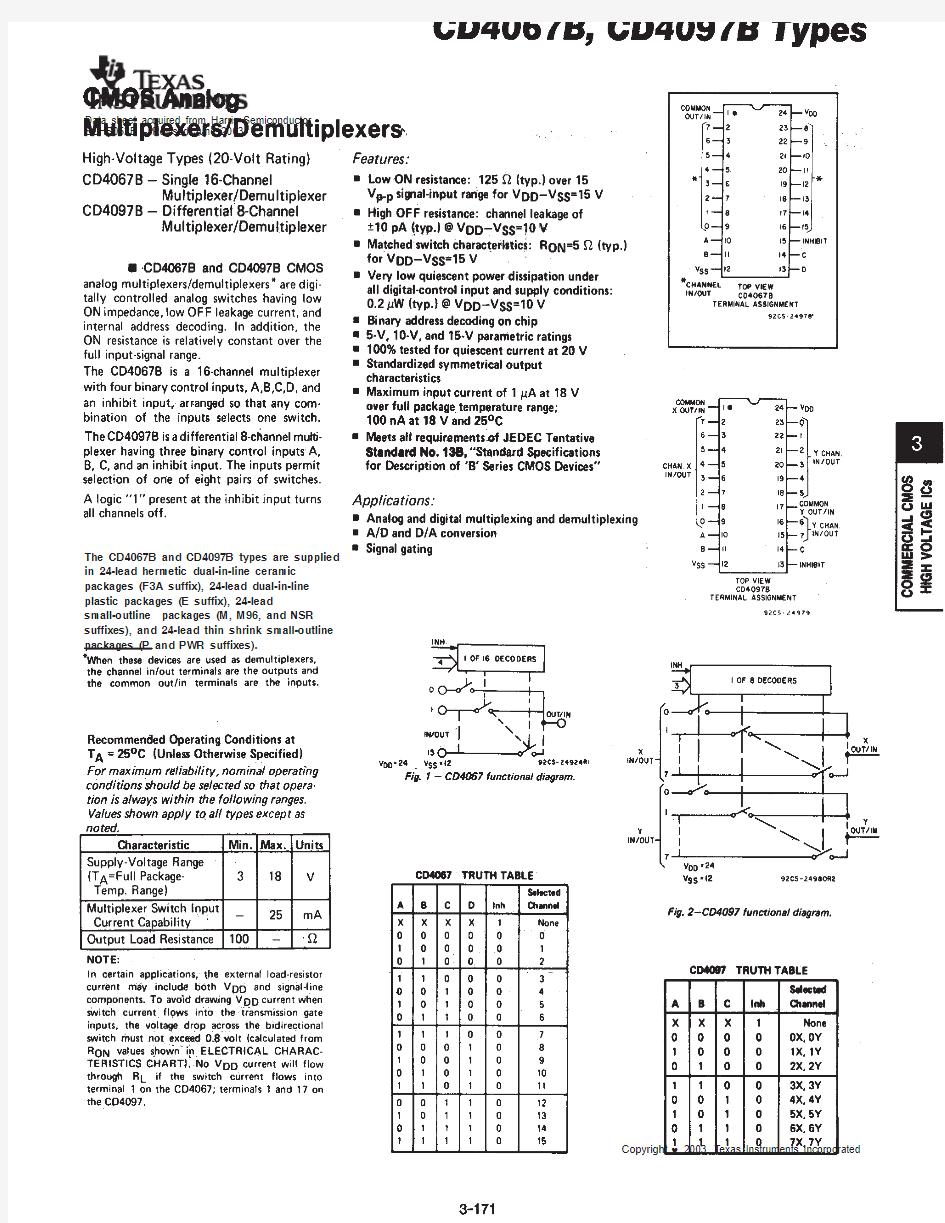

The CD4067B and CD4097B types are supplied in 24-lead hermetic dual-in-line ceramic packages (F3A suffix), 24-lead dual-in-line plastic packages (E suffix), 24-lead small-outline packages (M, M96, and NSR suffixes), and 24-lead thin shrink small-outline packages (P and PWR suffixes).
PACKAGING INFORMATION
Addendum-Page 1
(1) The marketing status values are defined as follows:
ACTIVE: Product device recommended for new designs.
LIFEBUY: TI has announced that the device will be discontinued, and a lifetime-buy period is in effect.
NRND: Not recommended for new designs. Device is in production to support existing customers, but TI does not recommend using this part in a new design.
PREVIEW: Device has been announced but is not in production. Samples may or may not be available.
OBSOLETE: TI has discontinued the production of the device.
(2) Eco Plan - The planned eco-friendly classification: Pb-Free (RoHS), Pb-Free (RoHS Exempt), or Green (RoHS & no Sb/Br) - please check https://www.360docs.net/doc/a918398811.html,/productcontent for the latest availability information and additional product content details.
TBD: The Pb-Free/Green conversion plan has not been defined.
Pb-Free (RoHS): TI's terms "Lead-Free" or "Pb-Free" mean semiconductor products that are compatible with the current RoHS requirements for all 6 substances, including the requirement that lead not exceed 0.1% by weight in homogeneous materials. Where designed to be soldered at high temperatures, TI Pb-Free products are suitable for use in specified lead-free processes.
Pb-Free (RoHS Exempt): This component has a RoHS exemption for either 1) lead-based flip-chip solder bumps used between the die and package, or 2) lead-based die adhesive used between the die and leadframe. The component is otherwise considered Pb-Free (RoHS compatible) as defined above.
Green (RoHS & no Sb/Br): TI defines "Green" to mean Pb-Free (RoHS compatible), and free of Bromine (Br) and Antimony (Sb) based flame retardants (Br or Sb do not exceed 0.1% by weight in homogeneous material)
(3) MSL, Peak Temp. - The Moisture Sensitivity Level rating according to the JEDEC industry standard classifications, and peak solder temperature.
(4) There may be additional marking, which relates to the logo, the lot trace code information, or the environmental category on the device.
(5) Multiple Device Markings will be inside parentheses. Only one Device Marking contained in parentheses and separated by a "~" will appear on a device. If a line is indented then it is a continuation of the previous line and the two combined represent the entire Device Marking for that device.
(6) Lead/Ball Finish - Orderable Devices may have multiple material finish options. Finish options are separated by a vertical ruled line. Lead/Ball Finish values may wrap to two lines if the finish value exceeds the maximum column width.
Important Information and Disclaimer:The information provided on this page represents TI's knowledge and belief as of the date that it is provided. TI bases its knowledge and belief on information provided by third parties, and makes no representation or warranty as to the accuracy of such information. Efforts are underway to better integrate information from third parties. TI has taken and continues to take reasonable steps to provide representative and accurate information but may not have conducted destructive testing or chemical analysis on incoming materials and chemicals. TI and TI suppliers consider certain information to be proprietary, and thus CAS numbers and other limited information may not be available for release.
Addendum-Page 2
In no event shall TI's liability arising out of such information exceed the total purchase price of the TI part(s) at issue in this document sold by TI to Customer on an annual basis.
OTHER QUALIFIED VERSIONS OF CD4067B, CD4067B-MIL, CD4097B, CD4097B-MIL :
?Catalog: CD4067B, CD4097B
?Military: CD4067B-MIL, CD4097B-MIL
NOTE: Qualified Version Definitions:
?Catalog - TI's standard catalog product
?Military - QML certified for Military and Defense Applications
Addendum-Page 3
TAPE AND REEL INFORMATION
*All dimensions are nominal Device Package Type Package Drawing
Pins
SPQ Reel Diameter (mm)Reel Width W1(mm)A0(mm)B0(mm)K0(mm)P1(mm)W (mm)Pin1Quadrant CD4067BM96SOIC
DW 242000330.024.410.7515.7 2.712.024.0Q1CD4067BM96SOIC
DW 242000330.024.410.7515.7 2.712.024.0Q1CD4067BM96G4SOIC
DW 242000330.024.410.7515.7 2.712.024.0Q1CD4067BPWR TSSOP
PW 242000330.016.4 6.958.3 1.68.016.0Q1CD4097BPWR TSSOP PW 242000
330.016.4 6.958.3 1.68.016.0Q1
*All dimensions are nominal
Device Package Type Package Drawing Pins SPQ Length(mm)Width(mm)Height(mm) CD4067BM96SOIC DW242000366.0364.050.0 CD4067BM96SOIC DW242000367.0367.045.0 CD4067BM96G4SOIC DW242000367.0367.045.0 CD4067BPWR TSSOP PW242000367.0367.038.0
CD4097BPWR TSSOP PW242000367.0367.038.0
IMPORTANT NOTICE
Texas Instruments Incorporated and its subsidiaries(TI)reserve the right to make corrections,enhancements,improvements and other changes to its semiconductor products and services per JESD46,latest issue,and to discontinue any product or service per JESD48,latest issue.Buyers should obtain the latest relevant information before placing orders and should verify that such information is current and complete.All semiconductor products(also referred to herein as“components”)are sold subject to TI’s terms and conditions of sale supplied at the time of order acknowledgment.
TI warrants performance of its components to the specifications applicable at the time of sale,in accordance with the warranty in TI’s terms and conditions of sale of semiconductor products.Testing and other quality control techniques are used to the extent TI deems necessary to support this warranty.Except where mandated by applicable law,testing of all parameters of each component is not necessarily performed.
TI assumes no liability for applications assistance or the design of Buyers’products.Buyers are responsible for their products and applications using TI components.To minimize the risks associated with Buyers’products and applications,Buyers should provide adequate design and operating safeguards.
TI does not warrant or represent that any license,either express or implied,is granted under any patent right,copyright,mask work right,or other intellectual property right relating to any combination,machine,or process in which TI components or services are https://www.360docs.net/doc/a918398811.html,rmation published by TI regarding third-party products or services does not constitute a license to use such products or services or a warranty or endorsement https://www.360docs.net/doc/a918398811.html,e of such information may require a license from a third party under the patents or other intellectual property of the third party,or a license from TI under the patents or other intellectual property of TI.
Reproduction of significant portions of TI information in TI data books or data sheets is permissible only if reproduction is without alteration and is accompanied by all associated warranties,conditions,limitations,and notices.TI is not responsible or liable for such altered https://www.360docs.net/doc/a918398811.html,rmation of third parties may be subject to additional restrictions.
Resale of TI components or services with statements different from or beyond the parameters stated by TI for that component or service voids all express and any implied warranties for the associated TI component or service and is an unfair and deceptive business practice. TI is not responsible or liable for any such statements.
Buyer acknowledges and agrees that it is solely responsible for compliance with all legal,regulatory and safety-related requirements concerning its products,and any use of TI components in its applications,notwithstanding any applications-related information or support that may be provided by TI.Buyer represents and agrees that it has all the necessary expertise to create and implement safeguards which anticipate dangerous consequences of failures,monitor failures and their consequences,lessen the likelihood of failures that might cause harm and take appropriate remedial actions.Buyer will fully indemnify TI and its representatives against any damages arising out of the use of any TI components in safety-critical applications.
In some cases,TI components may be promoted specifically to facilitate safety-related applications.With such components,TI’s goal is to help enable customers to design and create their own end-product solutions that meet applicable functional safety standards and requirements.Nonetheless,such components are subject to these terms.
No TI components are authorized for use in FDA Class III(or similar life-critical medical equipment)unless authorized officers of the parties have executed a special agreement specifically governing such use.
Only those TI components which TI has specifically designated as military grade or“enhanced plastic”are designed and intended for use in military/aerospace applications or environments.Buyer acknowledges and agrees that any military or aerospace use of TI components which have not been so designated is solely at the Buyer's risk,and that Buyer is solely responsible for compliance with all legal and regulatory requirements in connection with such use.
TI has specifically designated certain components as meeting ISO/TS16949requirements,mainly for automotive use.In any case of use of non-designated products,TI will not be responsible for any failure to meet ISO/TS16949.
Products Applications
Audio https://www.360docs.net/doc/a918398811.html,/audio Automotive and Transportation https://www.360docs.net/doc/a918398811.html,/automotive
Amplifiers https://www.360docs.net/doc/a918398811.html, Communications and Telecom https://www.360docs.net/doc/a918398811.html,/communications
Data Converters https://www.360docs.net/doc/a918398811.html, Computers and Peripherals https://www.360docs.net/doc/a918398811.html,/computers
DLP?Products https://www.360docs.net/doc/a918398811.html, Consumer Electronics https://www.360docs.net/doc/a918398811.html,/consumer-apps
DSP https://www.360docs.net/doc/a918398811.html, Energy and Lighting https://www.360docs.net/doc/a918398811.html,/energy
Clocks and Timers https://www.360docs.net/doc/a918398811.html,/clocks Industrial https://www.360docs.net/doc/a918398811.html,/industrial
Interface https://www.360docs.net/doc/a918398811.html, Medical https://www.360docs.net/doc/a918398811.html,/medical
Logic https://www.360docs.net/doc/a918398811.html, Security https://www.360docs.net/doc/a918398811.html,/security
Power Mgmt https://www.360docs.net/doc/a918398811.html, Space,Avionics and Defense https://www.360docs.net/doc/a918398811.html,/space-avionics-defense Microcontrollers https://www.360docs.net/doc/a918398811.html, Video and Imaging https://www.360docs.net/doc/a918398811.html,/video
RFID https://www.360docs.net/doc/a918398811.html,
OMAP Applications Processors https://www.360docs.net/doc/a918398811.html,/omap TI E2E Community https://www.360docs.net/doc/a918398811.html,
Wireless Connectivity https://www.360docs.net/doc/a918398811.html,/wirelessconnectivity
Mailing Address:Texas Instruments,Post Office Box655303,Dallas,Texas75265
Copyright?2014,Texas Instruments Incorporated
74LS373详细资料精心整理
74LS373 引脚图、内部结构、参数、典型应用电路 【功能简介】 74LS373是一款常用的地址锁存器芯片,由八个并行的、带三态缓冲输出的D触发器构成。在单片机系统中为了扩展外部存储器,通常需要一块74LS373芯片。本文将介绍74LS373的工作原理,内容涵盖引脚图、内部结构、主要参数以及在单片机扩展系统中的典型应用电路。 【内部逻辑结构图】 74LS373地址锁存器的内部逻辑结构如图一所示。 图1
【74LS373的真值表(功能表)】 G—与8031/8051的ALE相连,控制八个D型锁存器的导通与截止:高电平时,八个D型锁存器正常运行(导通),即锁存器的输出端 与输入端D的反相信号始终同步;低电平时锁存器截止,D锁存器输出 端的状态保持不变。 OE(Output Enable = Output Control)—使能端,接地时锁存 【74LS373引脚排列图】
【74LS373电气参数】 拖动图片放大! 74ls373推荐工作条件 【74LS373在单片机扩展系统中的典型应用电路】 当74LS373用作地址锁存器时,应使OE为低电平,此时锁存使能端G为高电平时,输出Q0-Q7的状态与输入端D1-D7状态相同;当G发生负的跳变时,输入端D0-D7 数据锁入Q0-Q7。51单片机的ALE信号可以直接与74LS373的G 连接。在MCS-51单片机系统中,其连接方法如下图所示。其中输入端1D-8D接
至单片机的P0口,输出端提供的是低8位地址,G端接至单片机的地址锁存允 许信号ALE。输出允许端OE接地,表示三态输出门一直导通,可以送出地址信 号。 1D-8D为8个输入端。 1Q-8Q为8个输出端。 【说明】基础比较好的同学请直接忽略。 G是数据锁存控制端;当G=1时,锁存器输出端同输入端;当G由“1”变为“0”时,数据输入锁存器中。 OE为输出允许端;当OE=“0”时,三态门打开;当OE=“1”时,三态门关闭,输出呈高阻状态。 (1).1脚是输出使能(OE),是低电平有效,当1脚是高电平时,不管输入3、4、7、8、13、14、17、18如何,也不管11脚(锁存控制端,G)如何,输出2(Q0)、5(Q1)、6(Q2)、9(Q3)、12(Q4)、15(Q5)、16(Q6)、19(Q7)全部呈现高阻状态(或者叫浮空状态); (2).当1脚是低电平时,只要11脚(锁存控制端,G)上出现一个下降沿,输出2(Q0)、5(Q1)、6(Q2)、9(Q3)、12(Q4)、15(Q5)、16(Q6)、19(Q7)立即呈现输入脚3、4、7、8、13、14、17、18的状态. 锁存端LE 由高变低时,输出端8 位信息被锁存,直到LE 端再次有效。当三态门使能信号OE为低电平时,三态门导通,允许Q0~Q7输出,OE为高电平时,输出悬空。
74ls74中文资料
74ls74中文资料 74LS74内含两个独立的D上升沿双d触发器,每个触发器有数据输入(D)、置位输入()复位输入()、时钟输入(CP)和数据输出(Q、)。、的低电平使输出预置或清除,而与 其它输入端的电平无关。当、均无效(高电平式)时,符合建立时间要求的D数据在CP上升沿作用下传送到输出端。 74ls74功能表: 输入输出 S D R D CP D Qn+1 Qn+1 0 1 ×× 1 0 1 0 ××0 1 0 0 ××φ φ 1 1 ↑ 1 1 0 1 1 ↑0 0 1 1 1 ↓×Qn Qn 图1 74ls74引脚图 实验: 用74LS74构成4位寄存器
一个D触发器可实现一位二进数的存储,因此应采用4个D触发器实现4位寄存器。由于要实现移位寄存,4个D触发器之间应相互联接。 (1)首先在图2中完成相应的联线,构成可实现并入并出、串入串出、并入串出、串入并出的多功能移位寄存。按图接好电路。 (2) D3 D2 D1 D0分别接逻辑开关,Q3 Q2 Q1 Q0接发光二极管; (3) 先清零; (4) 按下列要求,实现相应功能,观察结果,并描述工作过程。 并入并出: 使数据输入端D3D2D1D0=1011,给CP端输入一个正单脉冲,观察Q3Q2Q1Q0发光二极管的状态,、将结果填入表中。 并入串出: 使数据输入端D3D2D1D0=1011,给CP端输入4个正单脉冲,观察Q3端发光二极管的状态,将结果填入表6中。 串入并出: 使数据输入端D0分别为1011,同时通过给CP端输入正单脉冲将D0端的4 个数据送入寄存器。观察Q3Q2Q1Q0端发光二极管的状态,将结果填入表中。 串入串出: 使数据输入端D0分别为1011,同时通过给CP端输入正单脉冲,将D0端的4 个数据送入寄存器。在CP端输完8个脉冲后,观察Q3端发光二极管的状态,将结果填入表2中。并入并出:D3D2D1D0=10111个CP脉冲Q3Q2Q1Q0=结论:并入串出D3D2D1D0=10114个CP脉冲Q3=结论 串入并出D3=10114个CP脉冲Q3Q2Q1Q0=结论 串入串出D3=10118个CP脉冲Q3=结论
DM74LS299WM中文资料
? 2000 Fairchild Semiconductor Corporation DS009827 https://www.360docs.net/doc/a918398811.html, October 1988Revised March 2000 DM74LS299 8-Input Universal Shift/Storage Register with Common Parallel I/O Pins DM74LS299 8-Input Universal Shift/Storage Register with Common Parallel I/O Pins General Description The DM74LS299 is an 8-bit universal shift/storage register with 3-STATE outputs. Four modes of operation are possi-ble: hold (store), shift left, shift right and load data. The par-allel load inputs and flip-flop outputs are multiplexed to reduce the total number of package pins. Separate outputs are provided for flip-flops Q0 and Q7 to allow easy cascad-ing. A separate active LOW Master Reset is used to reset the register.Features s Common I/O for reduced pin count s Four operation modes: shift left, shift right, load and store s Separate shift right serial input and shift left serial input for easy cascading s 3-STATE outputs for bus oriented applications Ordering Code: Devices also available in T ape and Reel. Specify by appending the suffix letter “X” to the ordering code. Logic Symbol V CC = Pin 20GND = Pin 10 Pin Descriptions Connection Diagram Order Number Package Number Package Description DM74LS299WM M20B 20-Lead Small Outline Integrated Circuit (SOIC), JEDEC MS-013, 0.300 Wide DM74LS299N N20A 20-Lead Plastic Dual-In-Line Package (PDIP), JEDEC MS-001, 0.300 Wide Pin Names Description CP Clock Pulse Input (Active Rising Edge)D S0Serial Data Input for Right Shift D S7Serial Data Input for Left Shift S0, S1Mode Select Inputs MR Asynchronous Master Reset Input (Active LOW) OE1, OE23-STATE Output Enable Inputs (Active LOW)I/O0–I/O7Parallel Data Inputs or 3-STATE Parallel Outputs Q0–Q7 Serial Outputs
74LS系列芯片引脚图资料大全
74系列芯片引脚图资料大全 作者:佚名来源:本站原创点击数:57276 更新时间:2007年07月26日【字体:大中小】 为了方便大家我收集了下列74系列芯片的引脚图资料,如还有需要请上电子论坛https://www.360docs.net/doc/a918398811.html,/b bs/ 反相器驱动器LS04 LS05 LS06 LS07 LS125 LS240 LS244 LS245 与门与非门LS00 LS08 LS10 LS11 LS20 LS21 LS27 LS30 LS38 或门或非门与或非门LS02 LS32 LS51 LS64 LS65 异或门比较器LS86 译码器LS138 LS139 寄存器LS74 LS175 LS373
反相器: Vcc 6A 6Y 5A 5Y 4A 4Y 六非门 74LS04 ┌┴—┴—┴—┴—┴—┴—┴┐六非门(OC门) 74LS05 _ │14 13 12 11 10 9 8│六非门(OC高压输出) 74LS06 Y = A )│ │ 1 2 3 4 5 6 7│ └┬—┬—┬—┬—┬—┬—┬┘ 1A 1Y 2A 2Y 3A 3Y GND 驱动器: Vcc 6A 6Y 5A 5Y 4A 4Y ┌┴—┴—┴—┴—┴—┴—┴┐ │14 13 12 11 10 9 8│ Y = A )│六驱动器(OC高压输出) 74LS07 │ 1 2 3 4 5 6 7│ └┬—┬—┬—┬—┬—┬—┬┘ 1A 1Y 2A 2Y 3A 3Y GND Vcc -4C 4A 4Y -3C 3A 3Y ┌┴—┴—┴—┴—┴—┴—┴┐ _ │14 13 12 11 10 9 8│ Y =A+C )│四总线三态门74LS125 │ 1 2 3 4 5 6 7│ └┬—┬—┬—┬—┬—┬—┬┘ -1C 1A 1Y -2C 2A 2Y GND
74LS系列芯片资料
74、74HC、74LS系列芯片资料 74、74HC、74LS系列芯片资料 系列电平典型传输延迟ns 最大驱动电流(-Ioh/Lol)mA AHC CMOS 8.5 -8/8 AHCT COMS/TTL 8.5 -8/8 HC COMS 25 -8/8 HCT COMS/TTL 25 -8/8 ACT COMS/TTL 10 -24/24 F TTL 6.5 -15/64 ALS TTL 10 -15/64 LS TTL 18 -15/24 注:同型号的74系列、74HC系列、74LS系列芯片,逻辑功能上是一样的。 74LSxx的使用说明如果找不到的话,可参阅74xx或74HCxx的使用说明。 有些资料里包含了几种芯片,如74HC161资料里包含了74HC160、74HC161、74HC162、74HC163四种芯片的资料。找不到某种芯片的资料时, 可试着查看一下临近型号的芯片资料。 7400 QUAD 2-INPUT NAND GATES与非门 7401 QUAD 2-INPUT NAND GATES OC与非门 7402 QUAD 2-INPUT NOR GATES或非门 7403 QUAD 2-INPUT NAND GATES与非门 7404 HEX INVERTING GATES反向器 7406 HEX INVERTING GATES HV高输出反向器 7408 QUAD 2-INPUT AND GATE与门 7409 QUAD 2-INPUT AND GATES OC与门 7410 TRIPLE 3-INPUT NAND GATES与非门 7411 TRIPLE 3-INPUT AND GATES与门 74121 ONE-SHOT WITH CLEAR单稳态 74132 SCHMITT TRIGGER NAND GATES 触发器与非门 7414 SCHMITT TRIGGER INVERTERS触发器反向器 74153 4-LINE TO 1 LINE SELECTOR四选一 74155 2-LINE TO 4-LINE DECODER译码器 74180 PARITY GENERATOR/CHECKER奇偶发生检验 74191 4-BIT BINARY COUNTER UP/DOWN计数器 7420 DUAL 4-INPUT NAND GATES双四输入与非门 7426 QUAD 2-INPUT NAND GATES与非门 7427 TRIPLE 3-INPUT NOR GATES三输入或非门 7430 8-INPUT NAND GATES八输入端与非门 7432 QUAD 2-INPUT OR GATES二输入或门 7438 2-INPUT NAND GATE BUFFER与非门缓冲器 7445 BCD-DECIMAL DECODER/DRIVER BCD译码驱动器
74LS系列芯片简介
74LS系列芯片简介 74ls00 2输入四与非门 74ls01 2输入四与非门 (oc) 74ls02 2输入四或非门 74ls03 2输入四与非门 (oc) 74ls04 六倒相器 74ls05 六倒相器(oc) 74ls06 六高压输出反相缓冲器/驱动器(oc,30v) 74ls07 六高压输出缓冲器/驱动器(oc,30v) 74ls08 2输入四与门 74ls09 2输入四与门(oc) 74ls10 3输入三与非门 74ls11 3输入三与门 74ls12 3输入三与非门 (oc) 74ls13 4输入双与非门 (斯密特触发) 74ls14 六倒相器(斯密特触发) 74ls15 3输入三与门 (oc) 74ls16 六高压输出反相缓冲器/驱动器(oc,15v) 74ls17 六高压输出缓冲器/驱动器(oc,15v) 74ls18 4输入双与非门 (斯密特触发) 74ls19 六倒相器(斯密特触发) 74ls20 4输入双与非门 74ls21 4输入双与门 74ls22 4输入双与非门(oc) 74ls23 双可扩展的输入或非门 74ls24 2输入四与非门(斯密特触发) 74ls25 4输入双或非门(有选通) 74ls26 2输入四高电平接口与非缓冲器(oc,15v) 74ls27 3输入三或非门 74ls28 2输入四或非缓冲器 74ls30 8输入与非门 74ls31 延迟电路 74ls32 2输入四或门 74ls33 2输入四或非缓冲器(集电极开路输出) 74ls34 六缓冲器 74ls35 六缓冲器(oc) 74ls36 2输入四或非门(有选通) 74ls37 2输入四与非缓冲器 74ls38 2输入四或非缓冲器(集电极开路输出) 74ls39 2输入四或非缓冲器(集电极开路输出) 74ls40 4输入双与非缓冲器 74ls41 bcd-十进制计数器 74ls42 4线-10线译码器(bcd输入) 74ls43 4线-10线译码器(余3码输入) 74ls44 4线-10线译码器(余3葛莱码输入) 74ls45 bcd-十进制译码器/驱动器 74ls46 bcd-七段译码器/驱动器 74ls47 bcd-七段译码器/驱动器74ls48 bcd-七段译码器/驱动器 74ls49 bcd-七段译码器/驱动器(oc) 74ls50 双二路2-2输入与或非门(一门可扩展) 74ls51 双二路2-2输入与或非门 74ls51 二路3-3输入,二路2-2输入与或非门 74ls52 四路2-3-2-2输入与或门(可扩展) 74ls53 四路2-2-2-2输入与或非门(可扩展) 74ls53 四路2-2-3-2输入与或非门(可扩展) 74ls54 四路2-2-2-2输入与或非门 74ls54 四路2-3-3-2输入与或非门 74ls54 四路2-2-3-2输入与或非门 74ls55 二路4-4输入与或非门(可扩展) 74ls60 双四输入与扩展 74ls61 三3输入与扩展 74ls62 四路2-3-3-2输入与或扩展器 74ls63 六电流读出接口门 74ls64 四路4-2-3-2输入与或非门 74ls65 四路4-2-3-2输入与或非门(oc) 74ls70 与门输入上升沿jk触发器 74ls71 与输入r-s主从触发器 74ls72 与门输入主从jk触发器 74ls73 双j-k触发器(带清除端) 74ls74 正沿触发双d型触发器(带预置端和清除端) 74ls75 4位双稳锁存器 74ls76 双j-k触发器(带预置端和清除端) 74ls77 4位双稳态锁存器 74ls78 双j-k触发器(带预置端,公共清除端和公共时钟端) 74ls80 门控全加器 74ls81 16位随机存取存储器 74ls82 2位二进制全加器(快速进位) 74ls83 4位二进制全加器(快速进位) 74ls84 16位随机存取存储器 74ls85 4位数字比较器 74ls86 2输入四异或门 74ls87 四位二进制原码/反码/oi单元 74ls89 64位读/写存储器 74ls90 十进制计数器 74ls91 八位移位寄存器 74ls92 12分频计数器(2分频和6分频) 74ls93 4位二进制计数器 74ls94 4位移位寄存器(异步) 74ls95 4位移位寄存器(并行io) 74ls96 5位移位寄存器 74ls97 六位同步二进制比率乘法器 74ls100 八位双稳锁存器 74ls103 负沿触发双j-k主从触发器(带清除端)
74ls595芯片中文资料
74595外形图 ________ QB--|1 16|--Vcc QC--|2 15|--QA QD--|3 14|--SI QE--|4 13|--/G QF--|5 12|--RCK QG--|6 11|--SCK QH--|7 10|--/SCLR GND-|8 9|--QH' |________| 74595的数据端: QA--QH: 八位并行输出端,可以直接控制数码管的8个段。 QH': 级联输出端。我将它接下一个595的SI端。 SI: 串行数据输入端。 74595的控制端说明: /SCLR(10脚): 低点平时将移位寄存器的数据清零。通常我将它接Vcc。 SCK(11脚):上升沿时数据寄存器的数据移位。QA-->QB-->QC-->...-->QH;下降沿移位寄存器数据不变。(脉冲宽度:5V时,大于几十纳秒就行了。我通常都选微秒级) RCK(12脚):上升沿时移位寄存器的数据进入数据存储寄存器,下降沿时存储寄存器数据不变。通常我将RCK置为低点平,当移位结束后,在RCK端产生一个正脉冲(5V时,大于几十纳秒就行了。我通常都选微秒级),更新显示数据。 /G(13脚): 高电平时禁止输出(高阻态)。如果单片机的引脚不紧张,用一个引脚控制它,可以方便地产生闪烁和熄灭效果。比通过数据端移位控制要省时省力。 注:74164和74595功能相仿,都是8位串行输入转并行输出移位寄存器。74164的驱动电流(25mA)比74595(35mA)的要小,14脚封装,体积也小一些。 74595的主要优点是具有数据存储寄存器,在移位的过程中,输出端的数据可以保持不变。这在串行速度慢的场合很有用处,数码管没有闪烁感。 与164只有数据清零端相比,595还多有输出端时能/禁止控制端,可以使输出为高阻态。 另外,据网上报价,贴片164每只1元钱,贴片595 0.8元/只。
74LS08中文资料
LOW POWER SCHOTTKY 14 1 PLASTIC N SUFFIX CASE 646 14 1 SOIC D SUFFIX CASE 751A
ON Semiconductor and are trademarks of Semiconductor Components Industries, LLC (SCILLC). SCILLC reserves the right to make changes without further notice to any products herein. SCILLC makes no warranty, representation or guarantee regarding the suitability of its products for any particular purpose, nor does SCILLC assume any liability arising out of the application or use of any product or circuit, and specifically disclaims any and all liability, including without limitation special, consequential or incidental damages. “Typical” parameters which may be provided in SCILLC data sheets and/or specifications can and do vary in different applications and actual performance may vary over time. All operating parameters, including “Typicals” must be validated for each customer application by customer’s technical experts. SCILLC does not convey any license under its patent rights nor the rights of others. SCILLC products are not designed, intended, or authorized for use as components in systems intended for surgical implant into the body, or other applications intended to support or sustain life, or for any other application in which the failure of the SCILLC product could create a situation where personal injury or death may occur. Should Buyer purchase or use SCILLC products for any such unintended or unauthorized application, Buyer shall indemnify and hold SCILLC and its officers, employees, subsidiaries, affiliates, and distributors harmless against all claims, costs, damages, and expenses, and reasonable attorney fees arising out of, directly or indirectly, any claim of personal injury or death associated with such unintended or unauthorized use, even if such claim alleges that SCILLC was negligent regarding the design or manufacture of the part. SCILLC is an Equal Opportunity/Affirmative Action Employer. PUBLICATION ORDERING INFORMATION ASIA/PACIFIC: LDC for ON Semiconductor – Asia Support Phone:303–675–2121 (Tue–Fri 9:00am to 1:00pm, Hong Kong Time) Toll Free from Hong Kong 800–4422–3781 Email: ONlit–asia@https://www.360docs.net/doc/a918398811.html, JAPAN: ON Semiconductor, Japan Customer Focus Center 4–32–1 Nishi–Gotanda, Shinagawa–ku, Tokyo, Japan 141–8549 Phone: 81–3–5487–8345 Email: r14153@https://www.360docs.net/doc/a918398811.html, Fax Response Line:303–675–2167
74LS系列芯片简介
红色标记为实验室有的芯片 74系列芯片的型号区别与功能略表 2010-05-31 16:39 74HC/LS/HCT/F系列芯片的区别: 1、 LS是低功耗肖特基,HC 是高速COMS。LS的速度比HC略快。HCT输入输出与LS兼容,但是功耗低;F是高速肖特基电路; 2、 LS是TTL电平,HC是COMS 电平。 3、 LS输入开路为高电平,HC输入不允许开路, hc 一般都要求有上下拉电阻来确定输入端无效时的电平。LS 却没有这个要 求 4、 LS输出下拉强上拉弱,HC上拉下拉相同。 5、工作电压不同,LS只能用5V,而HC一般为2V到6V;而HCT的工作电压一般为4.5V~5.5V。 6、电平不同。LS是TTL电平,其低电平和高电平分别为0.8和V2.4,而CMOS在工作电压为5V时分别为0.3V和3.6V,所以CMOS 可以驱动TTL,但反过来是不行的 7、驱动能力不同,LS一般高电平的驱动能力为5mA,低电平为20mA;而CMOS的高低电平均为5mA; 8、 CMOS器件抗静电能力差,易发生栓锁问题,所以CMOS的输入脚不能直接接电源。 74系列集成电路大致可分为6大类: .74××(标准型); .74LS××(低功耗肖特基); .74S××(肖特基); .74ALS××(先进低功耗肖特基); .74AS××(先进肖特基); .74F××(高速)。 近年来还出现了高速CMOS电路的74系列,该系列可分为3大类: .HC为COMS工作电平; .HCT为TTL工作电平,可与74LS系列互换使用; .HCU适用于无缓冲级的CMOS电路。 这9种74系列产品,只要后边的标号相同,其逻辑功能和管脚排列就相同。根据不同的条件和要求可选择不同类型的74系列产 品,比如电路的供电电压为3V就应选择74HC 系列的产品 系列电平典型传输延迟ns 最大驱动电流(-Ioh/Lol)mA AHC CMOS 8.5 -8/8 AHCT COMS/TTL 8.5 -8/8 HC COMS 25 -8/8 HCT COMS/TTL 25 -8/8 ACT COMS/TTL 10 -24/24 F TTL 6.5 -15/64 ALS TTL 10 -15/64 LS TTL 18 -15/24 注:同型号的74系列、74HC系列、74LS系列芯片,逻辑功能上是一样的。 74LSxx的使用说明如果找不 到的话,可参阅74xx或74HCxx的使用说明。 有些资料里包含了几种芯片,如74HC161资料里包含了74HC160、74HC161、74HC162、74HC163四种芯片的资料。找不到某种芯 片的资料时,可试着查看一下临近型号的芯片资料。 74HC的速度比4000系列快,引脚与标准74系列兼容 4000系列的好处是有的型号可工作在+15V 。新产品最好不用LS。https://www.360docs.net/doc/a918398811.html, 功能略表 74HC01 2输入四与非门 (oc) 74HC02 2输入四或非门 74HC03 2输入四与非门 (oc) 74HC04 六倒相器 74HC05 六倒相器(oc) 74HC06 六高压输出反相缓冲器/驱动器(oc,30v) 74HC07 六高压输出缓冲器/驱动器(oc,30v) 74HC08 2输入四与门 74HC09 2输入四与门(oc) 74HC10 3输入三与非门 74HC11 3输入三与门 74HC12 3输入三与非门 (oc)
SN74LS10_芯片资料
Copyright 2003, Texas Instruments Incorporated PRODUCTION DATA information is current as of publication date.
PACKAGING INFORMATION Orderable Device Status(1)Package Type Package Drawing Pins Package Qty Eco Plan(2)Lead/Ball Finish MSL Peak Temp(3) JM38510/00103BCA OBSOLETE CDIP J14None Call TI Call TI JM38510/00103BDA OBSOLETE CFP W14None Call TI Call TI JM38510/07005BCA ACTIVE CDIP J141None Call TI Level-NC-NC-NC JM38510/07005BDA ACTIVE CFP W141None Call TI Level-NC-NC-NC JM38510/30005B2A ACTIVE LCCC FK201None Call TI Level-NC-NC-NC JM38510/30005BCA ACTIVE CDIP J141None Call TI Level-NC-NC-NC JM38510/30005BDA ACTIVE CFP W141None Call TI Level-NC-NC-NC JM38510/30005SCA ACTIVE CDIP J141None Call TI Level-NC-NC-NC JM38510/30005SDA ACTIVE CFP W141None Call TI Level-NC-NC-NC SN5410J OBSOLETE CDIP J14None Call TI Call TI SN54LS10J ACTIVE CDIP J141None Call TI Level-NC-NC-NC SN54S10J ACTIVE CDIP J141None Call TI Level-NC-NC-NC SN7410N ACTIVE PDIP N1425Pb-Free (RoHS) CU NIPDAU Level-NC-NC-NC SN7410N3OBSOLETE PDIP N14None Call TI Call TI SN74LS10D ACTIVE SOIC D1450Pb-Free (RoHS)CU NIPDAU Level-2-260C-1YEAR/ Level-1-235C-UNLIM SN74LS10DR ACTIVE SOIC D142500Pb-Free (RoHS)CU NIPDAU Level-2-260C-1YEAR/ Level-1-235C-UNLIM SN74LS10N ACTIVE PDIP N1425Pb-Free (RoHS) CU NIPDAU Level-NC-NC-NC SN74LS10N3OBSOLETE PDIP N14None Call TI Call TI SN74LS10NSR ACTIVE SO NS142000Pb-Free (RoHS)CU NIPDAU Level-2-260C-1YEAR/ Level-1-235C-UNLIM SN74S10D ACTIVE SOIC D1450Pb-Free (RoHS)CU NIPDAU Level-2-260C-1YEAR/ Level-1-235C-UNLIM SN74S10N ACTIVE PDIP N1425Pb-Free (RoHS) CU NIPDAU Level-NC-NC-NC SN74S10N3OBSOLETE PDIP N14None Call TI Call TI SN74S10NSR ACTIVE SO NS142000Pb-Free (RoHS)CU NIPDAU Level-2-260C-1YEAR/ Level-1-235C-UNLIM SNJ5410J OBSOLETE CDIP J14None Call TI Call TI SNJ5410W OBSOLETE CFP W14None Call TI Call TI SNJ5410WA OBSOLETE CFP WA14None Call TI Call TI SNJ54LS10FK ACTIVE LCCC FK201None Call TI Level-NC-NC-NC SNJ54LS10J ACTIVE CDIP J141None Call TI Level-NC-NC-NC SNJ54LS10W ACTIVE CFP W141None Call TI Level-NC-NC-NC SNJ54S10FK ACTIVE LCCC FK201None Call TI Level-NC-NC-NC SNJ54S10J ACTIVE CDIP J141None Call TI Level-NC-NC-NC SNJ54S10W ACTIVE CFP W141None Call TI Level-NC-NC-NC (1)The marketing status values are defined as follows: ACTIVE:Product device recommended for new designs. LIFEBUY:TI has announced that the device will be discontinued,and a lifetime-buy period is in effect. NRND:Not recommended for new designs.Device is in production to support existing customers,but TI does not recommend using this part in a new design.
使用74LS74芯片
使用74LS74芯片,14号管脚接在_____________孔。 74LS74芯片的异步置位端 和异步复位端 接高电平时可 以悬空吗? A:可以 对于74LS192,当选用加法计数时,时钟脉冲应接到哪个引脚对于74LS161,当计数功能选 预考核题目 试题1、 驱动74LS161的时钟动作沿是____________ A:时钟上升沿 B:时钟下降沿 C:上升和下降沿都有效 D:上升沿和下降沿随机 试题2、 A:1) B:2) C:3) 试题3、 对于74LS192,当选用减法计数时,时钟脉冲应接到哪个引脚?
A:能 B:不能 试题4、 对于74LS192,当选用加法计数时,时钟脉冲应接到哪个引脚? A:1) B:2) C:3)
D:4) 试题5、对于74LS192,第14引脚CR接什么电平时,计数器清零? A:低电平 B:高电平 C:任意电平 择控制端为___________,计数器处于计数状态? 预考核题目 试题1、 A:时钟上升沿 B:时钟下降沿 C:上升和下降沿都有 效 D:上升沿和下降沿随 机 你的答案:C 错 试题2、 A:1) B:2) C:3) 你的答案:C 错 试题3、 A:能 B:不能
你的答案:B 错 试题4、 A:1) B:2) C:3) D:4) 你的答案:B 试题5、 A:低电平 B:高电平 C:任意电平 你的答案:A 错 你未通过本次考核,明天才能再进行这个实验项目的考核,通过后才可 进行实验! 增大时,输出波形的______________。 多谐振荡器的可调电阻R A A:周期增大,占空比增大 B:周期减小,占空比增大 C:周期增大,占空比减小 D:周期减小,占空比减小 试题2、555定时器的Vcc是第几管脚?GND是第几管脚? A:1脚;8脚 B:8脚;1脚
74LS系列数字芯片资料
74LS系列数字芯片资料 7400 TTL 2输入端四与非门 7401 TTL 集电极开路2输入端四与非门7402 TTL 2输入端四或非门 7403 TTL 集电极开路2输入端四与非门7404 TTL 六反相器 7405 TTL 集电极开路六反相器 7406 TTL 集电极开路六反相高压驱动器7407 TTL 集电极开路六正相高压驱动器7408 TTL 2输入端四与门 7409 TTL 集电极开路2输入端四与门 7410 TTL 3输入端3与非门 74107 TTL 带清除主从双J-K触发器 74109 TTL 带预置清除正触发双J-K触发器7411 TTL 3输入端3与门 74112 TTL 带预置清除负触发双J-K触发器7412 TTL 开路输出3输入端三与非门 74121 TTL 单稳态多谐振荡器 74122 TTL 可再触发单稳态多谐振荡器74123 TTL 双可再触发单稳态多谐振荡器74125 TTL 三态输出高有效四总线缓冲门74126 TTL 三态输出低有效四总线缓冲门7413 TTL 4输入端双与非施密特触发器74132 TTL 2输入端四与非施密特触发器74133 TTL 13输入端与非门 74136 TTL 四异或门 74138 TTL 3-8线译码器/复工器 74139 TTL 双2-4线译码器/复工器 7414 TTL 六反相施密特触发器 74145 TTL BCD—十进制译码/驱动器 7415 TTL 开路输出3输入端三与门 74150 TTL 16选1数据选择/多路开关 74151 TTL 8选1数据选择器 74153 TTL 双4选1数据选择器 74154 TTL 4线—16线译码器 74155 TTL 图腾柱输出译码器/分配器 74156 TTL 开路输出译码器/分配器 74157 TTL 同相输出四2选1数据选择器74158 TTL 反相输出四2选1数据选择器7416 TTL 开路输出六反相缓冲/驱动器74160 TTL 可预置BCD异步清除计数器74161 TTL 可予制四位二进制异步清除计数器74162 TTL 可预置BCD同步清除计数器74163 TTL 可予制四位二进制同步清除计数器
74LS395中文资料
TL F 9833DM74LS395 4-Bit Shift Register with TRI-STATE Outputs February1992 DM74LS395 4-Bit Shift Register with TRI-STATE Outputs General Description The LS395is a4-bit shift register with TRI-STATE outputs and can operate in either a synchronous parallel load or a serial shift-right mode as determined by the Select input An asynchronous active LOW Master Reset(MR)input over- rides the synchronous operations and clears the register An active LOW Output Enable(OE)input controls the TRI- STATE output buffers but does not interfere with the other operations The fourth stage also has a conventional output for linking purposes in multi-stage serial operations Features Y Shift right or parallel4-bit register Y TRI-STATE outputs Y Input clamp diodes limit high speed termination effects Y Fully CMOS and TTL compatible Connection Diagram Dual-In-Line Package TL F 9833–1 Order Number DM74LS395WM or DM74LS395N See NS Package Number M16B or N16E Logic Symbol TL F 9833–2 V CC e Pin16 GND e Pin8 Mode Select Table Operating Mode Inputs t n Outputs t n a1 MR CP S D S P n O0O1O2O3 Asynchronous Reset L X X X X L L L L Shift SET First Stage H K L H X H O0n O1n02n Shift RESET First Stage H K L L X L O0n O1n02n Parallel Load H K H X Pn P0P1P2P3 t n t n a1e Time before and after CP HIGH-to-LOW transition H e HIGH Voltage Level L e LOW Voltage Level X e Immaterial TRI-STATE is a registered trademark of National Semiconductor Corporation C1995National Semiconductor Corporation RRD-B30M115 Printed in U S A
74ls系列芯片功能介绍
74、74HC、74LS系列芯片资料 系列电平典型传输延迟ns 最大驱动电流(-Ioh/Lol)mA AHC CMOS 8.5 -8/8 AHCT COMS/TTL 8.5 -8/8 HC COMS 25 -8/8 HCT COMS/TTL 25 -8/8 ACT COMS/TTL 10 -24/24 F TTL 6.5 -15/64 ALS TTL 10 -15/64 LS TTL 18 -15/24 注:同型号的74系列、74HC系列、74LS系列芯片,逻辑功能上是一样的。74LSxx的使用说明如果找不到的话,可参阅74xx或74HCxx的使用说明。有些资料里包含了几种芯片,如74HC161资料里包含了74HC160、74HC161、74HC162、74HC163四种芯片的资料。找不到某种芯片的资料时, 可试着查看一下临近型号的芯片资料。 7400 QUAD 2-INPUT NAND GATES 与非门 7401 QUAD 2-INPUT NAND GATES OC 与非门 7402 QUAD 2-INPUT NOR GATES 或非门 7403 QUAD 2-INPUT NAND GATES 与非门 7404 HEX INVERTING GATES 反向器 7406 HEX INVERTING GATES HV 高输出反向器 7408 QUAD 2-INPUT AND GATE 与门 7409 QUAD 2-INPUT AND GATES OC 与门 7410 TRIPLE 3-INPUT NAND GATES 与非门 7411 TRIPLE 3-INPUT AND GATES 与门 74121 ONE-SHOT WITH CLEAR 单稳态 74132 SCHMITT TRIGGER NAND GATES 触发器与非门 7414 SCHMITT TRIGGER INVERTERS 触发器反向器 74153 4-LINE TO 1 LINE SELECTOR 四选一 74155 2-LINE TO 4-LINE DECODER 译码器 74180 PARITY GENERATOR/CHECKER 奇偶发生检验 74191 4-BIT BINARY COUNTER UP/DOWN 计数器 7420 DUAL 4-INPUT NAND GATES 双四输入与非门 7426 QUAD 2-INPUT NAND GATES 与非门 7427 TRIPLE 3-INPUT NOR GATES 三输入或非门 7430 8-INPUT NAND GATES 八输入端与非门 7432 QUAD 2-INPUT OR GATES 二输入或门 7438 2-INPUT NAND GATE BUFFER 与非门缓冲器 7445 BCD-DECIMAL DECODER/DRIVER BCD译码驱动器 7474 D-TYPE FLIP-FLOP D型触发器 7475 QUAD LATCHES 双锁存器