V23990-P518-C44-14

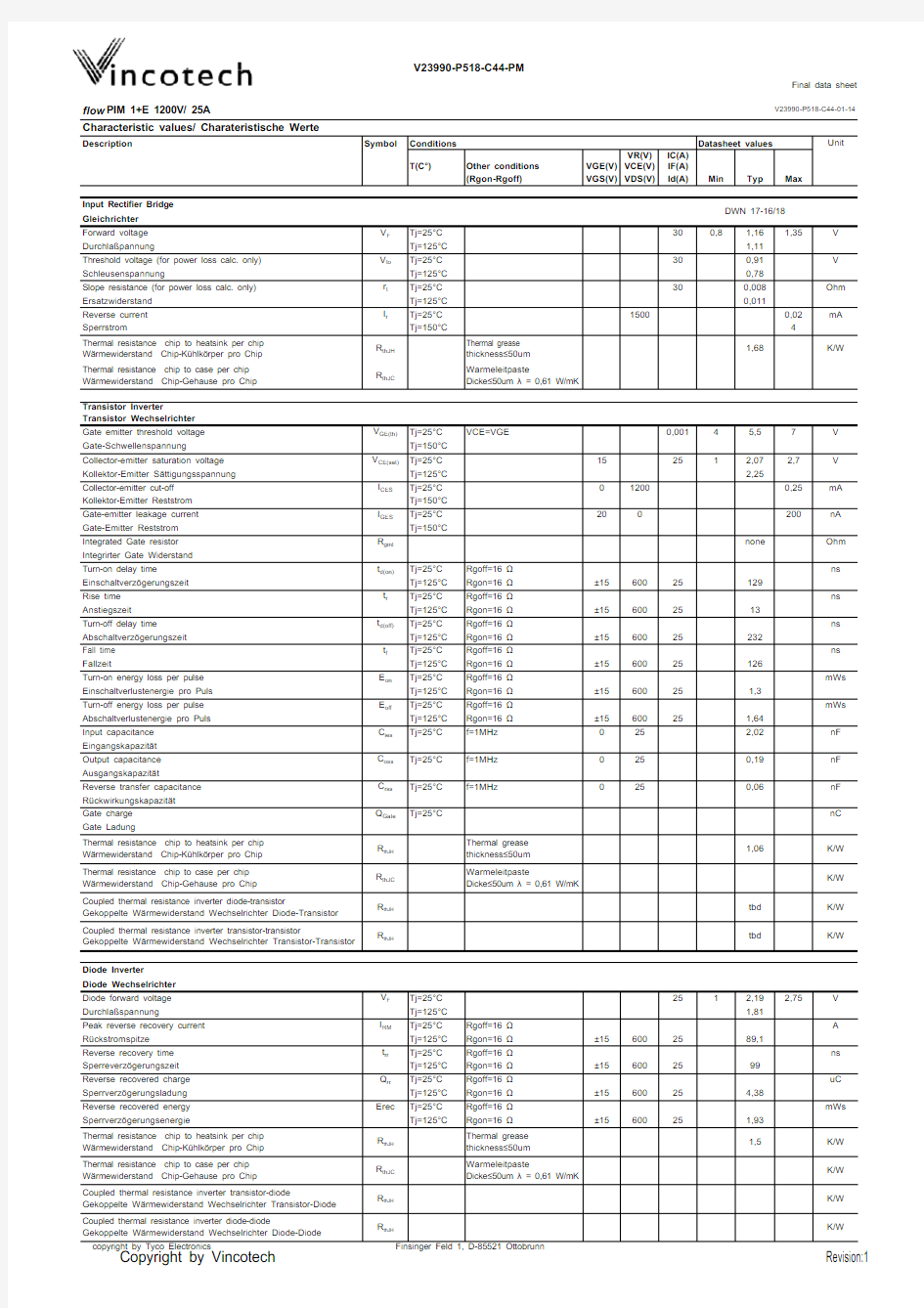
V23990-P518-C44-PM
Final data sheet
flow PIM 1+E 1200V/ 25A V23990-P518-C44-01-14 Maximum Ratings / H?chstzul?ssige Werte
Parameter Condition Symbol Datasheet values Unit
max.
Transistor Inverter
Transistor Wechselrichter
Collector-emitter break down voltage V CE1200V Kollektor-Emitter-Sperrspannung
DC collector current T j=175°C T h=80°C,I C27,3A Kollektor-Dauergleichstrom T c=80°C35,9
Repetitive peak collector current tp limited by Tj max I cpuls A Periodischer Kollektorspitzenstrom75
Power dissipation per IGBT T j=175°C T h=80°C P tot66W Verlustleistung pro IGBT T c=80°C100
Gate-emitter peak voltage V GE±20V Gate-Emitter-Spitzenspannung
SC withstand time*Tj 150°C V GE=15V t SC tbd us Kurzschlu?verhalten*V CC=360V
max. Chip temperature T jmax -55…+150°C max. Chiptemperatur
Diode Inverter
Diode Wechselrichter
DC forward current T j=175°C T h=80°C,I F26A Dauergleichstrom T c=80°C34,9
Repetitive peak forward current tp limited by Tj max I FRM A Periodischer Spitzenstrom50
Power dissipation per Diode T j=175°C T h=80°C P tot47W Verlustleistung pro Diode T c=80°C71
max. Chip temperature T jmax -55…+150°C max. Chiptemperatur
Thermal properties
Thermische Eigenschaften
Storage temperature T stg -40…+125°C Lagertemperatur
Operation temperature T op -40…+125°C Betriebstemperatur
Insulation properties
Modulisolation
Insulation voltage t=1min V is4000Vdc Isolationsspannung
Creepage distance min 12,7mm Kriechstrecke
Clearance min 12,7mm Luftstrecke
Additional notes and remarks:* Allowed number of short circuits must be less than 1000 times, and time duration
between short circuits should be more than 1 second!
V23990-P518-C44-PM
Final data sheet
flow PIM 1+E 1200V/ 25A
V23990-P518-C44-01-14
Characteristic values/ Charateristische Werte
Description
Symbol
Conditions Datasheet values
Unit
T(C°)
Other conditions VGE(V)VR(V)
VCE(V)IC(A)IF(A)(Rgon-Rgoff)
VGS(V)VDS(V)
Id(A)
Min Typ Max
Input Rectifier Bridge Gleichrichter
Forward voltage V F Tj=25°C 300,8
1,161,35
V Durchla?pannung
Tj=125°C 1,11Threshold voltage (for power loss calc. only)V to Tj=25°C 300,91V Schleusenspannung
Tj=125°C 0,78Slope resistance (for power loss calc. only)r t Tj=25°C 30
0,008Ohm
Ersatzwiderstand Tj=125°C 0,011
Reverse current I r
Tj=25°C 1500
0,02mA
Sperrstrom
Tj=150°C
4
Thermal resistance chip to heatsink per chip W?rmewiderstand Chip-Kühlk?rper pro Chip R thJH Thermal grease thickness 50um
1,68
K/W
Thermal resistance chip to case per chip W?rmewiderstand Chip-Gehause pro Chip R thJC
Warmeleitpaste
Dicke 50um ? = 0,61 W/mK
Transistor Inverter
Transistor Wechselrichter Gate emitter threshold voltage V GE(th)Tj=25°C VCE=VGE
0,00145,57V Gate-Schwellenspannung
Tj=150°C Collector-emitter saturation voltage V CE(sat)Tj=25°C 1525
1
2,072,7V Kollektor-Emitter S?ttigungsspannung Tj=125°C 2,25
Collector-emitter cut-off I CES Tj=25°C 012000,25mA Kollektor-Emitter Reststrom Tj=150°C Gate-emitter leakage current I GES Tj=25°C 20
200
nA Gate-Emitter Reststrom Tj=150°C
Integrated Gate resistor R gint none
Ohm Integrirter Gate Widerstand Turn-on delay time
t d(on)Tj=25°C Rgoff=16 ?ns
Einschaltverz?gerungszeit Tj=125°C Rgon=16 ?±1560025129
Rise time t r Tj=25°C Rgoff=16 ?ns
Anstiegszeit
Tj=125°C Rgon=16 ?±156002513
Turn-off delay time
t d(off)Tj=25°C Rgoff=16 ?ns
Abschaltverz?gerungszeit Tj=125°C Rgon=16 ?±1560025232
Fall time t f Tj=25°C Rgoff=16 ?ns
Fallzeit
Tj=125°C Rgon=16 ?±1560025126
Turn-on energy loss per pulse E on Tj=25°C Rgoff=16 ?mWs
Einschaltverlustenergie pro Puls Tj=125°C Rgon=16 ?±15600251,3
Turn-off energy loss per pulse E off Tj=25°C Rgoff=16 ?mWs
Abschaltverlustenergie pro Puls Tj=125°C Rgon=16 ?±1560025
1,64Input capacitance C ies Tj=25°C f=1MHz 0252,02nF Eingangskapazit?t Output capacitance C oss Tj=25°C f=1MHz 0250,19nF Ausgangskapazit?t
Reverse transfer capacitance C rss Tj=25°C f=1MHz
25
0,06
nF Rückwirkungskapazit?t Gate charge Q Gate
Tj=25°C
nC
Gate Ladung
Thermal resistance chip to heatsink per chip W?rmewiderstand Chip-Kühlk?rper pro Chip R thJH Thermal grease thickness 50um
1,06K/W Thermal resistance chip to case per chip W?rmewiderstand Chip-Gehause pro Chip
R thJC Warmeleitpaste
Dicke 50um ? = 0,61 W/mK K/W
Coupled thermal resistance inverter diode-transistor
Gekoppelte W?rmewiderstand Wechselrichter Diode-Transistor R thJH tbd K/W Coupled thermal resistance inverter transistor-transistor
Gekoppelte W?rmewiderstand Wechselrichter Transistor-Transistor R thJH
tbd
K/W
Diode Inverter Diode Wechselrichter Diode forward voltage V F Tj=25°C 25
1
2,192,75V Durchla?spannung
Tj=125°C 1,81Peak reverse recovery current I RM Tj=25°C Rgoff=16 ?A
Rückstromspitze
Tj=125°C Rgon=16 ?±156002589,1
Reverse recovery time t rr Tj=25°C Rgoff=16 ?ns
Sperreverz?gerungszeit Tj=125°C Rgon=16 ?±156002599
Reverse recovered charge Q rr Tj=25°C Rgoff=16 ?uC
Sperrverz?gerungsladung Tj=125°C Rgon=16 ?±15600254,38
Reverse recovered energy Erec
Tj=25°C Rgoff=16 ?mWs
Sperrverz?gerungsenergie
Tj=125°C
Rgon=16 ?±15
600
25
1,93Thermal resistance chip to heatsink per chip W?rmewiderstand Chip-Kühlk?rper pro Chip R thJH Thermal grease thickness 50um
1,5
K/W Thermal resistance chip to case per chip W?rmewiderstand Chip-Gehause pro Chip
R thJC Warmeleitpaste
Dicke 50um ? = 0,61 W/mK
K/W Coupled thermal resistance inverter transistor-diode
Gekoppelte W?rmewiderstand Wechselrichter Transistor-Diode R thJH K/W Coupled thermal resistance inverter diode-diode
DWN 17-16/18
Output inverter
Figure 1.
Typical output characteristics Figure 2.
Typical output characteristics Output inverter IGBT
Output inverter IGBT
Ic= f(V CE )
Ic= f(V CE )
V GE parameter:from:7V to 17V
V GE parameter:from:7V to 17V
in 1V steps in 1V steps
Figure 3.
Typical transfer characteristics
Figure 4.
Typical diode forward current as Output inverter IGBT
a function of forward voltage
Output inverter FRED
I F =f(V F )parameter: tp = 250 us V CE = 10V parameter: tp = 250 us
Output inverter
Figure 5.
Typical switching energy losses Figure 6.
Typical switching energy losses as a function of collector current as a function of gate resistor Output inverter IGBT
Output inverter IGBT
V CE =600V V CE =600V V GE =±15V V GE =±15V Rgon=16?Ic =25A
Rgoff=16?
Figure 7.
Typical switching times as a
Figure 8.
Typical switching times as a function of collector current function of gate resistor Output inverter IGBT
Output inverter IGBT
t = f (Ic)
t = f (R G )
inductive load, Tj = 125 °C
inductive load, Tj = 125 °C
V CE =600V V CE =600V V GE =±15V V GE =±15V Rgon=16?Ic =25A
Rgoff=16?
Output inverter
Figure 9.
Typical reverse recovery time as a Figure 10.Typical reverse recovery current as a
function of IGBT turn on gate resistor function of IGBT turn on gate resistor Output inverter FRED diode
Output inverter FRED diode
t rr = f (Rgon)
I RRM = f (Rgon)
V R =600V V R =600V I F =25A I F =25A V GE =±15V V GE =±15V
Figure 11.Typical reverse recovery charge as a
Figure 12.Typical rate of fall of forward
function of IGBT turn on gate resistor and reverse recovery current as a
Output inverter FRED diode
function of IGBT turn on gate resistor Q rr = f (Rgon)
Output inverter FRED diode dI0/dt,dIrec/dt = f (Rgon)
Tj =125°C Tj =125°C V R =600V V R =600V I F =25A I F =25A V GE =±15V V GE =±15
V
Output inverter
Figure 13.IGBT transient thermal impedance
Figure 14.FRED transient thermal impedance
as a function of pulse width
as a function of pulse width
Z th JH = f(tp)
Z th JH = f(tp)
Parameter: D = tp / T RthJH=1,06K/W Parameter: D = tp / T RthJH=1,50K/W
IGBT thermal model values FRED thermal model values R (C/W)
Tau (s)R (C/W)
Tau (s)0,111,9E+000,055,6E+000,403,1E-010,237,9E-010,381,0E-010,751,8E-010,111,3E-020,303,2E-020,031,0E-030,115,6E-030,03
1,4E-04
0,07
5,1E-04
Output inverter
Figure 15.Power dissipation as a
Figure 16.Collector current as a
function of heatsink temperature function of heatsink temperature Output inverter IGBT
Output inverter IGBT
I c = f (Th)
V GE =15V
Figure 17.Power dissipation as a
Figure 18.Forward current as a
function of heatsink temperature function of heatsink temperature Output inverter FRED
Output inverter FRED
P tot = f (Th)
I F = f (Th)
Input rectifier bridge
Figure 1.
Typical diode forward current as Figure 2.
Diode transient thermal impedance a function of forward voltage
as a function of pulse width
Rectifier diode
I F =f(V F )
Z th JH = f(tp)
Parameter: D = tp / T RthJH=1,68K/W
Figure 3.
Power dissipation as a
Figure 4.
Forward current as a
function of heatsink temperature function of heatsink temperature Rectifier diode
Rectifier diode
P tot = f (Th)
I F = f (Th)
parameter: Tj= 150 oC parameter: Tj= 150 oC
Thermistor
Figure 1.Typical NTC characteristic
as afunction of temperature
Switching definitions
General conditions:Tj=125°C Rgon=16?Rgoff=16?Figure 1.Turn-off Switching Waveforms & Figure 2.Turn-on Switching Waveforms & definition of tdoff,t Eoff definition of t don,t Eon
(t Eoff = integrating time for E off)(t Eon=integrating time for E on)
Uge(100%)=15V Uge(100%)=15V
Uc(100%)=600V Uc(100%)=600V
Ic(100%)=24A Ic(100%)=24A
tdoff=0,23us tdon=0,13us
t Eoff=0,37us t Eon=0,37us
Figure 3.Turn-off Switching Waveforms & Figure 4.Turn-on Switching Waveforms & definition of t f definition of t r
Output inverter IGBT Output inverter IGBT
Uc(100%)=600V
Ic(100%)=24A Ic(100%)=24A
t f=0,126us t r=0,013us
Switching definitions
Figure 5.
Turn-off Switching Waveforms & Figure 6.
Turn-on Switching Waveforms & definition of t Eoff
definition of t Eon
Output inverter IGBT
Output inverter IGBT
Eoff(100%)=1,64mJ
Eon(100%)=
1,30mJ t Eoff =0,37us t Eon =0,37us
Figure 7.Gate voltage vs Gate charge
Figure 8.
Turn-off Switching Waveforms &
Output inverter IGBT
definition of t rr
Ugeon=15V Ud(100%)=600V Uc(100%)=600V Id(100%)=24A Ic(100%)=24
A I RRM (100%)=
89A Qg=318,6nC
trr=0,10us
Switching definitions
Figure 9.
Turn-on Switching Waveforms & Figure 10.Turn-on Switching Waveforms &
definition of t Qrr
definition of t Erec
(tQrr= integrating time for Qrr)(t Erec = integrating time for E rec )Output inverter FRED
Output inverter FRED
Id(100%)=24A Prec(100%)=14,7kW Qrr(100%)=4,379uC
Erec(100%)=1,93mJ tQint=0,40us tErec=0,40us