KK7101N中文资料
GROUND FAULT INTERRUPTER EARTH KK 7101
LEAKAGE CURRENT DETECTOR
Description
The KK operation directly off the AC Line in breakers.
amplifier, level comparator, latch circuit. The input in the differential amp latch circuit. The input in the differential amplifier is connect to the secondary node of zero current transformer.
The level comparator generates high level when earth leakage current is greater than some level.
Feature
? Low Power Consumption (P D =5mW) 100V/200V ? 100V/200V Common Built-in Voltage Regulator ? High Gain Differential Amplifier ? High Input Sensitivity ? Minimum External Parts ? Large Surge Margin
? Wide Operating Temperature Range (T А= -40 to 85°C) ? High Noise Immunity ? Meet U. L. 943 standards
Absolute Maximum Ratings
Supply Voltage Supply Current Power Dissipation Operating Temperature Storage Temperature
20V 8mA 200m W - 40 to 85°C - 55 to 125°C
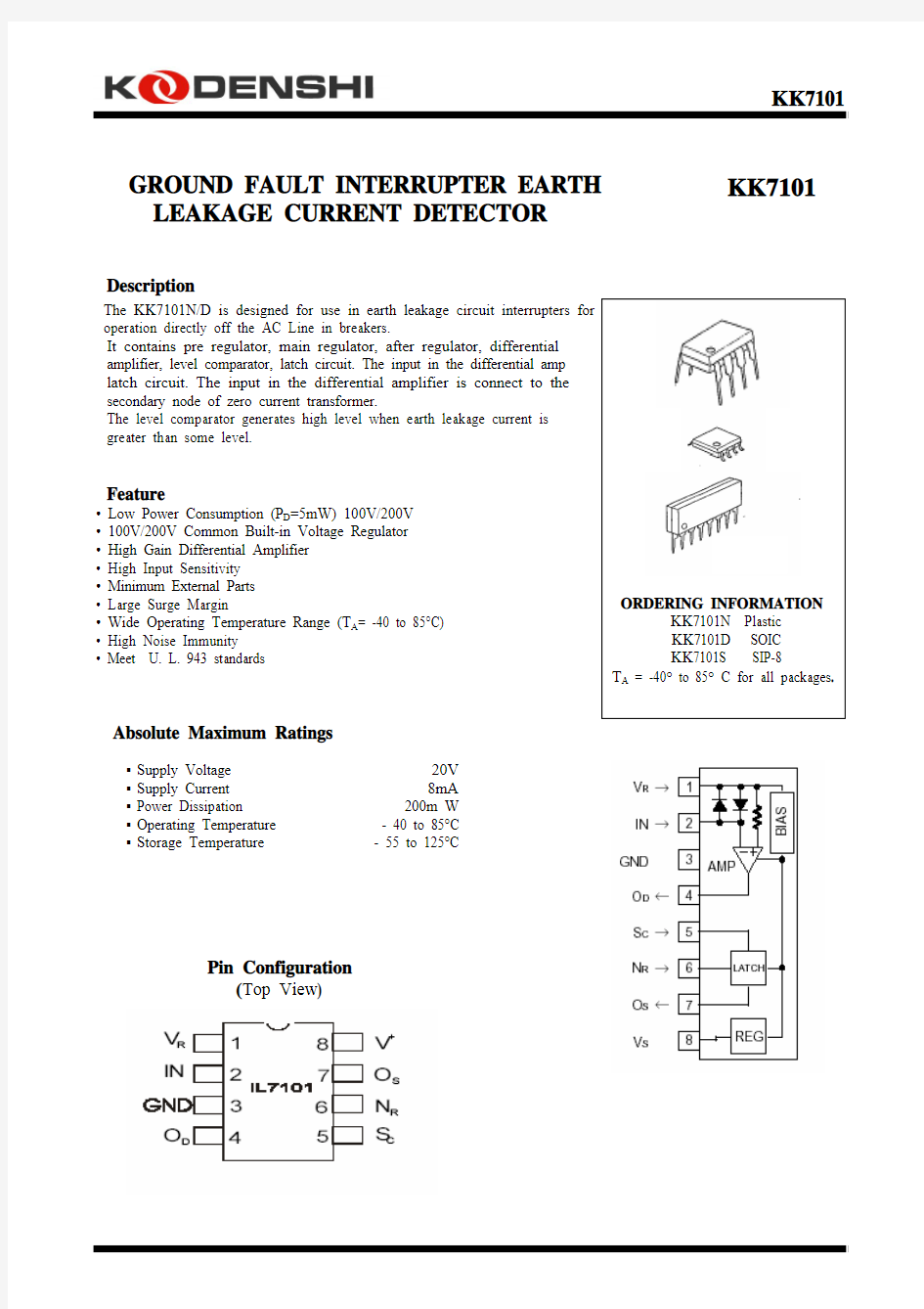
Pin Configuration (Top View )
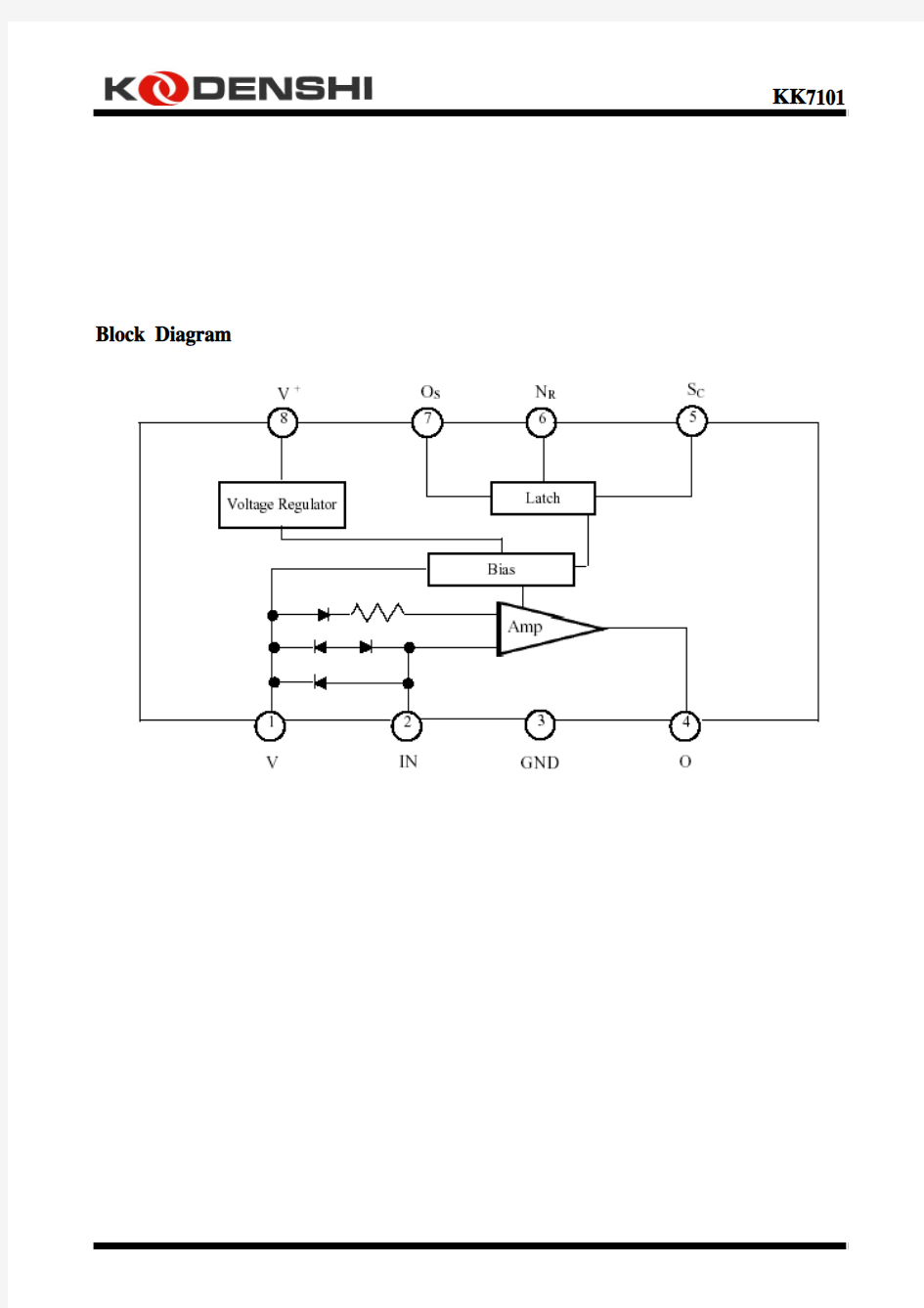
Block Diagram
Recommended Operating Condition: T A =-30°C to 80°C
PARAMETER SYMBOL MIN. TYP. MAX
UNIT Supply Voltage V + 12 V Vs-GND Capacitor Cvs 1 μF O S -GND Capacitor Cos 1 μF
Electrical Characteristics
PARAMETER
SYMBOL
CONDTIONS TEMP.(°C)
MIN. TYP. MAX. UNIT
-30 - - 580
25 - 400 530
Supply Current 1 l S1 V +=12V,
V R - V I = 30 mV
85 - - 480
μA * Trip Voltage V T V +
= 16V,
V R - V I = X
-30 85 9 13.5 18 mV (rms)Differential Amplifier
Output Current 1 I TD1 V +
= 16 V, V R - V I = 30 mV V OD = 1.2 V 25 -12 - -30 μA Differential
Amplifier Output current 2 I TD2
V + = 16 V, V R - V I = short V OD = 0.8 V
25 17 - 37 μA l SI = 580μA
-30 -200 - l SI = 530μA 25 -100 - Output Current I O V SC = 1.4 V
V OS = 0.8 V
l SI = 480μA
85 -75 - μA S C O N Voltage V SC ON V +
= 16 V
25 0.7 - 1.4 V S C Input Current I SC ON V + = l2V
25 - - 5 μA Output "L" Current I OSL V + = 12 V,
V OSL = 0.2 V
-30 85 200 - - μA Input Clamp Voltage
V IC V +
= 12 V,
I IC = 20 mA
-30 85 4.3 - 6.7 V Differential Input Clamp Voltage V IDC I IDC = 100mA -30 85 0.4 - 2 V Max. Current Voltage
V SM I SM = 7 mA
25 20 - 28 V Supply Current 2 I S2 V OS = 0.5 V, V R - V I = X
-30 85 - - 1200 μA Latch Circuit Off Supply Voltage V+ OFF 25 0.5 V Response Time
T ON
V + = 16 V, V R - V I = 0.3 V
25 1 - 4 ms
* A: 9 ~12.5 B: 11.5~15.5 C: 14.5~18
Typical Performance Curves
Typical Application
Supply voltage circuit is connected as a previous diagram. Please decide constants R1, R2, C4, and C5 of a filter in order to keep at least 12V in Vs, when normal supply current flows.
In this case, please connect C4 (more than 1?) and C2 (less than 1?). ZCT and load resistance R L of ZCT are connected between input pin① and ②. In this case protective resistance (R3=100?) must be insulted.
Sensitivity current is regulated by RL, and output of amplifier shows in pin④. External capacitor C1 between pin④ and GND is used for noise removal.
When large current is grounded in the primary side (AC line) of ZCT, the wave form in the secondary side of ZCT is distorted and some signals doesn’t appear in the output of amplifier. So please connect a varistor or
a diode (2pcs.) to ZCT in parallel.
Latch circuit is used to inspect the output level of amplifier and to supply gate current on the external SCR.
When input pin becomes more than 1.1V (Typ.) latch circuit operates and supply gate current in the gate of SCR connected to the output pin⑦.
Pin⑥ can be used in the open state, but please connect capacitor (about 0.047?) between pin⑥ and ⑦.
Capacitor C6 between pin① and GND is used to remove noise and is about 0.047?.