DS32B35-33中文资料

General Description
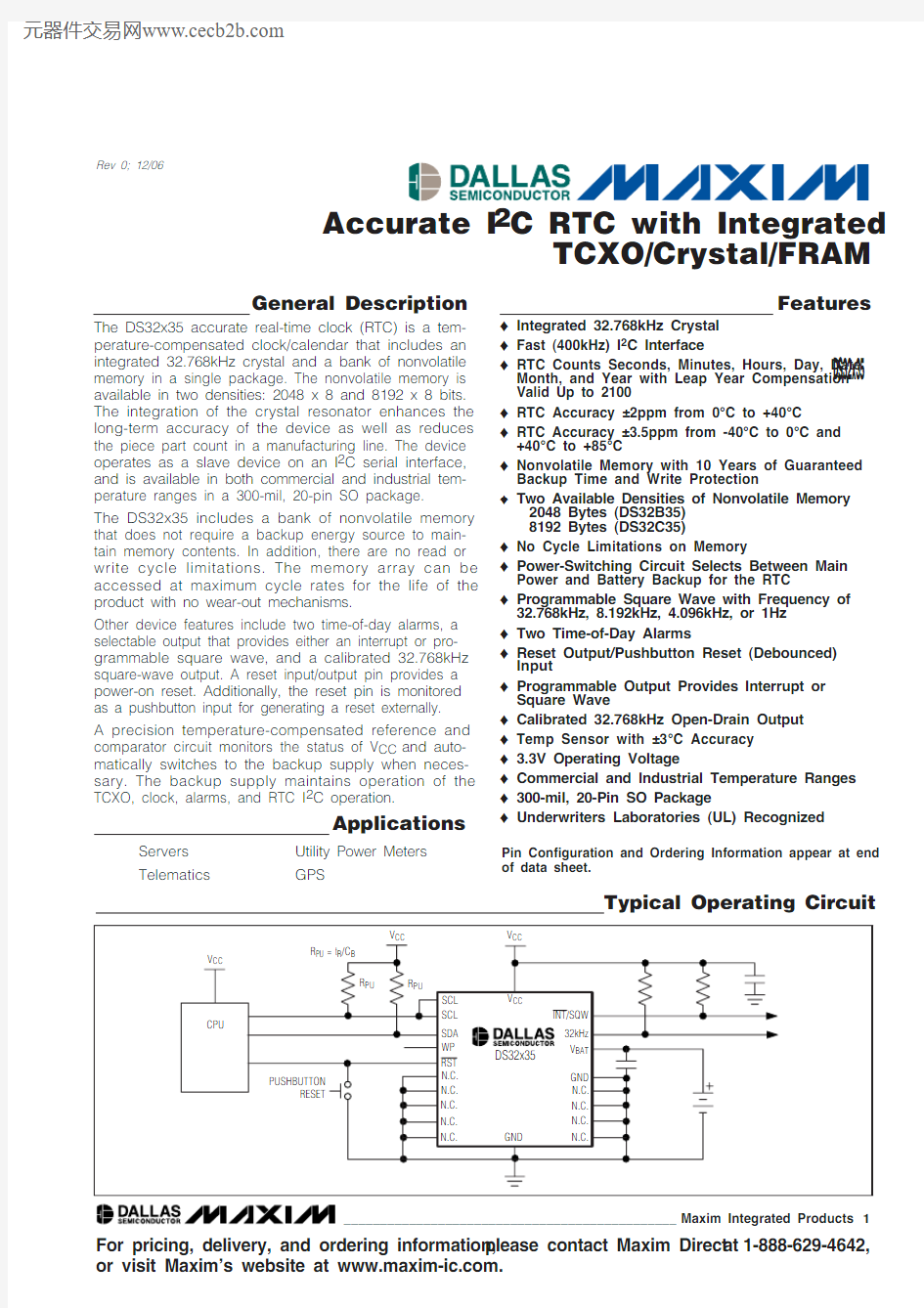
The DS32x35 accurate real-time clock (RTC) is a tem-perature-compensated clock/calendar that includes an integrated 32.768kHz crystal and a bank of nonvolatile memory in a single package. The nonvolatile memory is available in two densities: 2048 x 8 and 8192 x 8 bits.The integration of the crystal resonator enhances the long-term accuracy of the device as well as reduces the piece part count in a manufacturing line. The device operates as a slave device on an I 2C serial interface,and is available in both commercial and industrial tem-perature ranges in a 300-mil, 20-pin SO package.
The DS32x35 includes a bank of nonvolatile memory that does not require a backup energy source to main-tain memory contents. In addition, there are no read or write cycle limitations. The memory array can be accessed at maximum cycle rates for the life of the product with no wear-out mechanisms.
Other device features include two time-of-day alarms, a selectable output that provides either an interrupt or pro-grammable square wave, and a calibrated 32.768kHz square-wave output. A reset input/output pin provides a power-on reset. Additionally, the reset pin is monitored as a pushbutton input for generating a reset externally.A precision temperature-compensated reference and comparator circuit monitors the status of V CC and auto-matically switches to the backup supply when neces-sary. The backup supply maintains operation of the TCXO, clock, alarms, and RTC I 2C operation.
Applications
Servers Utility Power Meters Telematics
GPS
Features
o Integrated 32.768kHz Crystal o Fast (400kHz) I 2C Interface
o RTC Counts Seconds, Minutes, Hours, Day, Date,Month, and Year with Leap Year Compensation Valid Up to 2100
o RTC Accuracy ±2ppm from 0°C to +40°C
o RTC Accuracy ±3.5ppm from -40°C to 0°C and +40°C to +85°C
o Nonvolatile Memory with 10 Years of Guaranteed Backup Time and Write Protection
o Two Available Densities of Nonvolatile Memory
2048 Bytes (DS32B35)8192 Bytes (DS32C35)
o No Cycle Limitations on Memory
o Power-Switching Circuit Selects Between Main Power and Battery Backup for the RTC
o Programmable Square Wave with Frequency of 32.768kHz, 8.192kHz, 4.096kHz, or 1Hz o Two Time-of-Day Alarms
o Reset Output/Pushbutton Reset (Debounced)Input
o Programmable Output Provides Interrupt or Square Wave
o Calibrated 32.768kHz Open-Drain Output o Temp Sensor with ±3°C Accuracy o 3.3V Operating Voltage
o Commercial and Industrial Temperature Ranges o 300-mil, 20-Pin SO Package
o Underwriters Laboratories (UL) Recognized
DS32x35
Accurate I 2C RTC with Integrated
TCXO/Crystal/FRAM
______________________________________________Maxim Integrated Products 1
Rev 0; 12/06
For pricing, delivery, and ordering information,please contact Maxim Direct at 1-888-629-4642,or visit Maxim’s website at https://www.360docs.net/doc/c34487104.html,.
Pin Configuration and Ordering Information appear at end of data sheet.
D S 32x 35
Accurate I 2C RTC with Integrated TCXO/Crystal/FRAM 2_____________________________________________________________________
ABSOLUTE MAXIMUM RATINGS
RECOMMENDED DC OPERATING CONDITIONS
Stresses beyond those listed under “Absolute Maximum Ratings” may cause permanent damage to the device. These are stress ratings only, and functional operation of the device at these or any other conditions beyond those indicated in the operational sections of the specifications is not implied. Exposure to absolute maximum rating conditions for extended periods may affect device reliability.
Voltage Range on Any Pin Relative to Ground......-0.3V to +5.0V Operating Temperature Range ..........................-40°C to +85°C Junction Temperature......................................................+125°C Storage Temperature Range...............................-40°C to +85°C
Lead Temperature (soldering, 10s).................................+260°C Soldering Temperature....................................................See the
IPC/JEDEC J-STD-020 Specification
ELECTRICAL CHARACTERISTICS
DS32x35
Accurate I 2C RTC with Integrated
TCXO/Crystal/FRAM
_____________________________________________________________________3
ELECTRICAL CHARACTERISTICS (continued)
ELECTRICAL CHARACTERISTICS
D S 32x 35
Accurate I 2C RTC with Integrated TCXO/Crystal/FRAM 4_____________________________________________________________________
AC ELECTRICAL CHARACTERISTICS
DS32x35
Accurate I 2C RTC with Integrated
TCXO/Crystal/FRAM
_____________________________________________________________________
5
POWER-SWITCH CHARACTERISTICS
Note 1:Limits at -40°C are guaranteed by design and not production tested.Note 2:All voltages are referenced to ground.
Note 3:To minimize current drain on V BAT when the internal supply is switched to V BAT , the V IH minimum must be higher than
V BAT - 0.6V. Otherwise, there is significant current drain due to the input stage at the SCL and SDA pins.
Note 4:The pullup resistor voltage on the 32kHz and INT /SQW pins can be up to 5.5V maximum regardless of the voltage on V CC .Note 5:Current is the averaged input current, which includes the temperature conversion current.Note 6:The RST pin has an internal 50k Ω(nominal) pullup resistor to V CC .Note 7:After this period, the first clock pulse is generated.
Note 8: A device must internally provide a hold time of at least 300ns for the SDA signal (referred to as the V IH(MIN)of the SCL sig-nal) to bridge the undefined region of the falling edge of SCL.
Note 9:The maximum t HD:DAT needs only to be met if the device does not stretch the low period (t LOW ) of the SCL signal.
Note 10:A fast-mode device can be used in a standard-mode system, but the requirement t SU:DAT ≥250ns must then be met. This
is automatically the case if the device does not stretch the low period of the SCL signal. If such a device does stretch the low period of the SCL signal, it must output the next data bit to the SDA line t R(MAX)+ t SU:DAT = 1000 + 250 = 1250ns before the SCL line is released.
Note 11:C B —total capacitance of one bus line in pF.
Note 12:The parameter t OSF is the period of time the oscillator must be stopped for the OSF flag to be set over the voltage range of
0.0V ≤V CC ≤V CC(MAX) and 2.0V ≤V BAT ≤3.6V.
Note 13:This delay applies only if the oscillator is enabled and running. If the EOSC bit is a 1, t REC is bypassed and RST immediate-ly goes high.
D S 32x 35
Accurate I 2C RTC with Integrated TCXO/Crystal/FRAM 6_____________________________________________________________________
Pushbutton Reset Timing
Power-Switch Timing
DS32x35
Accurate I 2C RTC with Integrated
TCXO/Crystal/FRAM
_____________________________________________________________________7
SUPPLY CURRENT vs. TEMPERATURE
TEMPERATURE (°C)I B A T (μA )
80.0
60.040.020.00.0-20.0
0.700
0.800
0.9001.000
0.600
-40.0FREQUENCY DEVIATION vs.TEMPERATURE vs. AGING VALUE
CRYSTAL AGING REGISTER VALUE
F R E Q U E N C Y D E V I A T I O N (p p m )
96
64
32
-64
-32
-96
-40
-30-20-100102030405060-128128
STANDBY SUPPLY CURRENT vs. SUPPLY VOLTAGE
V CC (V)
I C C S (μA )
5.0
4.03.0
50
100150
02.0
SUPPLY CURRENT vs. SUPPLY VOLTAGE
V BAT (V)
I B A T (μA )
5.0
4.03.0
0.800
0.900
1.000
1.100
1.200
0.700
2.0
Typical Operating Characteristics
(V CC = +3.3V, T A = +25°C, unless otherwise noted.)
D S 32x 35
Accurate I 2C RTC with Integrated TCXO/Crystal/FRAM 8_____________________________________________________________________
Block Diagram
DS32x35
Accurate I 2C RTC with Integrated
TCXO/Crystal/FRAM
_____________________________________________________________________
9
Detailed Description
The DS32x35 accurate RTC is a temperature-compen-sated clock/calendar that includes an integrated 32.768kHz crystal and a bank of nonvolatile memory in a single package. The nonvolatile memory is available in two sizes: 2048 x 8 or 8192 x 8 bits. The integration of the crystal resonator enhances the long-term accura-cy of the device as well as reduces the piece part count in a manufacturing line. The device is available in both commercial and industrial temperature ranges and is offered in a 300-mil, 20-pin SO package.
The DS32x35 includes a bank of nonvolatile memory that does not require a backup energy source to main-tain the memory contents. In addition, there are no read
accessed at maximum cycle rates for the life of the product with no wear-out mechanisms.
A precision temperature-compensated reference and comparator circuit monitors the status of V CC and auto-matically switches to the backup supply when neces-sary. Other device features include two time-of-day alarms, a selectable output that provides either an interrupt or programmable square wave, and a calibrat-ed 32.768kHz square-wave output. A reset input/output pin provides a power-on reset. Additionally, the reset pin is monitored as a pushbutton input for generating a reset externally. The device is accessed through an I 2C serial interface.
D S 32x 35
Accurate I 2C RTC with Integrated TCXO/Crystal/FRAM 10
____________________________________________________________________
Operation
The Block Diagram shows the main elements of the DS32x35. The nine blocks can be grouped into six functional groups: TCXO, power control, pushbutton function, RTC, I 2C interface, and F RAM. Their opera-tions are described separately in the following sections.
32kHz TCXO
The temperature sensor, oscillator, and control logic form the TCXO. The controller reads the output of the on-chip temperature sensor and uses a lookup table to determine the capacitance required, adds the aging correction in the AGE register, and then sets the capacitance selection registers. New values, including changes to the AGE register, are loaded only when a change in the temperature value occurs, or when a user-initiated temperature conversion is completed.The temperature is read on initial application of V CC and once every 64 seconds afterwards while the device is powered by either V CC or V BAT .
Power Control
This function is provided by a temperature-compensat-ed voltage reference and a comparator circuit that monitors the V CC level. When V CC is greater than V PF ,the part is powered by V CC . When V CC is less than V PF but greater than V BAT , the RTC is powered by V CC . If V CC is less than V PF and is less than V BAT , the device is powered by V BAT . See Table 1.
The RTC can be accessed when the device is powered by either V CC or V BAT . The F RAM is only accessible when the device is powered by V CC . The F RAM must not be accessed when V CC < V CC(MIN).
To preserve the battery, the first time V BAT is applied to the device, the oscillator will not start up until V CC exceeds V PF , or until a valid I 2C address is written to the part. Typical oscillator startup time is less than one sec-ond. Approximately 2 seconds after V CC is applied, or a valid I 2C address is written, the device makes a temper-ature measurement and applies the calculated correc-tion to the oscillator. Once the oscillator is running, it
continues to run as long as a valid power source is avail-able (V CC or V BAT ), and the device continues to mea-sure the temperature and correct the oscillator frequency every 64 seconds.
Pushbutton Reset Function
The DS32x35 provides for a pushbutton switch to be con-nected to the RST output pin. When the device is not in a reset cycle, it continuously monitors the RST signal for a low going edge. If an edge transition is detected, the device debounces the switch by pulling RST low. After the internal timer has expired (PB DB ), the device contin-ues to monitor the RST line. If the line is still low, the device continuously monitors the line looking for a rising edge. Upon detecting release, the device forces the RST pin low and holds it low for t RST .
RST is also used to indicate a power-fail condition.When V CC is lower than V PF , an internal power-fail sig-nal is generated, which forces the RST pin low. When V CC returns to a level above V PF , the RST pin is held low for t REC to allow the power supply to stabilize. If the oscillator is not running (see the Power Control section)when V CC is applied, t REC is bypassed and RST imme-diately goes high. The state of RST does not affect the operation of the TCXO, I 2C interface, F RAM, or RTC functions.
Real-Time Clock
With the clock source from the TCXO, the RTC provides seconds, minutes, hours, day, date, month, and year information. The date at the end of the month is automati-cally adjusted for months with fewer than 31 days, includ-ing corrections for leap year. The clock operates in either the 24-hour or 12-hour format with an AM /PM indicator.
The clock provides two programmable time-of-day
alarms and a programmable square-wave output. The
INT /SQW pin either generates an interrupt due to alarm
condition or outputs a square-wave signal and the
selection is controlled by the bit INTCN.
I 2C Interface
The FRAM I 2C interface is accessible whenever V
CC is
at a valid level. The RTC I 2C interface is accessible
whenever either V CC or V BAT is at a valid level. If a microcontroller connected to the device resets because
of a loss of V CC or other event, it is possible that the microcontroller and the RTC I 2C communications could become unsynchronized, e.g., the microcontroller resets while reading data from the RTC. When the microcon-troller resets, the RTC I 2C interface may be placed into a known state by toggling SCL until SDA is observed to be at a high level. At that point the microcontroller should pull SDA low while SCL is high, generating a START condition.
DS32x35
Accurate I 2C RTC with Integrated
TCXO/Crystal/FRAM
____________________________________________________________________11
FRAM
The serial F RAM memory is logically organized as a 2048 x 8 or 8192 x 8 memory array and is accessed using the I 2C interface. F unctional operation of the F RAM is similar to serial EEPROMs with the major dif-ference being its superior performance on writes. The memory is read or written at the speed of the I 2C inter-face. It is not necessary to poll the device for a ready condition during writes.
Due to the different memory densities, the I 2C address-ing technique is different for each version of the DS32x35. See the I 2C Serial Data Bus section for details.
Warning:The F RAM does not inhibit reads or writes
when V CC is below the minimum operating voltage.F RAM reads are destructive, that is, when a read is performed, the device internally writes the memory back to the original value. The FRAM must not be read or written when V CC is below the minimum operating voltage; otherwise, the memory cells may not be fully programmed, and the data may not be retained.
RTC Address Map
Table 3 shows the RTC address map for the DS32x35timekeeping registers. During a multibyte access, when the address pointer reaches the end of the register space, it wraps around to location 00h. On an I 2C START or address pointer incrementing to location 00h,the current time is transferred to a second set of regis-ters. The time information is read from these secondary registers, while the clock continues to run. This elimi-nates the need to reread the registers in case the main registers update during a read.
Clock and Calendar
The time and calendar information is obtained by read-ing the appropriate register bytes. Table 3 illustrates the RTC registers. The time and calendar data are set or ini-tialized by writing the appropriate register bytes. The con-tents of the time and calendar registers are in the binary-coded decimal (BCD) format. The DS32x35 can be run in either 12-hour or 24-hour mode. Bit 6 of the hours register is defined as the 12- or 24-hour mode select bit. When high, the 12-hour mode is selected. In the 12-hour mode, bit 5 is the AM /PM bit with logic-high being PM. In the 24-hour mode, bit 5 is the second 10-hour bit (20 to 23 hours). The century bit (bit 7 of the month register) is toggled when the years register over-flows from 99 to 00.
The day-of-week register increments at midnight.Values that correspond to the day of week are user-defined but must be sequential (i.e., if 1 equals Sunday, then 2 equals Monday, and so on). Illogical time and date entries result in undefined operation.
When reading or writing the time and date registers, sec-ondary (user) buffers are used to prevent errors when the internal registers update. When reading the time and date registers, the user buffers are synchronized to the internal registers on any START and when the register pointer rolls over to zero. The time information is read from these secondary registers while the clock continues to run. This eliminates the need to reread the registers in case the main registers update during a read.
The countdown chain is reset whenever the seconds register is written. Write transfers occur on the acknowl-edge from the DS32x35. Once the countdown chain is reset, to avoid rollover issues the remaining time and date registers must be written within 1 second. The 1Hz square-wave output, if enabled, transitions high 500ms after the seconds data transfer, provided that the oscil-lator is already running.
D S 32x 35
Accurate I 2C RTC with Integrated TCXO/Crystal/FRAM 12____________________________________________________________________
Table 3. RTC Register Map
DS32x35
Alarms
The DS32x35 contains two time-of-day/date alarms.Alarm 1 can be set by writing to registers 07h to 0Ah.Alarm 2 can be set by writing to registers 0Bh to 0Dh.The alarms can be programmed (by the alarm enable and INTCN bits of the Control register) to activate the INT /SQW output on an alarm match condition. Bit 7 of each of the time-of-day/date alarm registers are mask bits (Table 4). When all the mask bits for each alarm are logic 0, an alarm only occurs when the values in the timekeeping registers match the corresponding values stored in the time-of-day/date alarm registers. The alarms can also be programmed to repeat every sec-ond, minute, hour, day, or date. Table 4 shows the
possible settings. Configurations not listed in the table will result in illogical operation.
The DY/DT bits (bit 6 of the alarm day/date registers)control whether the alarm value stored in bits 0 to 5 of that register reflects the day of the week or the date of the month. If DY/DT is written to logic 0, the alarm is the result of a match with date of the month. If DY/DT is written to logic 1, the alarm is the result of a match with day of the week.
When the RTC register values match alarm register set-tings, the corresponding Alarm Flag (“A1F”) or (“A2F”)bit is set to logic 1. If the corresponding alarm interrupt enable (“A1IE”) or (“A2IE”) is also set to logic 1 and the INTCN bit is set to logic 1, the alarm condition will acti-vate the INT /SQW signal.
Accurate I 2C RTC with Integrated
TCXO/Crystal/FRAM
____________________________________________________________________13
D S 32x 35
Accurate I 2C RTC with Integrated TCXO/Crystal/FRAM 14____________________________________________________________________
Special-Purpose Registers
Control Register (0Eh)
Bit 7: Enable Oscillator (EOSC ). When set to logic 0,the oscillator is started. When set to logic 1, the oscilla-tor is stopped when the DS32x35 switches to V BAT .This bit is clear (logic 0) when power is first applied.When the DS32x35 is powered by V CC , the oscillator is always on regardless of the status of the EOSC bit.
Bit 6: Battery-Backed Square-Wave Enable (BBSQW). When set to logic 1 and the DS32x35is being powered by the V BAT pin, this bit enables the square-wave or interrupt output when V CC is absent.When BBSQW is logic 0, the INT /SQW pin goes high impedance when V CC falls below the power-fail trip point. This bit is disabled (logic 0) when power is first applied.
Bit 5: Convert Temperature (CON V). When the DS32x35 is in idle state, setting this bit to 1 forces the temperature sensor to convert the temperature into dig-ital code and execute the TCXO algorithm to update the capacitance load for the oscillator. This can only happen when a conversion is not already in progress.The user should check the status bit BSY before forcing the controller to start a new TCXO execution. A user-ini-tiated temperature conversion does not affect the inter-nal 64-second update cycle.
Bits 4 and 3: Rate Select (RS2 and RS1). These bits control the frequency of the square-wave output when the square wave has been enabled. Table 5 shows the square-wave frequencies that can be selected with the RS bits. These bits are both set to logic 1 (8.192kHz)when power is first applied.
Bit 2: Interrupt Control (INTCN). This bit controls the INT /SQW signal. When the INTCN bit is set to logic 0, a square wave is output on the INT /SQW pin. When the INTCN bit is set to logic 1, then a match between the timekeeping registers and either of the alarm registers activates the INT /SQW output (if the alarm is also enabled). The corresponding alarm flag is always set regardless of the state of the INTCN bit. The INTCN bit is set to logic 1 when power is first applied.
Bit 1: Alarm 2 Interrupt Enable (A2IE).When set to logic 1, this bit permits the alarm 2 flag (A2F) bit in the status register to assert INT /SQW (when INTCN = 1).When the A2IE bit is set to logic 0 or INTCN is set to logic 0, the A2F bit does not initiate an interrupt signal.The A2IE bit is disabled (logic 0) when power is first applied.
Bit 0: Alarm 1 Interrupt Enable (A1IE).When set to logic 1, this bit permits the alarm 1 flag (A1F) bit in the status register to assert INT /SQW (when INTCN = 1).When the A1IE bit is set to logic 0 or INTCN is set to logic 0, the A1F bit does not initiate the INT /SQW sig-nal. The A1IE bit is disabled (logic 0) when power is first applied.
DS32x35
Accurate I 2C RTC with Integrated
TCXO/Crystal/FRAM
____________________________________________________________________15
Bit 7: Oscillator Stop Flag (OSF). A logic 1 in this bit indicates that the oscillator either is stopped or was stopped for some period and may be used to judge the validity of the timekeeping data. This bit is set to logic 1any time that the oscillator stops. The following are examples of conditions that can cause the OSF bit to be set:
1)The first time power is applied.
2)The voltages present on both V CC and V BAT are insufficient to support oscillation.
3)The EOSC bit is turned off in battery-backed mode.4)External influences on the crystal (i.e., noise, leak-age, etc.).
This bit remains at logic 1 until written to logic 0.
Bit 3: Enable 32kHz Output (EN32kHz).This bit con-trols the status of the 32kHz pin. When set to logic 1,the 32kHz pin is enabled and outputs a 32.768kHz square-wave signal. When set to logic 0, the 32kHz pin goes to a high-impedance state. The initial power-up state of this bit is logic 1, and a 32.768kHz square-wave signal appears at the 32kHz pin after a V CC is applied to the DS32x35.
Bit 2: Busy (BSY).This bit indicates the device is busy executing TCXO functions. It goes to logic 1 when the conversion signal to the temperature sensor is asserted and then is cleared when the device is in the 1-minute
CONV signal from aborting the execution of the TCXO algorithm and starting a new execution of TCXO function.Bit 1: Alarm 2 Flag (A2F).A logic 1 in the alarm 2 flag bit indicates that the time matched the alarm 2 regis-ters. If the A2IE bit is logic 1 and the INTCN bit is set to logic 1, the INT /SQW pin is also asserted. A2F is cleared when written to logic 0. This bit can only be written to logic 0. Attempting to write to logic 1 leaves the value unchanged.
Bit 0: Alarm 1 Flag (A1F).A logic 1 in the alarm 1 flag bit indicates that the time matched the alarm 1 regis-ters. If the A1IE bit is logic 1 and the INTCN bit is set to logic 1, the INT /SQW pin is also asserted. A1F is cleared when written to logic 0. This bit can only be written to logic 0. Attempting to write to logic 1 leaves the value unchanged.
Aging Offset Register (10h)
The Aging Offset register provides an 8-bit code to add to the codes in the capacitance array registers. The code is encoded in two’s complement. One LSB repre-sents one small capacitor to be switched in or out of the capacitance array at the crystal pins.
The change in ppm per LSB is different at different temper-atures. The frequency vs. temperature curve is distorted by the values used in this register. At +23°C, one LSB typi-cally provides approximately 0.1ppm change in frequency.
D S 32x 35
Accurate I 2C RTC with Integrated TCXO/Crystal/FRAM 16____________________________________________________________________
Temperature Registers (11h–12h)
Temperature is represented as a 10-bit code with a res-olution of +0.25°C and is accessible at location 11h and 12h. The temperature is encoded in two’s comple-ment format. The upper 8 bits are at location 11h, and the lower 2 bits are in the upper nibble at location 12h.Upon power reset, the registers are set to a default
temperature of 0°C and the controller starts a tempera-ture conversion. New temperature readings are stored in this register.
FRAM Address Map
During a multibyte access, the address pointer wraps around to location 00h when it reaches the end of the register space.
DS32x35
Accurate I 2C RTC with Integrated
TCXO/Crystal/FRAM
____________________________________________________________________
17
I 2C Serial Data Bus
The DS32x35 supports a bidirectional I 2C bus and data transmission protocol (F igure 1). A device that sends data onto the bus is defined as a transmitter, and a device receiving data is defined as a receiver. The device that controls the message is called a master.The devices that are controlled by the master are slaves. The bus must be controlled by a master device that generates the serial clock (SCL), controls the bus access, and generates the START and STOP condi-tions. The DS32x35 operates as a slave on the I 2C bus.Connections to the bus are made through the SCL
input and open-drain SDA I/O lines. Within the bus specifications, a standard mode (100kHz maximum clock rate) and a fast mode (400kHz maximum clock rate) are defined. The DS32x35 works in both modes.The following bus protocol has been defined (Figure 2):?Data transfer can be initiated only when the bus is not busy.
?During data transfer, the data line must remain stable whenever the clock line is high. Changes in the data line while the clock line is high are interpreted as control signals.
Figure 2. I C Data Transfer Overview
Figure 1. Data Transfer on I C Serial Bus
D S 32x 35
Accurate I 2C RTC with Integrated TCXO/Crystal/FRAM 18____________________________________________________________________
Accordingly, the following bus conditions have been defined:
Bus not busy:Both data and clock lines remain high.
Start data transfer:A change in the state of the data line from high to low, while the clock line is high,defines a START condition.
Stop data transfer:A change in the state of the data line from low to high, while the clock line is high,defines a STOP condition.
Data valid:The state of the data line represents valid data when, after a START condition, the data line is stable for the duration of the high period of the clock signal. The data on the line must be changed during the low period of the clock signal. There is one clock pulse per bit of data.
Each data transfer is initiated with a START condition and terminated with a STOP condition. The number of data bytes transferred between the START and the STOP conditions is not limited, and is determined by the master device. The information is transferred byte-wise and each receiver acknowledges with a ninth bit.
Acknowledge:Each receiving device, when addressed, is obliged to generate an acknowledge after the reception of each byte. The master device must generate an extra clock pulse, which is associ-ated with this acknowledge bit.
A device that acknowledges must pull down the SDA line during the acknowledge clock pulse in such a way that the SDA line is stable low during the high period of the acknowledge-related clock pulse. Of course, setup and hold times must be taken into account. A master must signal an end of data to the slave by not generating an acknowledge bit on the last byte that has been clocked out of the slave. In this case, the slave must leave the data line high to enable the master to generate the STOP condition.Depending upon the state of the R/W bit, two types of data transfer are possible:
1)Data transfer from a master transmitter to a slave receiver. The first byte transmitted by the master is the slave address. Next follows a num-ber of data bytes. The slave returns an acknowl-edge bit after each received byte. Data is transferred with the most significant bit (MSB) first.
2)Data transfer from a slave transmitter to a master receiver. The first byte (the slave address) is transmitted by the master. The slave then returns an acknowledge bit. Next follows a number of data bytes transmitted by the slave to the master. The master returns an acknowledge bit after all received bytes other than the last byte.At the end of the last received byte, a not acknowledge is returned.The master device generates all the serial clock pulses and the START and STOP conditions. A transfer is ended with a STOP condition or with a repeated START condition. Since a repeated START condition is also the beginning of the next serial transfer, the bus will not be released. Data is transferred with the most significant bit (MSB)first.
The DS32x35 can operate in the following two modes:1)Slave receiver mode (DS32x35 write mode):Serial data and clock are received through SDA and SCL.After each byte is received an acknowledge bit is transmitted. START and STOP conditions are recog-nized as the beginning and end of a serial transfer.Address recognition is performed by hardware after reception of the slave address and direction bit (see F igures 3, 5, and 7). The slave address byte is the first byte received after the master generates the START condition. The slave address byte contains one of the 7-bit DS32x35 addresses. The slave address is 1101000 for the RTC. F or the DS32B35FRAM, the first four bits are 1010, and the next three bits select one of eight blocks of data (see Table 2).F or the DS32C35 F RAM, the first seven bits are 1010000. Each slave address is followed by the direction bit (R/W ), which is zero for a write. After receiving and decoding the slave address byte, the device outputs an acknowledge on the SDA line.After the device acknowledges the slave address and write bit, the master transmits a register address to the device. For the DS32C35, the master transmits two bytes for the register address information. This sets the register pointer on the device. After setting the register address, the master then transmits zero or more bytes of data with the DS32x35 acknowl-edging each byte received. The master generates a STOP condition to terminate the data write.
2)Slave transmitter mode (DS32x35 read mode):The first byte is received and handled as in the slave receiver mode. However, in this mode, the direction bit indicates that the transfer direction is reversed.The DS32x35 transmits serial data on SDA while the serial clock is input on SCL. START and STOP con-ditions are recognized as the beginning and end of a serial transfer (see F igure 4). The slave address byte is the first byte received after the master gener-ates the START condition. The slave address byte contains one of the 7-bit DS32x35 addresses. The slave address is 1101000 for the RTC. F or the DS32B35 FRAM, the first four bits are 1010, and the next three bits select one of eight blocks of data
(see Table 2). Each slave address is followed by the direction bit (R/W ), which is one for a read. After receiving and decoding the slave address byte, the device outputs an acknowledge on the SDA line.The DS32x35 then begins to transmit data starting with the register address pointed to by the register pointer. If the register pointer is not written to before the initiation of a read mode, the first address that is read is the last one stored in the register pointer. The DS32x35 must receive a "not acknowledge" to end a read. The register pointer can be set prior to a data read by initiating a slave receiver mode sequence,with no data bytes transmitted after the register address data.
DS32x35
Accurate I 2C RTC with Integrated
TCXO/Crystal/FRAM
____________________________________________________________________19
Figure 3. Data Write—RTC Slave Receiver Mode
Figure 4. Data Read—RTC Slave Transmitter Mode
Figure 5. Data Write—DS32B35 FRAM Slave Receiver Mode
D S 32x 35
Accurate I 2C RTC with Integrated TCXO/Crystal/FRAM 20____________________________________________________________________
Figure 6. Data Read—DS32B35 FRAM Slave Transmitter Mode
Figure 7. Data Write—DS32C35 FRAM Slave Receiver Mode
Figure 8. Data Read—DS32C35 FRAM Slave Transmitter Mode
Handling, PCB Layout, and
Assembly
The DS32x35 package contains a quartz tuning-fork crystal. Pick-and-place equipment can be used, but precautions should be taken to ensure that excessive shocks are avoided. Ultrasonic cleaning should be avoided to prevent damage to the crystal.
Avoid running signal traces under the package, unless a ground plane is placed between the package and the signal line. All N.C. (no connection) pins must be connected to ground.
Moisture-sensitive packages are shipped from the fac-tory dry packed. Handling instructions listed on the package label must be followed to prevent damage during reflow. See IPC/JEDEC J-STD-020 standard for moisture-sensitive device (MSD) classifications and reflow profiles.