PL611S-02-XXXGCR中文资料

元器件交易网https://www.360docs.net/doc/c34779455.html,
(Preliminary)
PL611s-02
1.8V-3.3V PicoPLL TM , World’s Smallest Programmable Clock
FEATURES
? Lowest-power, smallest Programmable PLL ? Very low Jitter and Phase Noise ? Output Frequency up to: o 133MHz @ 1.8V operation o 166MHz @ 2.5V operation o 200MHz @ 3.3V operation ? Input Frequency: o Fundamental Crystal: 10MHz to 50MHz o Reference Clock: 1MHz to 200MHz ? Accepts >0.1V reference signal input voltage ? One I/O pin can be configured as Output Enable (OE), Frequency switching (FSEL), Power Down (PDB) input, or CLK1 output. ? <10 A current consumption with PDB active. ? Single 1.8V, 2.5V, or 3.3V ± 10% power supply ? Operating temperature range from -40°C to 85°C ? Available in 6-pin DFN, SOT23, and SC70 GREEN/RoHS compliant packages.
DESCRIPTION
The PL611s-02 is a low-power, small form factor, high performance OTP-base programmable frequency synthesizer and a member of PhaseLink’s PicoPLL Factory Programmable ‘Quick Turn Clocks. Designed to fit in a small DFN, SC70, or SOT23 package for a broad range of applications, the PL611s-02 offers the best phase noise and jitter performance, and power consumption of its rivals. . In addition, one programmable I/O pin can be configured as Output Enable (OE), Frequency switching (FSEL), Power Down (PDB) input, or CLK1 (F OUT , F REF , F REF /2) output. The power down feature of PL611s-02, when activated, allows the IC to consume less than 10 A of power, while its programming flexibility allows generating any output, up to 200MHz using a low-cost crystal or reference input.
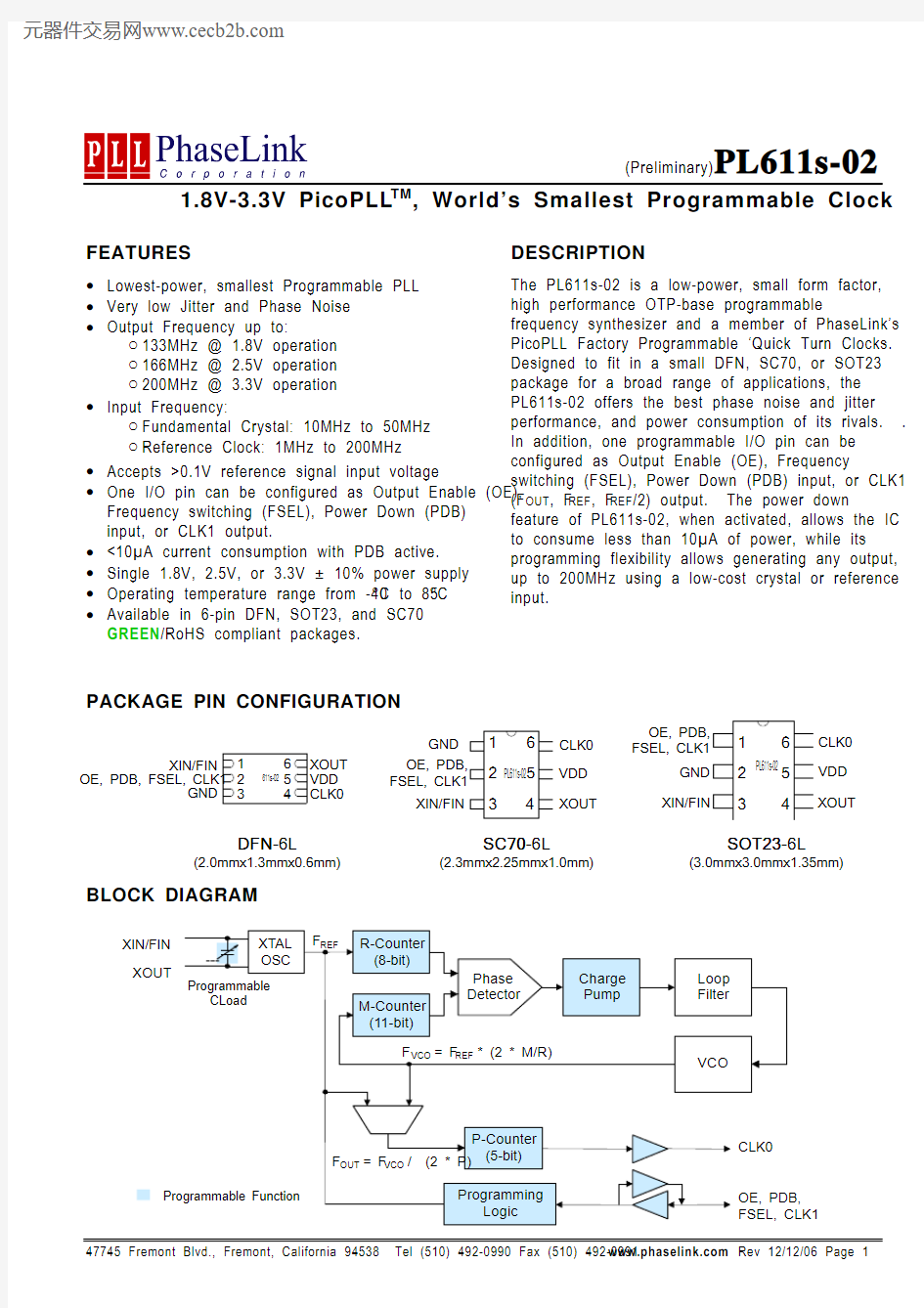
PACKAGE PIN CONFIGURATION
GND XIN/FIN OE, PDB, FSEL, CLK1 GND 1 2 3 6 5 4 XOUT VDD CLK0
611s-02
1 2 3
6 5 4
CLK0 VDD XOUT
OE, PDB, FSEL, CLK1 GND XIN/FIN
PL611s-02
1 2 3
6 5 4
CLK0 VDD XOUT
PL611s-02
OE, PDB, FSEL, CLK1 XIN/FIN
DFNDFN-6L
(2.0mmx1.3mmx0.6mm)
SC70SC70-6L 70
(2.3mmx2.25mmx1.0mm)
SOT23SOT23-6L 23
(3.0mmx3.0mmx1.35mm)
BLOCK DIAGRAM
XIN/FIN XOUT XTAL OSC
Programmable CLoad
FREF
R-Counter (8-bit) M-Counter (11-bit) Phase Detector Charge Pump Loop Filter
F VCO = F REF * (2 * M/R)
VCO
P-Counter (5-bit) FOUT = F VCO / (2 * P)
Programmable Function
CLK0
Programming Logic
OE, PDB, FSEL, CLK1
47745 Fremont Blvd., Fremont, California 94538 Tel (510) 492-0990 Fax (510) 492-0991 https://www.360docs.net/doc/c34779455.html, Rev 12/12/06 Page 1
元器件交易网https://www.360docs.net/doc/c34779455.html,
(Preliminary)
PL611s-02
1.8V-3.3V PicoPLL TM , World’s Smallest Programmable Clock
KEY PROGRAMMING PARAMETERS
CLK Output Frequency FOUT = FREF * M / (R * P) Where M = 11 bit R = 8 bit P = 5 bit CLK0 = FOUT, FREF or FREF / (2*P) CLK1 = FREF, FREF/2, CLK0 or CLK0/2 Output Drive Strength Three optional drive strengths to choose from: ? Low: 4mA ? Std: 8mA (default) ? High: 16mA Programmable Input/Output One output pin can be configured as: ? OE - input ? PDB - input ? FSEL - input ? CLK1 – output
PACKAGE PIN ASSIGNMENT
Pin Assignment Name
SOT23 Pin # SC70 Pin# DFN Pin#
Type
Description This programmable I/O pin can be configured as an Output Enable (OE) input, Power Down input (PDB), On-the-Fly Frequency Switching Selector (FSEL), or CLK1 clock output This pin has an internal 60K pull up resistor for OE, PDB & FSEL.
State 0 1 (default) OE Tri-State CLK Normal mode PDB Power Down Mode Normal mode FSEL Frequency ‘2’ Frequency ‘1’
OE, PDB, FSEL, CLK1
1
2
2
I/O
GND XIN, FIN XOUT VDD CLK0
2 3 4 5 6
1 3 4 5 6
3 1 6 5 4
P I O
GND connection Crystal or Reference Clock input pin Crystal Output pin Do Not Connect (DNC ) when FIN is present
P O
VDD connection Programmable Clock Output
47745 Fremont Blvd., Fremont, California 94538 Tel (510) 492-0990 Fax (510) 492-0991 https://www.360docs.net/doc/c34779455.html, Rev 12/12/06 Page 2
元器件交易网https://www.360docs.net/doc/c34779455.html,
(Preliminary)
PL611s-02
1.8V-3.3V PicoPLL TM , World’s Smallest Programmable Clock
FUNCTIONAL DESCRIPTION
PL611s-02 is a highly featured, very flexible, advanced programmable PLL design for high performance, lowpower, small form-factor applications. The PL611s-02 accepts a fundamental input crystal of 10MHz to 50MHz or reference clock input of 1MHz to 200MHz and is capable of producing two outputs up to 200MHz. This flexible design allows the PL611s-02 to deliver any PLL generated frequency, F REF (Crystal or Ref Clk) frequency or F REF /(2*P) to CLK0 and/or CLK1. Some of the design features of the PL611s-02 are mentioned below: PLL Programming The PLL in the PL611s-02 is fully programmable. The PLL is equipped with an 8-bit input frequency divider (R-Counter), and an 11-bit VCO frequency feedback loop divider (M-Counter). The output of the PLL is transferred to a 5-bit post VCO divider (PCounter). The output frequency is determined by the following formula [F OUT = F REF * M / (R * P) ]. Clock Output (CLK0) CLK0 is the main clock output. The output of CLK0 can be configured as the PLL output (F VCO /(2*P)), F REF (Crystal or Ref Clk) output, or F REF /(2*P) output. The output drive level can be programmed to Low Drive (4mA), Standard Drive (8mA) or High Drive (16mA). The maximum output frequency is determined by the Power Supply Voltage; 200MHz at 3.3V, 166MHz at 2.5V and 133MHz at 1.8V. Clock Output (CLK1) The CLK1 feature allows the PL611s-02 to have an additional clock output programmed to one of the following: F REF - Reference (Crystal or Ref Clk) Frequency F REF / 2 CLK0 CLK0 / 2 Output Enable (OE) The Output Enable feature allows the user to enable and disable the clock output(s) by toggling the OE pin. The OE pin incorporates a 60k pull up resistor giving a default condition of logic “1”. Power-Down Control (PDB) The Power Down (PDB) feature allows the user to put the PL611s-02 into “Sleep Mode”. When activated (logic ‘0’), PDB ‘Disables the PLL, the oscillator circuitry, counters, and all other active circuitry. In Power Down mode the IC consumes <10 A of power. The PDB pin incorporates a 60k pull up resistor giving a default condition of logic “1”. Frequency Select (FSEL) The Frequency Select (FSEL) feature allows the PL611s-02 to switch between two pre-programmed outputs allowing the device “On the Fly” frequency switching. The FSEL pin incorporates a 60k pull up resistor giving a default condition of logic “1”.
47745 Fremont Blvd., Fremont, California 94538 Tel (510) 492-0990 Fax (510) 492-0991 https://www.360docs.net/doc/c34779455.html, Rev 12/12/06 Page 3
元器件交易网https://www.360docs.net/doc/c34779455.html,
(Preliminary)
PL611s-02
1.8V-3.3V PicoPLL TM , World’s Smallest Programmable Clock
ELECTRICAL SPECIFICATIONS
ABSOLUTE MAXIMUM RATINGS PARAMETERS
Supply Voltage Range Input Voltage Range Output Voltage Range Soldering Temperature (Green package) Data Retention @ 85°C Storage Temperature Ambient Operating Temperature*
SYMBOL
V DD VI VO
MIN.
MAX.
7 V DD + 0.5 V DD + 0.5 260 150 85
UNITS
V V V °C Year °C °C
- 0.5 - 0.5 - 0.5
10
TS
-65 -40
Exposure of the device under conditions beyond the limits specified by Maximum Ratings for extended periods may cause permanent damage to the device and affect product reliability. These conditions represent a stress rating only, and functional operations of the device at these or any other conditions above the operational limits noted in this specification is not implied. *Operating temperature is guaranteed by design. Parts are tested to commercial grade only.
AC SPECIFICATIONS
PARAMETERS
Crystal Input Frequency (XIN) Input (FIN) Frequency Input (FIN) Signal Amplitude Input (FIN) Signal Amplitude Output Frequency Settling Time Output Enable Time VDD Sensitivity Output Rise Time Output Fall Time
CONDITIONS
Fundamental Crystal @ V DD =3.3V @ V DD =2.5V @ V DD =1.8V Internally AC coupled (High Frequency) Internally AC coupled (Low Frequency) 3.3V <50MHz, 2.5V <40MHz, 1.8V <15MHz @ VDD =3.3V @ VDD =2.5V @ VDD =1.8V At power-up (after VDD increases over 1.62V) OE Function; Ta=25o C, 15pF Load PDB Function; Ta=25o C, 15pF Load Frequency vs. VDD +/-10% 15pF Load, 10/90% VDD, High Drive, 3.3V 15pF Load, 90/10% VDD, High Drive, 3.3V
MIN.
10 1 0.9 0.1
TYP.
MAX.
50 200 166 133 VDD VDD 200 166 133 2 10 2 2 1.7 1.7 55
UNITS
MHz MHz V pp V pp MHz MHz MHz ms ns ms ppm ns ns % ps
-2 1.2 1.2 45 50 70
Duty Cycle PLL Enabled, @ VDD /2 Period Jitter, Pk-to-Pk* With capacitive decoupling between VDD and (measured from 10,000 samples) GND. * Note: Jitter performance depends on the programming parameters.
47745 Fremont Blvd., Fremont, California 94538 Tel (510) 492-0990 Fax (510) 492-0991 https://www.360docs.net/doc/c34779455.html, Rev 12/12/06 Page 4
元器件交易网https://www.360docs.net/doc/c34779455.html,
(Preliminary)
PL611s-02
1.8V-3.3V PicoPLL TM , World’s Smallest Programmable Clock
DC SPECIFICATIONS
PARAMETERS
Supply Current, Dynamic, with Loaded CMOS Outputs Supply Current, Dynamic, with Loaded CMOS Outputs Supply Current, Dynamic with Loaded CMOS Outputs PLL Off: Supply Current, Dynamic, with Loaded CMOS Output PLL Off: Supply Current, Dynamic, with Loaded CMOS Output PLL Off: Supply Current, Dynamic with Loaded CMOS Output Supply Current, Dynamic, with Loaded Outputs Operating Voltage Output Low Voltage Output High Voltage Output Current, Low Drive Output Current, Standard Drive
SYMBOL
I DD I DD I DD I DD I DD I DD I DD V DD V OL V OH I OSD I OSD
CONDITIONS
@ VDD =3.3V,30MHz, load=15pF @ VDD =2.5V,30MHz, load=15pF @ VDD =1.8V,30MHz, load=15pF @ VDD =3.3V,30MHz, load=15pF @ VDD =2.5V,30MHz, load=15pF @ VDD =1.8V,30MHz, load=5pF When PDB=0
MIN.
TYP.
6.0* 3.9* 2.1* 2.0* 1.6* 0.8*
MAX.
UNITS
mA mA mA mA mA mA
<10 1.62 3.63 0.4 V DD – 0.4 4 8 16
A V V V mA mA mA
I OL = +4mA Standard Drive I OH = -4mA Standard Drive V OL = 0.4V, V OH = 2.4V V OL = 0.4V, V OH = 2.4V
Output Current, High Drive I OHD V OL = 0.4V, V OH = 2.4V * Note: Please contact PhaseLink, if super low-power is required.
CRYSTAL SPECIFICATIONS
PARAMETERS
Fundamental Crystal Resonator Frequency Crystal Loading Rating (The IC can be programmed for any value in this range.) Maximum Sustainable Drive Level Operating Drive Level Shunt Capacitance Metal Can Crystal ESR Max Small SMD Crystal Shunt Capacitance ESR Max
SYMBOL
F XIN C L (xtal)
MIN.
10 8
TYP.
MAX.
50 12 100
UNITS
MHz pF μW μW pF pF
30 C0 ESR C0 ESR 5.5 50 2.5 80
47745 Fremont Blvd., Fremont, California 94538 Tel (510) 492-0990 Fax (510) 492-0991 https://www.360docs.net/doc/c34779455.html, Rev 12/12/06 Page 5
元器件交易网https://www.360docs.net/doc/c34779455.html,
(Preliminary)
PL611s-02
1.8V-3.3V PicoPLL TM , World’s Smallest Programmable Clock
LAYOUT RECOMMENDATIONS
The following guidelines are to assist you with a performance optimized PCB design: - Keep all the PCB traces to the PL611s-02 as short as possible, as well as keeping all other traces as far away from it as possible. - Place a 0.01 F~0.1 F decoupling capacitor between VDD and GND, on the component side of the PCB, close to the VDD pin. It is not recommended to place this component on the backside of the PCB. Going through vias will reduce the signal integrity, causing additional jitter and phase noise. - It is highly recommended to keep the VDD and GND traces as short as possible. - When connecting long traces (> 1 inch) to a CMOS output, it is important to design the traces as a transmission line or ‘stripline’, to avoid reflections or ringing. In this case, the CMOS output needs to be matched to the trace impedance. Usually ‘striplines’ are designed for 50 impedance and CMOS outputs usually have lower than 50 impedance so matching can be achieved by adding a resistor in series with the CMOS output pin to the ‘stripline’ trace. - Please contact PhaseLink for additional information on how to design outputs driving long traces or for the Gerber files for the PL611s-02 eval board shown.
DFN-6L Evaluation Board
47745 Fremont Blvd., Fremont, California 94538 Tel (510) 492-0990 Fax (510) 492-0991 https://www.360docs.net/doc/c34779455.html, Rev 12/12/06 Page 6
元器件交易网https://www.360docs.net/doc/c34779455.html,
(Preliminary)
PL611s-02
1.8V-3.3V PicoPLL TM , World’s Smallest Programmable Clock
PACKAGE DRAWINGS (GREEN PACKAGE COMPLIANT)
SOT23-6 L Symbol A A1 A2 b c D E H L e SC70-6L Symbol A A1 A2 b c D E H L e DFN-6L
D1
Dimension in MM Min. Max. 1.05 1.35 0.05 0.15 1.00 1.20 0.30 0.50 0.08 0.20 2.80 3.00 1.50 1.70 2.60 3.0 0.35 0.55 0.95 BSC
Pin1 Dot
E
H
D
A2 A A1 e b C L
Dimension in MM Min. Max. 0.80 1.00 0.00 0.09 0.80 0.91 0.15 0.30 0.08 0.25 1.85 2.25 1.15 1.35 2.00 2.30 0.21 0.41 0.65BSC
Pin1 Dot
E
H
D
A2 A A1 e b C L
Symbol A A1 A3 b e D E D1 E1 L
Dimension in MM Min. Max. 0.50 0.60 0.00 0.05 0.152 0.152 0.15 0.25 0.40BSC 1.25 1.35 1.95 2.05 0.75 0.85 0.95 1.05 0.20 0.30
b
e Pin 6 ID Chamfer E1 E
D
L Pin1 Dot A A1
A3
47745 Fremont Blvd., Fremont, California 94538 Tel (510) 492-0990 Fax (510) 492-0991 https://www.360docs.net/doc/c34779455.html, Rev 12/12/06 Page 7
元器件交易网https://www.360docs.net/doc/c34779455.html,
(Preliminary)
PL611s-02
1.8V-3.3V PicoPLL TM , World’s Smallest Programmable Clock
ORDERING INFORMATION (GREEN PACKAGE)
For part ordering, please contact our Sales Department: 47745 Fremont Blvd., Fremont, CA 94538, USA Tel: (510) 492-0990 Fax: (510) 492-0991
PART NUMBER
The order number for this device is a combination of the following: Part number, Package type and Operating temperature range
PL611s-02-XXX X X X
PART NUMBER
3 DIGIT ID Code * (will be assigned at programming time) PACKAGE TYPE G=DFN-6L U=SC70-6L T=SOT23-6L Part/Order Number PL611s-02-XXXGC-R PL611s-02-XXXUC-R PL611s-02-XXXTC-R
?
NONE= TUBE R=TAPE and REEL TEMPERATURE C=COMMERCIAL I=INDUSTRIAL Marking? XXX XXX 02XXX Package Option 6-Pin DFN (Tape and Reel) 6-Pin SC70 (Tape and Reel) 6-Pin SOT23 (Tape and Reel)
Note: ‘XXX’ designates marking identifier that could be independent of the part number.
PhaseLink Corporation, reserves the right to make changes in its products or specifications, or both at any time without notice. The information furnished by Phaselink is believed to be accurate and reliable. However, PhaseLink makes no guarantee or warranty concerning the accuracy of said information and shall not be responsible for any loss or damage of whatever nature resulting from the use of, or reliance upon this product. LIFE SUPPORT POLICY: PhaseLink’s products are not authorized for use as critical components in life support devices or systems without the express written approval of the President of PhaseLink Corporation.
Solder reflow profile available at https://www.360docs.net/doc/c34779455.html,/QA/solderingGreen.pdf
47745 Fremont Blvd., Fremont, California 94538 Tel (510) 492-0990 Fax (510) 492-0991 https://www.360docs.net/doc/c34779455.html, Rev 12/12/06 Page 8