SW-337中文资料
GaAs SPDT Terminated Switch DC - 2.5 GHz SW-337, SW-338, SW-339
V2.00
M/A-COM, Inc.
1
Speci?cations Subject to Change Without Notice.
Electrical Speci?cations, T A = ±25°C
Features
Very Low Power Consumption: 75 μW
Low Insertion Loss: 0.5 dB
High Isolation: 33 dB up to 2 GHz (SW-337, SW-338)
28 dB up to 2 GHz (SW-339)
Very High Intercept Point: 46 dBm IP 3Nanosecond Switching Speed
Temperature Range: -40°C to +85°C Low Cost SOIC8 Plastic Package Tape and Reel Packaging Available 1
Description
M/A-COM’s SW-337, SW-338 and SW-339 are GaAs MMIC SPDT terminated switches in a low cost SOIC 8-lead surface mount plastic package. They are ideally suited for use where very low power consumption is required.Typical applications include transmit/receive switching,switch matrices, and ?lter banks in systems such as: radio and cellular equipment, PCM, GPS, fiber optic modules,and other battery powered radio equipment. The difference between the switches is in the pin con?guration.
The SW-337, SW-338 and SW-339 are fabricated with monolithic GaAs MMICs using a mature 1-micron process.The process features full chip passivation for increased performance and reliability.
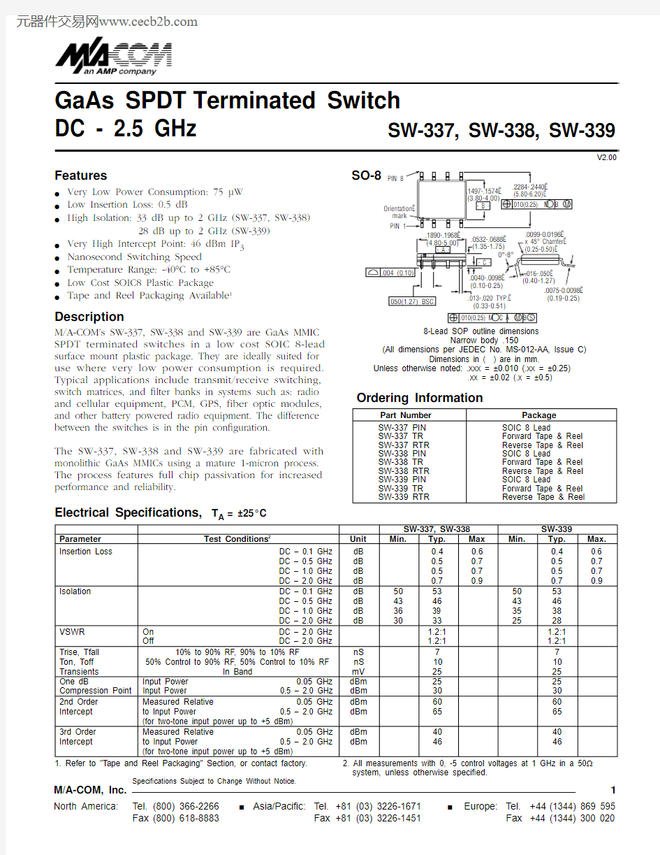
SO-8
(0.19-0.25)
Part Number Package SW-337 PIN SOIC 8 Lead
SW-337 TR Forward Tape & Reel SW-337 RTR Reverse Tape & Reel SW-338 PIN SOIC 8 Lead
SW-338 TR Forward Tape & Reel SW-338 RTR Reverse Tape & Reel SW-339 PIN SOIC 8 Lead
SW-339 TR Forward Tape & Reel SW-339 RTR
Reverse Tape & Reel
Ordering Information
SW-337, SW-338SW-339Parameter Test Conditions
2
Unit Min.Typ.Max
Min.
Typ.Max.Insertion Loss
DC – 0.1 GHz dB 0.40.60.40.6 DC – 0.5 GHz dB 0.50.70.50.7DC – 1.0 GHz dB 0.50.70.50.7DC – 2.0 GHz
dB 0.70.9
0.70.9
Isolation DC – 0.1 GHz
dB 50535053DC – 0.5 GHz dB 43464346DC – 1.0 GHz dB 3639 3538DC – 2.0 GHz
dB
3033
25
28VSWR On DC – 2.0 GHz
1.2:1 1.2:1Off DC –
2.0 GHz
1.2:1 1.2:1Trise, Tfall 10% to 90% RF, 90% to 10% RF nS 77Ton, Toff 50% Control to 90% RF, 50% Control to 10% RF nS 1010Transients In Band mV 2525One dB Input Power 0.05 GHz dBm 2525Compression Point Input Power 0.5 –
2.0 GHz dBm 30302nd Order Measured Relative 0.05 GHz dBm 6060Intercept to Input Power 0.5 – 2.0 GHz
dBm 65
65(for two-tone input power up to +5 dBm)
3rd Order Measured Relative 0.05 GHz dBm 4040Intercept to Input Power 0.5 – 2.0 GHz
dBm
46
46
(for two-tone input power up to +5 dBm)
1. Refer to "Tape and Reel Packaging" Section, or contact factory.
2. All measurements with 0, -5 control voltages at 1 GHz in a 50?system, unless otherwise speci?ed.
q q q
q q q q q
8-Lead SOP outline dimensions
Narrow body .150
(All dimensions per JEDEC No. MS-012-AA, Issue C)
Dimensions in ( ) are in mm.
Unless otherwise noted: .xxx = ±0.010 (.xx = ±0.25)
.xx = ±0.02 (.x = ±0.5)
元器件交易网https://www.360docs.net/doc/c115566410.html,
GaAs SPDT Terminated Switch SW-337, SW-338, SW-339
V2.00
M/A-COM, Inc.
2
Speci?cations Subject to Change Without Notice.
Parameter Absolute Maximum 1Max. Input Power 0.05 GHz +27 dBm 0.5 – 2.0 GHz +34 dBm Control Voltage +5V, -8.5V Operating Temperature -40°C to +85°C Storage Temperature
-65°C to +150°C
Absolute Maximum Ratings
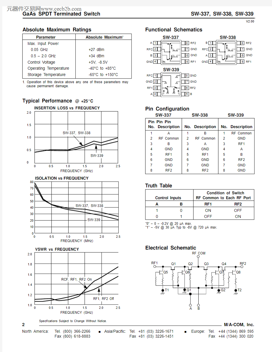
Pin Con?guration
SW-337
SW-338
SW-339
Truth Table
Typical Performance
@ +25°C
1. Operation of this device above any one of these parameters may
cause permanent damage.
RF1
GND GND RF2B A RF1
GND GND RF2A B B
RF2GND GND FREQUENCY (GHz)
2.0
1.5
1.0
0.5
0.5
1.0
1.5
2.0
2.5
L O S S (d B )
ISOLATION vs FREQUENCY
VSWR vs FREQUENCY
INSERTION LOSS vs FREQUENCY
FREQUENCY (GHz)
2.01.81.6
1.4
1.2
1.0
0.5
1.0
1.5
2.0
2.5
V S W R
8070
60504030201000
0.5
1.0
1.5
2.0
2.5
FREQUENCY (MHz)
I S O L A T I O N (d B )
Pin Pin Pin No.Description No.Description No.Description
1A
1B
1RF Common
2RF Common
2RF Common
2GND 3B 3A 3RF14GND 4GND 4A 5RF15RF15B 6GND 6GND 6RF27GND 7GND 7GND 8RF28RF28GND
Condition of Switch Control Inputs
RF Common to Each RF Port
A B RF1RF210ON OFF 0
1
OFF
ON
"0" – 0 – -0.2V @ 20 μA max.
"1" – -5V @ 30 μA Typ to -8V @ 720 μA max.
Functional Schematics
Electrical Schematic
元器件交易网https://www.360docs.net/doc/c115566410.html,