STE110NA20中文资料
STE110NA20
N -CHANNEL ENHANCEMENT MODE
FAST POWER MOS TRANSISTOR
PRELIMINARY DATA
s TYPICAL R DS(on)=0.015?
s HIGH CURRENT POWER MODULE s AVALANCHE RUGGED TECHNOLOGY
s
VERY LARGE SOA -LARGE PEAK POWER CAPABILITY
s EASY TO MOUNT
s
SAME CURRENT CAPABILITY FOR THE TWO SOURCE TERMINALS
s EXTREMELY LOW Rth (Junction to case)s
VERY LOW INTERNAL PARASITIC INDUCTANCE
s
ISOLATED PACKAGE UL RECOGNIZED
APPLICATIONS s SMPS &UPS s MOTOR CONTROL s WELDING EQUIPMENT s OUTPUT STAGE FOR PWM,ULTRASONIC CIRCUITS
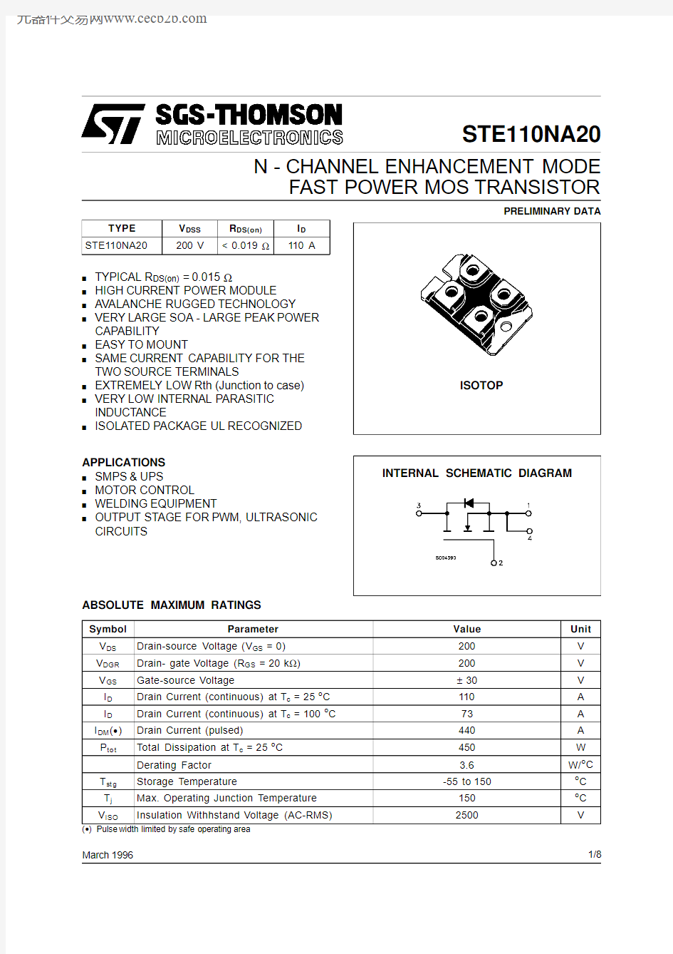
INTERNAL SCHEMATIC DIAGRAM
ABSOLUTE MAXIMUM RATINGS
Symbol Parameter
Value Unit V DS Drain-source Voltage (V GS =0)200V V DGR Drain-gate Voltage (R GS =20k ?)200V V GS Gate-source Voltage
±30V I D Drain Current (continuous)at T c =25o C 110A I D Drain Current (continuous)at T c =100o
C 73A I DM (?)Drain Current (pulsed)
440A P to t Total Dissipation at T c =25o
C 450W Derating Factor 3.6W/o
C
T st g Storage Temperature
-55to 150
o C T j Max.Operating Junction Temperature 150o C
V ISO
Insulation Withhstand Voltage (AC-RMS)
2500
V
(?)Pulse width limited by safe operating area
TYPE V DSS R DS(on)I D STE110NA20
200V
<0.019?
110A
March 1996ISOTOP
1/8
THERMAL DATA
R t hj-ca se R thc-h Thermal Resistance Junction-case Max
Thermal Resistance Case-heatsink With Conductive
Grease Applied Max
0.27
0.05
o C/W
o C/W
AVALANCHE CHARACTERISTICS
Symbol Parameter Max Value Unit
I AR Avalanche Current,Repetitive or Not-Repetitive
(pulse width limited by T j max,δ <1%)
55A
E AS Single Pulse Avalanche Energy
(starting T j=25o C,I D=I AR,V DD=50V)
500mJ
E AR Repetitive Avalanche Energy
(pulse width limited by T j max,δ <1%)
175mJ
I AR Avalanche Current,Repetitive or Not-Repetitive
(T c=100o C,pulse width limited by T j max,δ <1%)
32.5A
ELECTRICAL CHARACTERISTICS(T case=25o C unless otherwise specified)
OFF
Symbol Parameter Test Conditions Min.Typ.Max.Unit V(BR)DSS Drain-source
Breakdown Voltage
I D=1mA V GS=0200V
I DSS Zero Gate Voltage
Drain Current(V GS=0)V DS=Max Rating
V DS=Max Rating x0.8T c=125o C
400
200
μA
mA
I GSS Gate-body Leakage
Current(V DS=0)
V GS=±30V±400nA ON(?)
Symbol Parameter Test Conditions Min.Typ.Max.Unit V GS(th)Gate Threshold Voltage V DS=V GS I D=1mA 2.253 3.75V
R DS(on)Static Drain-source On
Resistance V GS=10V I D=55A
V GS=10V I D=55A T c=100o C
0.0150.019?
?
I D(o n)On State Drain Current V DS>I D(on)x R DS(on)max
V GS=10V
110A DYNAMIC
Symbol Parameter Test Conditions Min.Typ.Max.Unit
g fs(?)Forward
Transconductance
V DS=15V I D=55A38S
C iss C oss C rss Input Capacitance
Output Capacitance
Reverse Transfer
Capacitance
V DS=25V f=1MHz V GS=012.9
2870
980
nF
pF
pF
STE110NA20 2/8
ELECTRICAL CHARACTERISTICS(continued)
SWITCHING ON
Symbol Parameter Test Conditions Min.Typ.Max.Unit
t d(on) t r Turn-on Time
Rise Time
V DD=100V I D=55A
R G=4.7 ?V GS=10V
(see test circuit,figure3)
70
95
100
125
ns
ns
(di/dt)on Turn-on Current Slope V DD=160V I D=110A
R G=47 ?V GS=10V
(see test circuit,figure5)
290A/μs
Q g Q gs Q gd Total Gate Charge
Gate-Source Charge
Gate-Drain Charge
V DD=160V I D=110A V GS=10V470
43
226
600nC
nC
nC
SWITCHING OFF
Symbol Parameter Test Conditions Min.Typ.Max.Unit
t r(Vof f) t f
t c Off-voltage Rise Time
Fall Time
Cross-over Time
V DD=160V I D=110A
R G=4.7 ?V GS=10V
(see test circuit,figure5)
115
68
160
150
100
210
ns
ns
ns
SOURCE DRAIN DIODE
Symbol Parameter Test Conditions Min.Typ.Max.Unit
I SD I SDM(?)Source-drain Current
Source-drain Current
(pulsed)
110
440
A
A
V SD(?)Forward On Voltage I SD=110A V GS=0 1.6V
t rr Q rr I RRM Reverse Recovery
Time
Reverse Recovery
Charge
Reverse Recovery
Current
I SD=110A di/dt=100A/μs
V R=50V T j=150o C
(see test circuit,figure5)
625
11
35
ns
μC
A
(?)Pulsed:Pulse duration=300μs,duty cycle1.5%
(?)Pulse width limited by safe operating area
Safe Operating Area Thermal Impedance
STE110NA20
3/8
Derating Curve
Transfer Characteristics
Static Drain-source On Resistance Output Characteristics Transconductance
Gate Charge vs Gate-source Voltage
STE110NA20 4/8
Capacitance Variations
Normalized On Resistance vs Temperature Turn-off Drain-source Voltage Slope Normalized Gate Threshold Voltage vs Temperature
Turn-on Current Slope
Cross-over Time
STE110NA20
5/8
Switching Safe Operating Area
Source-drain Diode Forward Characteristics Fig.1:Unclamped Inductive Load Test Circuit Accidental Overload Area
Fig.2:Unclamped Inductive Waveform
STE110NA20 6/8
Fig.3:Switching Times Test Circuits For Resistive Load
Fig.5:Test Circuit For Inductive Load Switching And DIode Recovery Times Fig.4:Gate Charge test Circuit
STE110NA20
7/8
STE110NA20
Information furnished is believed to be accurate and reliable.However,SGS-THOMSON Microelectronics assumes no responsabilit y for the consequences of use of such information nor for any infringemen t of patents or other rights of third parties which may results from its use.No license is granted by implication or otherwise under any patent or patent rights of SGS-THOMSON Microelectr onics.Specifications mention ed in this publication are subject to change without notice.This publication supersede s and replaces all information previously supplied.
SGS-THOMSON Microelectr onics products are not auth orized for use as critical compon ents in life support devices or systems without expre ss written approval of SGS-THOMSON Microelectonics.
?1995SGS-THOMSON Microelectroni c s-All Rights Reserved
SGS-THOMSON Microelectronics GROUP OF COMPANIES
Australia-Brazil-France-Germany-Hong Kong-Italy-Japan-Korea-Malaysia-Malta-Morocco-The Netherlands-
Singapore-Spain-Sweden-Switzerland-Taiwan-Thailand-United Kingdom-U.S.A
...
8/8