LM4701单声道30W功放
LM4701Overture ?Audio Power Amplifier Series 30W Audio Power Amplifier with Mute and Standby Modes
General Description
The LM4701is an audio power amplifier capable of deliver-ing typically 30W of continuous average output power into an 8?load with less than 0.1%(THD +N).
The LM4701has an independent smooth transition fade-in/out mute and a power conserving standby mode which can be controlled by external logic.
The performance of the LM4701,utilizing its Self Peak In-stantaneous Temperature (?Ke)(SPiKe ?)Protection Cir-cuitry,places it in a class above discrete and hybrid amplifi-ers by providing an inherently,dynamically protected Safe Operating Area (SOA).SPiKe Protection means that these parts are completely safeguarded at the output against over-voltage,undervoltage,overloads,including thermal runaway and instantaneous temperature peaks.
Key Specifications
n THD+N at 1kHz at continuous average output power of 25W into 8?:0.1%(max)n THD+N from 20Hz to 20kHz at 30W of continuous average output power into 8?:0.08%(typ)n Standby current: 2.1mA (typ)
Features
n SPiKe Protection
n Minimal amount of external components necessary n Quiet fade-in/out mute function n Power conserving standby-mode n
Non-Isolated 9-lead TO-220package
Applications
n TVs
n Component stereo n Compact stereo
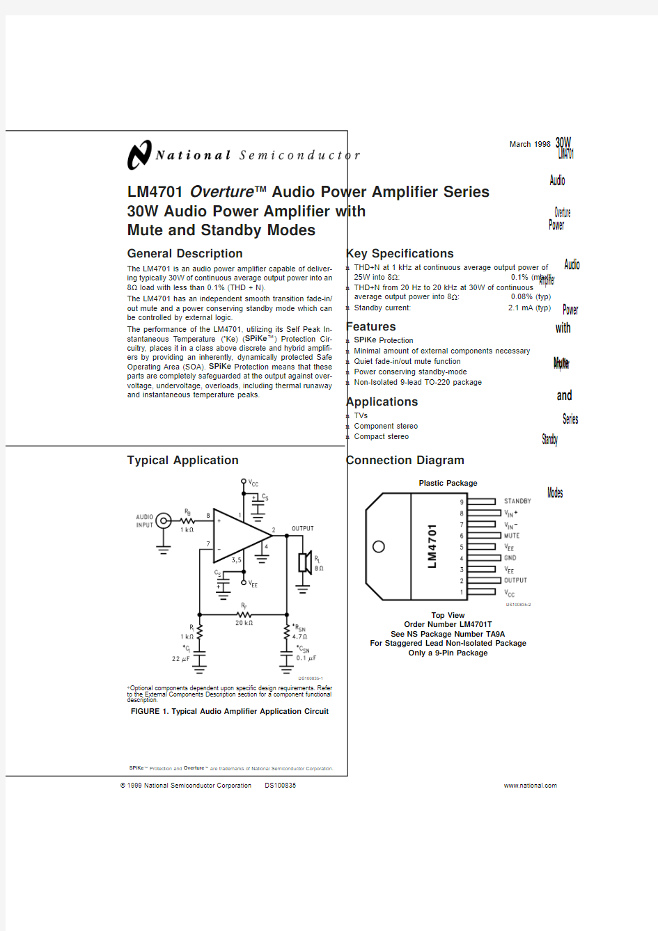
Typical Application Connection Diagram
SPiKe ?Protection and Overture ?are trademarks of National Semiconductor Corporation.
DS100835-1
*Optional components dependent upon specific design requirements.Refer
to the External Components Description section for a component functional description.
FIGURE 1.Typical Audio Amplifier Application Circuit
Plastic Package
DS100835-2
Top View
Order Number LM4701T See NS Package Number TA9A
For Staggered Lead Non-Isolated Package
Only a 9-Pin Package
March 1998
LM4701Overture Audio Power Amplifier Series 30W Audio Power Amplifier with Mute and Standby Modes
?1999National Semiconductor Corporation https://www.360docs.net/doc/df9590003.html,
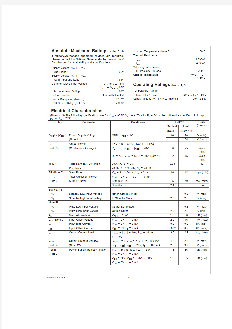
Absolute Maximum Ratings(Notes5,4) If Military/Aerospace specified devices are required, please contact the National Semiconductor Sales Office/ Distributors for availability and specifications.
Supply Voltage|V CC|+|V EE|
(No Signal)66V Supply Voltage|V CC|+|V EE|
(with Input and Load)64V Common Mode Input Voltage(V CC or V EE)and
|V CC|+|V EE|≤60V Differential Input Voltage60V Output Current Internally Limited Power Dissipation(Note6)62.5W ESD Susceptibility(Note7)2000V Junction Temperature(Note8)150?C Thermal Resistance
θJC 1.8?C/W θJA43?C/W Soldering Information
TF Package(10sec.)260?C Storage Temperature?40?C≤T A≤
+150?C Operating Ratings(Notes4,5)
Temperature Range
T MIN≤T A≤T MAX?20?C≤T A≤+85?C Supply Voltage|V CC|+|V EE|(Note1)20V to64V
Electrical Characteristics
(Notes4,5)The following specifications are for V CC=+28V,V EE=?28V with R L=8?,unless otherwise specified.Limits ap-ply for T A=25?C.
Symbol Parameter Conditions LM4701Units
(Limits)
Typical Limit
(Note9)(Note10)
|V CC|+|V EE|Power Supply Voltage GND?V EE≥9V1820V(min) (Note11)64V(max) P O Output Power THD+N=0.1%(max),f=1kHz
(Note3)(Continuous Average)R L=8?,|V CC|=|V EE|=28V3025W/ch
(min)
R L=4?,|V CC|=|V EE|=20V(Note13)2215W/ch
(min) THD+N Total Harmonic Distortion30W/ch,R L=8?,0.08% Plus Noise20Hz≤f≤20kHz,A V=26dB
SR(Note3)Slew Rate V IN=1.414Vrms,t rise=2ns1812V/μs(min) I TOTAL Total Quiescent Power V CM=0V,V O=0V,I O=0mA
(Note2)Supply Current Standby:Off2540mA(max)
Standby:On 2.1mA Standby Pin
V IL Standby Low Input Voltage Not in Standby Mode0.8V(max) V IH Standby High Input Voltage In Standby Mode 2.0 2.5V(min) Mute Pin
V IL Mute Low Input Voltage Output Not Muted0.8V(max) V IH Mute High Input Voltage Output Muted 2.0 2.5V(min) A M Mute Attenuation V PIN8=2.5V11580dB(min) V OS(Note2)Input Offset Voltage V CM=0V,I O=0mA 2.015mV(max) I B Input Bias Current V CM=0V,I O=0mA0.20.5μA(max) I OS Input Offset Current V CM=0V,I O=0mA0.0020.2μA(max) I O Output Current Limit|V CC|=|V EE|=10V,t ON=10ms, 3.5 2.9A PK(min)
V O=0V
V OD Output Dropout Voltage|V CC?V O|,V CC=20V,I O=+100mA 1.8 2.3V(max) (Note2)(Note12)|V O?V EE|,V EE=?20V,I O=?100mA 2.5 3.2V(max) PSRR Power Supply Rejection Ratio V CC=30V to10V,V EE=?30V,11585dB(min) (Note2)V CM=0V,I O=0mA
V CC=30V,V EE=?30V to?10V11085dB(min)
V CM=0V,I O=0mA
https://www.360docs.net/doc/df9590003.html,2
Electrical Characteristics(Continued)
(Notes4,5)The following specifications are for V CC=+28V,V EE=?28V with R L=8?,unless otherwise specified.Limits ap-ply for T A=25?C.
Symbol Parameter Conditions LM4701Units
(Limits)
Typical Limit
(Note9)(Note10)
CMRR(Note 2)Common Mode Rejection Ratio V CC=35V to10V,V EE=?10V to?35V,11080dB(min)
V CM=10V to?10V,I O=0mA
A VOL(Note2)Open Loop Voltage Gain R L=2k?,?V O=30V11090dB(min) GBWP Gain-Bandwidth Product f O=100kHz,V IN=50mVrms7.55MHz(min) e IN Input Noise IHF—A Weighting Filter 2.08μV(max) (Note3)R IN=600?(Input Referred)
SNR Signal-to-Noise Ratio P O=1W,A-Weighted,98dB
Measured at1kHz,R S=25?
P O=25W,A-Weighted108dB
Measured at1kHz,R S=25?
Note1:Operation is guaranteed up to64V,however,distortion may be introduced from SPiKe Protection Circuitry if proper thermal considerations are not taken into account.Refer to the Application Information section for a complete explanation.
Note2:DC Electrical Test;Refer to Test Circuit#1.
Note3:AC Electrical Test;Refer to Test Circuit#2.
Note4:All voltages are measured with respect to the GND(pin7),unless otherwise specified.
Note5:Absolute Maximum Ratings indicate limits beyond which damage to the device may occur.Operating Ratings indicate conditions for which the device is func-tional,but do not guarantee specific performance limits.Electrical Characteristics state DC and AC electrical specifications under particular test conditions which guar-antee specific performance limits.This assumes that the device is within the Operating Ratings.Specifications are not guaranteed for parameters where no limit is given,however,the typical value is a good indication of device performance.
Note6:For operating at case temperatures above25?C,the device must be derated based on a150?C maximum junction temperature and a thermal resistance of θJC=1.8?C/W(junction to case).Refer to the section,Determining the Correct Heat Sink,in the Application Information section.
Note7:Human body model,100pF discharged through a1.5k?resistor.
Note8:The operating junction temperature maximum is150?C,however,the instantaneous Safe Operating Area temperature is250?C.
Note9:Typicals are measured at25?C and represent the parametric norm.
Note10:Limits are guarantees that all parts are tested in production to meet the stated values.
Note11:V EE must have at least?9V at its pin with reference to ground in order for the under-voltage protection circuitry to be disabled.In addition,the voltage dif-ferential between V CC and V EE must be greater than14V.
Note12:The output dropout voltage,V OD,is the supply voltage minus the clipping voltage.Refer to the Clipping Voltage vs.Supply Voltage graph in the Typical Per-formance Characteristics section.
Note13:For a4?load,and with±20V supplies,the LM4701can deliver typically22Watts of continuous average power per channel with less than0.1%(THD+N).
With supplies above±20V,the LM4701cannot deliver more than22watts into4?due to current limiting of the output transistors.Thus,increasing the power supply above±20V will only increase the internal power dissipation,not the possible output power.Increased power dissipation will require a larger heat sink as explained in the Application Information section.
https://www.360docs.net/doc/df9590003.html,
3
Test Circuit #1
(Note 2)(DC Electrical Test Circuit)
Test Circuit #2
(Note 3)(AC Electrical Test Circuit)
Bridged Amplifier Application Circuit
DS100835-3
DS100835-4
DS100835-5
FIGURE 2.Bridged Amplifier Application Circuit
https://www.360docs.net/doc/df9590003.html, 4
Single Supply Application Circuit
Auxillary Amplifier Application Circuit
DS100835-6
FIGURE 3.Single Supply Amplifier Application Circuit
DS100835-7
FIGURE 4.Auxillary Amplifier Application Circuit
https://www.360docs.net/doc/df9590003.html,
5
Equivalent Schematic(Excluding Active Protection Circuitry)
DS100835-8 https://www.360docs.net/doc/df9590003.html,6
External Components Description
Components Functonal Description
1R B Prevents currents from entering the amplifier’s non-inverting input which may be passed through to the load upon power down of the system due to the low input impedance of the circuitry when the
undervoltage circuitry is off.This phenomenon occurs when the supply voltages are below1.5V.
2R I Inverting input resistance to provide AC gain in conjunction with R F.Also creates a highpass filter with C I at f C=1/(2πR I C I).
3R F Feedback resistance to provide AC gain in conjunction with R I.
4C I(Note14)Feedback capacitor which ensures unity gain at DC.
5C S Provides power supply filtering and bypassing.Refer to the Supply Bypassing application section for proper placement and selection of bypass capacitors.
6R V
(Note14)
Acts as a volume control by setting the input voltage level.
7R IN
(Note14)Sets the amplifier’s input terminals DC bias point when C IN is present in the circuit.Also works with C IN to create a highpass filter at f C=1/(2πR IN C IN).Refer to Figure4.
8C IN
(Note14)
Input capacitor which blocks the input signal’s DC offsets from being passed onto the amplifier’s inputs.
9R SN
(Note14)Works with C SN to stabilize the output stage by creating a pole that reduces high frequency instabilities. The pole is set at f C=1/(2πR SN C SN).Refer to Figure4.
10C SN
(Note14)
Works with R SN to stabilize the output stage by creating a pole that reduces high frequency instabilities.
11L(Note14)Provides high impedance at high frequencies so that R may decouple a highly capacitive load and reduce the Q of the series resonant circuit.Also provides a low impedance at low frequencies to short
out R and pass audio signals to the load.Refer to Figure4.
12R(Note14)
13R A Provides DC voltage biasing for the transistor Q1in single supply operation.
14C A Provides bias filtering for single supply operation.
15R INP
(Note14)Limits the voltage difference between the amplifier’s inputs for single supply operation.Refer to the Clicks and Pops application section for a more detailed explanation of the function of R INP.
16R BI Provides input bias current for single supply operation.Refer to the Clicks and Pops application section for a more detailed explanation of the function of R BI.
17R E Establishes a fixed DC current for the transistor Q1in single supply operation.This resistor stabilizes the half-supply point along with C A.
Note14:Optional components dependent upon specific design requirements.
https://www.360docs.net/doc/df9590003.html,
7
Typical Performance Characteristics
THD +N vs Frequency
DS100835-10THD +N vs Frequency
DS100835-11THD +N vs Frequency
DS100835-12
THD +N vs Output Power DS100835-13THD +N vs Output Power DS100835-14THD +N vs Output Power
DS100835-15
THD +N vs Output Power DS100835-16THD +N vs Output Power DS100835-17THD +N vs Output Power
DS100835-18
Clipping Voltage vs Supply Voltage
DS100835-19
Clipping Voltage vs Supply Voltage
DS100835-20
Clipping Voltage vs Supply Voltage
DS100835-21
https://www.360docs.net/doc/df9590003.html, 8
Typical Performance Characteristics(Continued)
Power Dissipation vs
Output Power
DS100835-22Power Dissipation vs
Ouput Power
DS100835-23
Power Dissipation vs
Output Power
DS100835-24
Output Power vs
Load Resistance
DS100835-25Output Power vs
Supply Voltage
DS100835-26
Output Mute vs
Mute Pin Voltage
DS100835-27
Pulse Response
DS100835-28Large Signal Response
DS100835-29
Output Mute vs
Mute Pin Voltage
DS100835-30
https://www.360docs.net/doc/df9590003.html, 9
Typical Performance Characteristics
(Continued)
Power Supply Rejection Ratio
DS100835-31
Common-Mode Rejection Ratio
DS100835-32
Open Loop
Frequency Response
DS100835-33
Safe Area DS100835-34
Spike Protection Response
DS100835-35
Supply Current vs Supply Voltage
DS100835-36
Pulse Thermal Resistance
DS100835-37
Pulse Thermal Resistance
DS100835-38Supply Current vs Output Voltage
DS100835-39
https://www.360docs.net/doc/df9590003.html, 10
Typical Performance Characteristics(Continued)
Application Information
MUTE MODE
By placing a logic-high voltage on the mute pin,the signal going into the amplifiers will be muted.If the mute pin is left floating or connected to a logic-low level,the amplifier will be in a non-muted state.Refer to the Typical Performance Characteristics section for curves concerning Mute Attenu-ation vs Mute Pin Voltage.
STANDBY MODE
The standby mode of the LM4701allows the user to drasti-cally reduce power consumption when the amplifier is idle. By placing a logic-high voltage on the standby pin,the ampli-fier will go into Standby Mode.In this mode,the current drawn from the V CC supply is typically less than10μA total for both amplifiers.The current drawn from the V EE supply is typically2.1mA.Clearly,there is a significant reduction in idle power consumption when using the standby mode.Re-fer to the Typical Performance Characteristics section for curves showing Supply Current vs Standby Pin Voltage for both supplies.
UNDER-VOLTAGE PROTECTION
Upon system power-up,the under-voltage protection cir-cuitry allows the power supplies and their corresponding ca-pacitors to come up close to their full values before turning on the LM4701such that no DC output spikes occur.Upon turn-off,the output of the LM4701is brought to ground be-fore the power supplies such that no transients occur at power-down.
OVER-VOLTAGE PROTECTION
The LM4701contains over-voltage protection circuitry that limits the output current to approximately3.5Apk while also providing voltage clamping,though not through internal clamping diodes.The clamping effect is quite the same, however,the output transistors are designed to work alter-nately by sinking large current spikes.
SPiKe PROTECTION
The LM4701is protected from instantaneous peak-temperature stressing of the power transistor array. The Safe Operating Area graph in the Typical Performance Characteristics section shows the area of device operation where SPiKe Protection Circuitry is not enabled.The wave-form to the right of the SOA graph exemplifies how the dy-namic protection will cause waveform distortion when en-abled.
THERMAL PROTECTION
The LM4701has a sophisticated thermal protection scheme to prevent long-term thermal stress of the device.When the temperature on the die reaches165?C,the LM4701shuts down.It starts operating again when the die temperature drops to about155?C,but if the temperature again begins to rise,shutdown will occur again at165?C.Therefore,the de-vice is allowed to heat up to a relatively high temperature if
Pulse Power Limit
DS100835-40Pulse Power Limit
DS100835-41
Supply Current vs
Case Temperature
DS100835-42
Standby Current(I CC)vs Standby Pin Voltage
DS100835-43Supply Current(I EE)vs
Standby Pin Voltage
DS100835-44
Input Bias Current vs
Case Temperature
DS100835-45
https://www.360docs.net/doc/df9590003.html, 11
Application Information(Continued)
the fault condition is temporary,but a sustained fault will cause the device to cycle in a Schmitt Trigger fashion be-tween the thermal shutdown temperature limits of165?C and 155?C.This greatly reduces the stress imposed on the IC by thermal cycling,which in turn improves its reliability under sustained fault conditions.
Since the die temperature is directly dependent upon the heat sink used,the heat sink should be chosen such that thermal shutdown will not be reached during normal https://www.360docs.net/doc/df9590003.html,ing the best heat sink possible within the cost and space constraints of the system will improve the long-term reliability of any power semiconductor device,as discussed in the Determining the Correct Heat Sink Section. DETERMINING MAXIMUM POWER DISSIPATION
Power dissipation within the integrated circuit package is a very important parameter requiring a thorough understand-ing if optimum power output is to be obtained.An incorrect maximum power dissipation calculation may result in inad-equate heat sinking causing thermal shutdown and thus lim-iting the output power.
Equation(1)exemplifies the theoretical maximum power dis-sipation point of each amplifier where V CC is the total supply voltage.
P DMAX=V CC2/2π2R L(1) Thus by knowing the total supply voltage and rated output load,the maximum power dissipation point can be calcu-lated.Refer to the graphs of Power Dissipation vs Output Power in the Typical Performance Characteristics section which show the actual full range of power dissipation not just the maximum theoretical point that results from equation(1). DETERMINING THE CORRECT HEAT SINK
The choice of a heat sink for a high-power audio amplifier is made entirely to keep the die temperature at a level such that the thermal protection circuitry does not operate under normal circumstances.
The thermal resistance from the die(junction)to the outside air(ambient)is a combination of three thermal resistances,θJC,θCS andθSA.The thermal resistance,θJC(junction to case),of the LM4701is2?C/https://www.360docs.net/doc/df9590003.html,ing Thermalloy Therma-cote thermal compound,the thermal resistance,θCS(case to sink),is about0.2?C/W.Since convection heat flow(power dissipation)is analogous to current flow,thermal resistance is analogous to electrical resistance,and temperature drops are analogous to voltage drops,the power dissipation out of the LM4701is equal to the following:
P DMAX=(T JMAX?T AMB)/θJA(2) where T JMAX=150?C,T AMB is the system ambient tempera-ture andθJA=θJC+θCS+θSA.
Once the maximum package power dissipation has been calculated using equation(1),the maximum thermal resis-tance,θSA,(in?C/W)for a heat sink can be calculated.This calculation is made using equation(3)which is derived by solving forθSA in equation(2).
θSA=[(T JMAX?T AMB)?P DMAX(θJC+θCS)]/P DMAX(3) Again it must be noted that the value ofθSA is dependent upon the system designer’s amplifier requirements.If the ambient temperature that the audio amplifier is to be working under is higher than25?C,then the thermal resistance for the heat sink,given all other things are equal,will need to be smaller.SUPPLY BYPASSING
The LM4701has excellent power supply rejection and does not require a regulated supply.However,to improve system performance as well as eliminate possible oscillations,the LM4701should have its supply leads bypassed with low-inductance capacitors having short leads that are lo-cated close to the package terminals.Inadequate power supply bypassing will manifest itself by a low frequency oscil-lation known as“motorboating”or by high frequency insta-bilities.These instabilities can be eliminated through multiple bypassing utilizing a large tantalum or electrolytic capacitor (10μF or larger)which is used to absorb low frequency variations and a small ceramic capacitor(0.1μF)to prevent any high frequency feedback through the power supply lines. If adequate bypassing is not provided,the current in the sup-ply leads which is a rectified component of the load current may be fed back into internal circuitry.This signal causes distortion at high frequencies requiring that the supplies be bypassed at the package terminals with an electrolytic ca-pacitor of470μF or more.
BRIDGED AMPLIFIER APPLICATION
One common power amplifier configuration is shown in Fig-ure2and is referred to as“bridged mode”operation.Bridged mode operation is different from the classical single-ended amplifier configuration where one side of the output load is connected to ground.
A bridge amplifier design has a distinct advantage over the single-ended configuration,as it provides differential drive to the load,thus doubling output swing for a specified supply voltage.Consequently,theoretically four times the output power is possible as compared to a single-ended amplifier under the same conditions.This increase in attainable output power assumes that the amplifier is not current limited or clipped.
A direct consequence of the increased power delivered to the load by a bridge amplifier is an increase in internal power dissipation.For each operational amplifier in a bridge con-figuration,the internal power dissipation will increase by a factor of two over the single ended dissipation.Since there are two amplifiers used in a bridge configuration,the maxi-mum system power dissipation point will increase by a factor of four over the figure obtained by equation(1).
This value of P DMAX can be used to calculate the correct size heat sink for a bridged amplifier application,assuming that both IC’s are mounted on the same heatsink.Since the inter-nal dissipation for a given power supply and load is in-creased by using bridged-mode,the heatsink’sθSA will have to decrease accordingly as shown by equation(3).Refer to the section,Determining the Correct Heat Sink,for a more detailed discussion of proper heat sinking for a given appli-cation.
SINGLE-SUPPLY AMPLIFIER APPLICATION
The typical application of the LM4701is a split supply ampli-fier.But as shown in Figure3,the LM4701can also be used in a single power supply configuration.This involves using some external components to create a half-supply bias which is used as the reference for the inputs and outputs. Thus,the signal will swing around half-supply much like it swings around ground in a split-supply application.Along with proper circuit biasing,a few other considerations must be accounted for to take advantage of all of the LM4701 functions.
https://www.360docs.net/doc/df9590003.html,12
Application Information
(Continued)
The LM4701possesses a mute and standby function with in-ternal logic gates that are half-supply referenced.Thus,to enable either the mute or standby function,the voltage at these pins must be a minimum of 2.5V above half-supply.In single-supply systems,devices such as microprocessors and simple logic circuits used to control the mute and standby functions,are usually referenced to ground,not half-supply.Thus,to use these devices to control the logic circuitry of the LM4701,a “level shifter”,like the one shown in Figure 5,must be employed.A level shifter is not needed in a split-supply configuration since ground is also half-supply.
When the voltage at the Logic Input node is 0V,the 2N3904is “off”and thus resistor R C pulls up mute or standby input to the supply.This enables the mute or standby function.When the Logic Input is 5V,the 2N3904is “on”and consequently,the voltage at the collector is essentially 0V.This will disable the mute or standby function,and thus the amplifier will be in its normal mode of operation.R SHIFT ,along with C SHIFT ,cre-ates an RC time constant that reduces transients when the mute or standby functions are enabled or disabled.Addition-ally,R SHIFT limits the current supplied by the internal logic gates of the LM4701which insures device reliability.Refer to the Mute Mode and Standby Mode sections in the Applica-tion Information section for a more detailed description of these functions.
CLICKS AND POPS
In the typical application of the LM4701as a split-supply au-dio power amplifier,the IC exhibits excellent “click”and “pop”performance when utilizing the mute and standby functions.In addition,the device employs Under-Voltage Protection,which eliminates unwanted power-up and power-down tran-sients.The basis for these functions are a stable and con-stant half-supply potential.In a split-supply application,ground is the stable half-supply potential.But in a single-supply application,the half-supply needs to charge up just like the supply rail,V CC .
This makes the task of attaining a clickless and popless turn-on more challenging.Any uneven charging of the ampli-fier inputs will result in output clicks and pops due to the dif-ferential input topology of the LM4701.
To achieve a transient free power-up and power-down,the voltage seen at the input terminals should be ideally the same.Such a signal will be common-mode in nature,and will be rejected by the LM4701.In Figure 3,the resistor R INP serves to keep the inputs at the same potential by limiting the voltage difference possible between the two nodes.This should significantly reduce any type of turn-on pop,due to an uneven charging of the amplifier inputs.This charging is
based upon a specific application loading and thus,the sys-tem designer may need to adjust these values for optimum performance.
As shown in Figure 3,the resistors labeled R BI help bias up the LM4701off the half-supply node at the emitter of the 2N3904.But due to the input and output coupling capacitors in the circuit,along with the negative feedback,there are two different values of R BI ,namely 10k ?and 200k ?.These re-sistors bring up the inputs at the same rate resulting in a pop-less turn-on.Adjusting these resistors values slightly may re-duce pops resulting from power supplies that ramp extremely quick or exhibit overshoot during system turn-on.AUDIO POWER AMPLlFIER DESIGN Design a 25W/8?Audio Amplifier Given:
Power Output 25Wrms
Load Impedance 8?
Input Level 1Vrms(max)
Input Impedance
47k ?
Bandwidth 20Hz to 20kHz ±0.25dB A designer must first determine the power supply require-ments in terms of both voltage and current needed to obtain the specified output power.V OPEAK can be determined from equation (4)and I OPEAK from equation (5).
(4)(5)
To determine the maximum supply voltage,the following conditions must be considered.Add the dropout voltage to the peak output swing V OPEAK ,to get the supply rail at a cur-rent of I OPEAK .The regulation of the supply determines the unloaded voltage which is usually about 15%higher.The supply voltage will also rise 10%during high line conditions.Therefore the maximum supply voltage is obtained from the following equation:
Max Supplies ≈±(V OPEAK +V OD )(1+Regulation)(1.1)For 25W of output power into an 8?load,the required V O -PEAK is 20V.A minimum supply rail of ±25V results from add-ing V OPEAK and V OD .With regulation,the maximum supplies are ±31.7V and the required I OPEAK is 2.5A from equation (5).At this point it is a good idea to check the Power Output vs Supply Voltage to ensure that the required output power is obtainable from the device while maintaining low THD+N.In addition,the designer should verify that with the required power supply voltage and load impedance,that the required heatsink value θSA is feasible given system cost and size constraints.Once the heatsink issues have been addressed,the required gain can be determined from equation (6).(6)
From equation (6),the minimum A V is A V ≥14.14.
By selecting a gain of 21,and with a feedback resistor,R F =20k ?,the value of R I follows from equation (7).
R I =R F (A V ?1)
(7)Thus with R J =1k ?a non-inverting gain of 21will result.Since the desired input impedance was 47k ?,a value of 47k ?was selected for R IN .The final design step is to address the bandwidth requirements which must be stated as a pair of ?3dB frequency points.Five times away from a ?3dB
DS100835-9
FIGURE 5.Level Shift Circuit
https://www.360docs.net/doc/df9590003.html,
13
Application Information(Continued)
point is0.17dB down from passband response which is bet-ter than the required±0.25dB specified.This fact results in a low and high frequency pole of4Hz and100kHz respec-tively.As stated in the External Components section,R I in conjunction with C I create a high-pass filter.
C I≥1/(2π*1k?*4Hz)=39.8μF;use39μF.The high frequency pole is determined by the product of the desired high frequency pole,f H,and the gain,A V.With a A V =21and f
H
=100kHz,the resulting GBWP of2.1MHz is less than the minimum GBWP of5MHz for the LM4701.This will ensure that the high frequency response of the amplifier will be no worse than0.17dB down at20kHz which is well within the bandwidth requirements of the design.
https://www.360docs.net/doc/df9590003.html,14
Physical Dimensions inches(millimeters)unless otherwise noted
LIFE SUPPORT POLICY
NATIONAL’S PRODUCTS ARE NOT AUTHORIZED FOR USE AS CRITICAL COMPONENTS IN LIFE SUPPORT
DEVICES OR SYSTEMS WITHOUT THE EXPRESS WRITTEN APPROVAL OF THE PRESIDENT AND GENERAL
COUNSEL OF NATIONAL SEMICONDUCTOR CORPORATION.As used herein:
1.Life support devices or systems are devices or
systems which,(a)are intended for surgical implant
into the body,or(b)support or sustain life,and
whose failure to perform when properly used in
accordance with instructions for use provided in the
labeling,can be reasonably expected to result in a
significant injury to the user.
2.A critical component is any component of a life
support device or system whose failure to perform
can be reasonably expected to cause the failure of
the life support device or system,or to affect its
safety or effectiveness.
National Semiconductor
Corporation
Americas
Tel:1-800-272-9959
Fax:1-800-737-7018
Email:support@https://www.360docs.net/doc/df9590003.html,
National Semiconductor
Europe
Fax:+49(0)180-5308586
Email:europe.support@https://www.360docs.net/doc/df9590003.html,
Deutsch Tel:+49(0)180-5308585
English Tel:+49(0)180-5327832
Fran?ais Tel:+49(0)180-5329358
Italiano Tel:+49(0)180-5341680
National Semiconductor
Asia Pacific Customer
Response Group
Tel:65-2544466
Fax:65-2504466
Email:sea.support@https://www.360docs.net/doc/df9590003.html,
National Semiconductor
Japan Ltd.
Tel:81-3-5639-7560
Fax:81-3-5639-7507 https://www.360docs.net/doc/df9590003.html,
For Staggered Lead Non-Isolated Package
Only a9-Pin Package
Order Number LM4701T
NS Package Number TA9A
LM4701
Overture
Audio
Power
Amplifier
Series
30W
Audio
Power
Amplifier
with
Mute
and
Standby
Modes National does not assume any responsibility for use of any circuitry described,no circuit patent licenses are implied and National reserves the right at any time without notice to change said circuitry and specifications.
This datasheet has been downloaded from:
https://www.360docs.net/doc/df9590003.html,
Free Download
Daily Updated Database
100% Free Datasheet Search Site
100% Free IC Replacement Search Site
Convenient Electronic Dictionary
Fast Search System
https://www.360docs.net/doc/df9590003.html,
All Datasheets Cannot Be Modified Without Permission
Copyright ? Each Manufacturing Company
专业功率放大器桥接单声道输出如何使用
专业功率放大器桥接单声道输出如何使用 专业功率放大器在桥接单声道输出模式,工作模式选择开关打向桥接单声道输出(BTL)模式,输入信号从功率放大器的左声道输入口加入,用左声道音量控制旋钮(LEVEL)同时控制左声道、右声道两路输出信号的电压大小,此时右声道输入口和音量控制旋钮(LEVEL)的信号通路都已在内部被开关切断,左声道输出的是与输入信号同相位、幅度被放大了的信号,右声道输出的是与输入信号反相位、幅度与左声道输出信号幅度绝对值相同的信号,如图5-3中标有BTL文字所指两路波形。这种输出模式也只要一路输入信号即可,通常在音箱额定输入电功率很大时使用,用一台立体声功率放大器的两路功率放大器共同推动一只音箱,由于左声道、右声道输出是同幅度、反相位,所以加到音箱上的电压是单路输出电压的2倍,那么功率就是4倍了,所以一般应该将左声道的音量控制旋钮(LEVEL)从最小开始慢慢往大调节,到音量满足要求为止。从波形图中看到,由于左声道功率放大器的输出是与输入信号同相位的,所以左声道功率放大器的红色(正端)输出接线柱应该接音箱的红色接线柱(正端),右声道功率放大器的红色(正端)输出接线柱应该接音箱的黑色接线柱(负端),接线示意图如图所示。由于一台立体声功率放大器只能推动一只音箱,所以一对音箱就需要两台相同的立体声功率放大器来推动,但是接线时不论推动的是左音箱,还是右音箱,接线方法都是左声道功率放大器的红色(正端)输出接线柱应该接音箱的红色接线柱(正端),右声道功率放大器的红色(正端)输出接线柱应该接音箱的黑色接线柱(负端),其区分左、右声道的是前面设备输出的是左声道信号,还是右声道信号加到处于BTL工作模式的立体声功率放大器,如果是取自前面设备的左声道信号,则功放输出用来推动左音箱,反之,如果是取自前面设备的右声道信号,则功放输出用来推动右 音箱。 收藏分享
功放与音箱匹配技巧与注意事项
功放与音箱匹配技巧与注意事项 对功放与音响之间的匹配问题,除了音色软搭配之外(音色搭配常说软硬之分,是根据设计者对音色走向的设计和用料,而具有的特征和个性)还有一些技术指标上的硬搭配。软搭配是经验积累和个人爱好以实际感受为主,硬搭配则以数据和基本技术常识来定夺,下列就来简述硬搭配有关方面的问题。 阻抗匹配 1. 真空管功放(胆机)与音箱匹配时,放大器的输出阻抗应与音箱阻抗相等,否则会出现降低输出功率和增大失真等现象。好在大都胆机都有可变输出阻抗匹配接口如4-8-16欧,与音箱阻抗匹配已趋简单。 2. 对于晶体管功放(石机)与音箱阻抗的匹配 A) 音箱阻抗比功放输出阻抗高时,除了输出功率不同程度的降低外,无其它影响。 B) 音箱阻抗比功放输出阻抗低时,输出功率相应成比例增加,失真度一般不会增加或增加一点点可忽略。但匹配时音箱阻抗不能太低,如低至2奥姆(指2只4奥姆音箱并联时),此时只有功放功率富裕量大,并使用性能良好的大功率管和多管并联推挽,一般对这样的功放无影响。反之,一般普通功放富裕量不大,而功放管的pcm、lcm不大,当音量又开得很大时,这时失真会明显增大,严重时机毁箱亡,切切注意。 功率匹配
1、从原则上来讲,音箱额定功率与功放额定功率不一致时,对于功放来说,它的功率大小只与音箱阻抗有关,而与音箱额定功率无关。无论音箱功率与功放功率是否相同,对功放工作无影响,只是对音箱本身安全有关。 2、如果音箱阻抗符合匹配要求,而承受功率比功放功率小,则推动功率充足,听起来很舒服。这就是常说的功放储备功率要大,才能充分地表现出音乐全部内涵,尤其是音乐中的低频部分,表现更为生动、有力。这是一种较好的匹配。 3、如果音箱的额定阻抗大于功放的额定功率,虽然二者都能安全的工作,但这时功率放大器推动功率显得不够,会觉得响度不足,往往出现已经开到饱和状态,失真加剧,仍感到力不从心。这是一种较差的匹配。 按阻尼系数匹配
3W单声道AB类音频功率放大器
3W单声道AB类音频功率放大器 概述 LPA4871是一款3W、单声道AB类音频功率放大器。工作电压2.5-5.5V,以BTL桥接方式,在5V电源供电情况下,可以给4Ω负载提供THD小于10%、平均3.0W的输出功率。在关断模式下,电流典型值小于0.5μA。 LPA4871是为提供足功率、高保真音频输出而专门设计的,它仅需少量的外围器件,输出不需要外接耦合电容或上举电容,采用SOP-8封装,节约电路面积,非常适合移动电话及各种移动设备等使用低电压、低功耗应用方案上使用。 应用 ◆移动电话(手机等) ◆扩音器,蓝牙音响等 ◆收音机 ◆GPS,电子狗,行车记录仪 ◆语音玩具等特征 ◆工作电压:2.5 - 5.5V ◆创新的“开关/切换噪声”抑制技术,杜绝了上电、 掉电出现的噪声 ◆10% THD+N,VDD=5V,4Ω负载下,提供高达 2.9W的输出功率 ◆10% THD+N,VDD=5V,8Ω负载下,提供高达 1.8W的输出功率 ◆关断电流< 0.5μA ◆过温保护 ◆SOP-8封装 订购信息 LPA4871□□□ F: 无铅 封装类型 SO: SOP-8
封装及引脚配置 Bypass +IN -IN GND VDD VO1 VO2 图1. LPA4871的管脚定义图 典型应用电路 音频输入
音频输入 图3. LPA4871差分输入模式电路图 最大额定值 附注1:最大功耗取决于三个因素:T JMAX ,T A ,θJA ,它的计算公式P DMAX =(T JMAX -T A )/θJA ,LPA4871的T JMAX =150℃。T A 为外部环境的温度,θJA 取决于不同的封装形式。(SOP 封装形式为140℃/W )
功放与音箱的阻抗匹配
浅析功放与音箱匹配技巧与注意事项 6月2日报道对功放与音响之间的匹配问题,除了音色软搭配之外(音色搭配常说软硬之分,是根据设计者对音色走向的设计和用料,而具有的特征和个性)还有一些技术指标上的硬搭配。软搭配是经验积累和个人爱好以实际感受为主,硬搭配则以数据和基本技术常识来定夺,下列就来简述硬搭配有关方面的问题。 一、阻抗匹配 1、电子管功放(胆机)与音箱匹配时,放大器的输出阻抗应与音箱阻抗相等,否则会出现降低输出功率和增大失真等现象。好在大都胆机都有可变输出阻抗匹配接口如4-8-16欧,与音箱阻抗匹配已趋简单。 2、对于晶体管功放(石机)与音箱阻抗的匹配 ①音箱阻抗比功放输出阻抗高时,除了输出功率不同程度的降低外,无其它影响。 ②音箱阻抗比功放输出阻抗低时,输出功率相应成比例增加,失真度一般不会增加或增加一点点可忽略。但匹配时音箱阻抗不能太低,如低至2欧(指2只4欧音箱并联时),此时只有功放功率富裕量大,并使用性能良好的大功率管和多管并联推挽,一般对这样的功放无影响。反之,一般普通功放富裕量不大,而功放管的pcm、lcm不大,当音量又开得很大时,这时失真会明显增大,严重时机毁箱亡,切切注意。 二、功率匹配 1、从原则上来讲,音箱额定功率与功放额定功率不一致时,对于功放来说,它的功率大小只与音箱阻抗有关,而与音箱额定功率无关。无论音箱功率与功放功率是否相同,对功放工作无影响,只是对音箱本身安全有关。 2、如果音箱阻抗符合匹配要求,而承受功率比功放功率小,则推动功率充足,听起来很舒服。这就是常说的功放储备功率要大,才能充分地表现出音乐全部内涵,尤其是音乐中的低频部分,表现更为生动、有力。这是一种较好的匹配。 3、如果音箱的额定阻抗大于功放的额定功率,虽然二者都能安全的工作,但这时功率放大器推动功率显得不够,会觉得响度不足,往往出现已经开到饱和状态,失真加剧,仍感到力不从心。这是一种较差的匹配。 三、按阻尼系数匹配 对于选一对hi-fi音箱来讲,应有最佳的特定的电阻尼要求(负责任的音箱厂家应该提供此数据,指的是对功放阻尼系数的要求。说清楚点就是如要配此音箱,要求所配的功放阻尼系数要达到多少)。一般情况下,功放的阻尼系数高一点为好,低档功放阻尼系数小于10时,音箱的低频特征,输出特征,高次谐波特征等都会变坏。(家用功放的阻尼数一般在几十至几百之间。) 四、线材的匹配。 进口发烧线、神经线林林总总,贵至万余元,次之也要千元至数千元,(当然也有百元以下的),使用效果那是见仁见智的事。好的线材一般情况下都会改善音响器材中某系不足。它的传输理论说起来太复杂,只能简述了。传输线的材料与结构,决定了三个重要参数,即电阻、电容、电感(还有电磁效应、集肤效应、近接效应、电抗等)别看这些参数微小的差距,会直接影响到音响系统频率特征,阻尼特征,信号速率,相位精度,也及音色取向和声场定位等。它的主要作用是,高速传输(尽可能减小信号损失)、抗震动、防杂讯、抗干扰(主要是无线电波rf1射频干扰和em1电磁波干扰等) 音箱功放匹配原则(摘自网络) 功放与音箱配接四要素功放与音箱配接讲究冷暖相宜、软硬适中,以实现整套器材还原音色
浅谈音响功放的工作原理
浅谈音响功放的工作原理 音响中的功放是整个音响设备中的关键部件,所以音响发烧友们都在其上不惜花费人力物力财力进行"摩机",在电源部分,电路的整体布局,用料等方面进行不断改良.本人并不是超级发烧友,充其量算是一位音响爱好者吧,为此在这里我就以一个音响爱好者的身份谈一谈我对音响功放的看法. 功放分胆机与石机,先讨论石机.石机最初的功放为甲类功放,这类功放的功放管的工作点选在管子的线性放大区,所以就算在没有信号输入的情况下,管子也有较大的电流流过,且其负载是一个输出变压器,在信号较强时由于电流大,输出变压器容易出现磁饱和而产生失真,另外为了防止管子进入非线性区,此类放大器往往都加有较深度的负反馈,所以这种功放电路效率低,动态范围小,且频响特性较差.对此人们又推出了一种乙类推挽式功率放大器,这类功放电路其功放管工作在乙类状态,即管子的工作点选在微道通状态,两个放大管分别放大信号的正半周和负半周,然后由输出变压器合成输出.所以流过输出变压器的两组线圈电流方向相反,这就大大地减少了输出变压器的磁饱和现象.另外由于管子工作在乙类状态,这样不仅大大的提高了放大器的效率且也大大的提高了放大器的动态范围,使输出功率大大提高.所以这种功放电路曾流行一时.但人们很快发现,此种功电路由于其功放管工作在乙类工作状态,所以存在小信号交越失真的问题,而且电路需使用两个变压器(一个输出变压器,一个输入变压器),由于变压器是感性负载,所以在整个音频段内,负载特性不均衡,相移失真较严重.为此人们又推出了一种称为OTL的功率放大电路.这种电路的形式其实也是一种推挽电路形式,只不过是去掉了两个变压器,用一个电容器和输出负载进行藕合,这样一来大大的改善了功放的频响特性.晶体管构成的功放电路有了质的飞跃,后来人们又改良了此种电路,推出了OCL和BTL电路,这种电路将输出电容也去掉了,放大器与扬声器采取直接藕合方式,直到现在由晶体管组成的功放电路,其结构基本上是OCL电路或BTL电路.OCL电路与OTL电路不同之处是采取了正负电源供电法,从而能将输出电容取消掉.BTL电路是由两个完全独立的功放模块搭建组成,如图C所示.IC1放大输出的信号一部分通过IC2反相输入端,经IC2反相放大输出,负载(扬声器)则接在两放大器输出之间,这样扬声器就获得由IC1和IC2放大相位相差180度的合成信号了. 不论是OCL或BTL功放电路,由于其去除了输出变压器和输出电容器,使放大器的频响得到展宽。与扬声器配接方面,当功率放大器连接一个标称阻抗低于
DS_BL6331--防破音3W单声道D类音频功放(CN,V1.0)
防破音、3W 单声道D类音频功率放大器 特性 z专业的防破音(Non-Clip)功能: 采用特有的平滑增益调整技术,确保声音大而不破。最大不 失真限幅功率高达 800mW(V DD=4.2v, R L=8?) z根据应用环境和音质需求,三种工作模式可选 NC1、NC2、NC_OFF z高输出功率 3W(V DD=5.0V, R L=8?, THD+N=10%) 0.82W(V DD=3.6V, R L=8?, THD+N=10%) z低 THD+N (0.06% @ V DD = 3.6V, R L=8?, P O=0.4W, 1kH Z) z宽电压工作范围:2.1V-5.5V z高效率(88%@RL=8Ω,Po=0.4W) z良好的Pop-Click抑制能力 z高PSRR:-75dB (217HZ) z过流、过温、欠压全方位保护 z Operation Temperature Range: -40℃ to 85℃z小尺寸的 CSP-9 封装 应用 z手机 z MP3/PDA z GPS z各种小功率音频设备 引角分布图 概要 BL6331是一种输出功率可达3W的单声道防破音D 类音频功率放大器芯片。该芯片内部植入了特有的“平滑增益调整技术”,通过CTRL电平可选择NC1、NC2两种防破音模式,启动恢复时间可选,保证你热辣舒缓的音乐都有较好的Non-Clip效果。 BL6331采用小尺寸的CSP-9封装,且采用了无需滤波器的调制结构,有效减小了外围器件的数目和PCB板的面积,可显著降低系统成本。特别适合于音质要求高、应用面积小的便携式小功率音响领域。 典型应用图 引角定义 提示:CTRL是模拟输入信号,具体设置后面详述。 管脚 名称 描述 A1 IN+ 正向音频输入端 A2 VDD 电源正端 A3 VO+ BTL正向输出端 B1 AGND 模拟地端 B2 VREF 外接旁路电容 B3 PGND 功率地端 C1 IN- 反向音频输入端 C2 CTRL 工作模式控制端 C3 VO- BTL反向输出端
功放和音箱的接线方法
功放和音箱的接线方法 1、功放分定压式与定阻式: 定压功放一般用于公共场合的公共广播,其特点为单声道输出、高电压低电流输出。 定阻功放多用于专业场合,其特点为立体声输出、低电压高电流输出。 2、我们的功放都是定阻式,下面主要讲定阻功放与音箱。 定阻即是指负载的阻抗要与功放输出阻抗相匹配,所以只要你系统中连接的音箱总电阻与功放一致就行了,不管你的音箱串联、并联或者混联都行。 关于串联和并联的电阻计算公式在初中就学了: 串联时:R=R1+R2 并联时:R=1/(1/R1+1/R2) 比如说, 有2只16Ω的音箱,用我们的CS功放(4Ω/8Ω)去推,可以将音箱并联得到8Ω; 有1台16Ω的功放,要推我们的2只E-8(8Ω),可以将音箱串联得到16Ω; 有1台16Ω功放,要推4只16Ω的音箱,可以将其中两只并联,再将另外两只并联,最后把两组音箱串联得到16Ω; 在我们常用的方案里,1台CS2000功放推4只E-8音箱,就是把E-8两两并联,音箱阻抗变为4Ω,功放自适应为4Ω,功率也相应加大了。 本帖最后由SVSZ 于2011-7-22 16:33 编辑
1、先常规解释功放桥接的定义: 桥接模式(bridge mode)是利用功放内部的两个放大电路相互推挽,从而产生更大输出电压的方式,功放设定为桥接模式后,成为一台单声道放大器,只可以接受一路输入信号进行放大,输出端为两路功放输出的正端之间。 桥接的定义说得很清楚了,设置成桥接模式往往是因为功放的功率不够,而桥接模式下功放的输出功率一般为普通模式下的2-3倍。但是在桥接模式下功放只是单声道输出(推一只音箱,比如常用来推一只低音炮)。 2、桥接方法: 将功放的模式开关调至Bridge,然后把音箱线的正极接到功放左声道的正极,音箱线的负极接到功放右声道的正极,咱们SVS各款功放的桥接开关和接线方法详见下图: (CS系列功放桥接开关,按下状态为桥接模式,弹出状态为立体声模式) (H系列功放桥接开关,从上到下依次为立体声、单声道、桥接模式)
功放和音箱的匹配
功放和音箱的匹配 功放与音箱的配接,即功率匹配是一项十分考人的问题,一定要把“音乐的忠实还原”放在第一位。在设计、安装一套音响系统时,不免遇到功放与音箱的配接问题。在音色方面,会注意其搭配上是否冷暖相宜、软硬适中,最终使整套器材还原音色呈中性,这仅是从艺术方面考虑。从技术方面考虑功放与音箱配接的要素有: 一、功率匹配 二、阻抗匹配 三、阻尼系数的匹配 四、灵敏度匹配 五、音色匹配 如果我们在配接时认识到上述五点,可使所用器材的性能得到最大、最充分的发挥。 1、功率匹配 为了达到高保真聆听的要求,额定功率应根据最佳聆听声压来确定。我们都有这样的感觉:音量小时、声音无力、单薄、动态出不来,无光泽、低频显著缺少、丰满度差,声音好像缩在里面出不来。音量合适时,声音自然、清晰、圆润、柔和丰满、有力、动态出得来。但音量过大时,声音生硬不柔和、毛糙、有扎耳根的感觉。因此重放声压级与声音质量有较大关系,规定听音区的声压级最好为80~85dB(A计权),我们可以从听音区到音箱的距离与音箱的特性灵敏度来计算音箱的额定功率与功放的额定功率。 功放电路的输出功率有多种名称,例如额定功率(RMS)、音乐功率、峰值音乐功率(PMPO)等,它们的含义互不相同,但应用最多、最重要的功率是额定功率。商家还经常制造出其它名称的功率,这些都是出于商业的宣传,或是躲避弱点、宣传优点的作法。严格的额定功率应当对频响范围、谐波失真、负载阻抗和信噪比等作出严格的规定,缺少这些限制条件的额定功率数值是没有价值的。额定功率应是一种综合性的技术指标。 功放的额定输出功率与音箱的额定输入功率应当相互适应。功放的额定功率应稍大于音箱的额定功率的1/4,例如,125W的功放宜推动100W左右的音箱。实用音箱都有一定的过载能力,其允许值为额定功放的1.5倍左右。晶体管功放的过载能力较强,当过载时其失真度变化较小。 在实际使用功放和音箱时,平时都达不到额定功率值,所使用的实际平均功率比较小,所实用的功率仅为额定功率的1/3--1/5。功率要适配、匹配,从表面看是两者额定功率相近,实际是指功率的储备量、富余量相适应;换言之,使功放和音箱长时间(例如8小时)工作于额定功率状态下(在规定的频响范围、失真度、信噪比格阻抗等条件限制下),都不能出现各种问题。在不降低限制条件的情况下,当增加音箱世界形势功放功率值时,售价也将飞速啬。在普通小听音房间条件下(例如20平方米以下),不需要选用输出功率过大的功放,额定功率60-80W(8欧)的功放已能完成一般的播放任务。 为了使音箱在受节目信号中的猝发强脉冲的冲击而不至于损坏或失真。这里有一个经验值可参考:所选取的音箱标称额定功率应是经理论计算所得功率的三倍。 电子管功放和晶体管功放相比,所需的功率储备是不同的。这是因为:电子管功放的过荷曲线较平缓。对过荷的音乐信号巅峰,电子管功放并不明显产生削波现象,只是使颠峰的尖端变圆。这就是我们常说的柔性剪峰。而晶体管功放在过荷点后,非线性畸变迅速增加,对信号产生严重削波,它不是使颠峰变圆而是把它整齐割削平。有人用电阻、电感、电容组成的复合性阻抗模拟扬声器,对几种高品质的晶体管功放进行实际输出能力的测试。结果表明,在负载有相移的情况下,其中有一台标称100W的功放,在失真度1%时实际输出功率仅有5W!由此对于晶体管功放的储备量的选取: 高保真功放:10倍民用高档功放:6~7倍民用中档功放:3~4倍而电子管功放则可以大大小于上
.功放与音箱的功率匹配
功放与音箱的功率匹配2012-2-28 13:55阅读(240) 在专业扩声领域里,音响器材的配置是十分考究的,其中功放与音箱的配置是最重要的,虽然,一些音箱生品使用说明中向用户推荐了所配功放的具体牌号或型号,但还是有局限性,因为用户经常面对诸多型号的功放,无从下手。 功放与音箱的配置所涉及的方面很多,例如功放牌号、功率管类型的选择及低灵敏度音箱应配置哪种功放等。功放与音箱的具体配置,一般来说与设计人员的经验、爱好、听音习惯等因素有关,很难找到一个统一的标准。 有时我们会遇到一些用户或设计人员为了节省开支常给音箱配置较小功率的功放,有些用户又为了所谓的“功率储备充足”给音箱配置很大功率的功放。显然,这样做都是不合适的。重要的是,这样配置会给设备造成损坏。在功放与音箱配置中,功放功率的确是关键,也就是说,功放功率的确定原则应该是统一的。 大家都知道,在进行厅堂声学设计后,需要根据一系列计算确定音箱功率,然后再由音箱功率确定功放功率,但是究竟两者功率如何选配才能达到最佳匹配呢? 首先,在人耳听域的20Hz~20kHz内,真正集中大量能量的音乐信号一般在中、低、频段,而高频段能量仅相当于中、低频段能量的1/10。所以,一般音箱高音损失的功率比低音喇叭低得多,以求高低音平衡;而功放好比一个电流调制器,它的输入音频信号的控制下,输出大小不同
的电流给音箱,使之发生大小不同的声音,在一定阻抗条件下,要想让标称功率为200W的功放达到400W或几倍的输出其实很容易,只是功放的失真(THD)将会大大地增加,这种失真主要产生在中、低频信号中的高频谐波,其失真越大,高频谐波能量就越大,而这些高频失真信号都将随高频音乐信号一同进入高音头,这就是为什么小功率功放推大音箱会发生烧高音头的原因。而在不少人的概念里,只要功放功率大,就有可能烧音箱。虽然有些功放没有失真指示,但由于设备配置已经先天不足,失真有可能在使用中时有发生,这时失真指示已失去意义。况且,由于使用者的经验和素质的限制,功放的失真往往容易被忽略。 其次,功放与音箱的功率配置与目标响度以及所使用场合也有一定的关系。在一定目标响度下,应该让音乐信号的动态在每件器材上都能得到充分的保证,如果功放功率太大,其增益设置很小时,响度已达到要求,但这时功放的增益就限制了信号的动态范围。所以,功放功率不能太大;否则,既然浪费开支,又会带来响度和音乐动态无法兼顾以及音箱负荷过重的麻烦。根据以往经验,一般语言、音乐扩音场所和大动态的迪厅等场所是有区别的。有一般扩音场所信号起伏小,不需要功放长时间或很快提供很大电流给音箱,所以功放功率应该比要求强劲有力的大动态扩音场所的功率要小;另外,所谓的“功率储备”也应该针对音箱而言,值得注意的是,功放的选定必须由音箱决定,不应该有“功率储备”的概念去配置功放。换句话说,在一定的目标响度下,音箱可以比设计值大一些,以备不同用途,而功放的功率应该严格由音箱决定,没有太大的灵活性。
功放与音箱的连接
功放与音箱的连接 这个大家应该都很熟悉了,只是要格外注意: 在信号方面功放的信号线要尽量用平衡线,这样可以尽量减少噪音。好多音响师喜欢把一路或两路信号线供给多台功放机用,但要是超过四台功放时,还是建议用信号放大器分出数量足够多、没有衰减的信号线供给每一台功放单独使用,这样可以减少系统噪音、减少隐患、提高信噪比。在功率传输方面,尽量选用粗、短一些的音箱线以及采用合理的布线来缩短音箱线的距离,再一个一定注意正极和负极,避免短路。 设备连接需要注意的问题: 1、注意电源:音响设备要有专用的电源,要和灯光的电源分离,而且灯光喜欢低一点的电压,但音响则要标准电压。有了专用电源后,还要有稳定可靠的电源插座,可以尽量使用“电源时序器”,虽然成本增加但提高了稳定性和易用性。总之:正确、稳妥的连接好所有音响设备的电源是至关重要的。还有一点要注意:有些进口设备电源部分会有110V和220V的选择开关,在我国,一定要确认选择在220V 位置时才可以连接通电。 2、注意设备的接地:正确的给所有的音响设备连接好地线是非常重要的,良好的接地可以减少设备信号传输的干扰,提高设备的稳定性。需要注意的是接地线要按照避雷
线的接地标准来做,就是埋在地下部分的导体要防锈、接触要好、埋地要深,千万不能和三相电源线配置的接地线共用,那样不但不会减少音响系统中的噪音,还容易损坏设备。 3、注意选择合适的连接信号线:一台音响设备,我们能用XLR卡侬平衡线来连接的就不要用TRS平衡线连接;能用TRS平衡线连接的就不要用TS单声道非平衡线连;实在没有办法时才可以采用TS单声道非平衡线连接设备。 4、注意信号的反相及短路:信号线短路经常会造成无声故障,检查起来却非常麻烦,除非一条条信号线拆下来用万用表检测才行,所以焊接线时要特别小心。 5、注意信号线的长度:在连接设备时,要尽量采用较短的信号线,一来节约成本,二来减少线阻和干扰。正常情况下,采用平衡传输方式的信号线最长可以到300米左右,而非平衡线则不能做远距离传输。 6、注意设备的电平:如果设备后面板上有+4和-10或-20电平开关转换时,正常情况下我们要放在+4位置,这样才是标准电平。 7、注意直通:很多设备都有一个直通(Bypass)键,直通时该设备一般就不起作用了,所以我们要注意检查这个按键,要不如果我们让压限器直通不起作用了,那压限器后面的设备就失去了保护的作用。 8、小心误操作:由于设备多、按键多,所以往往容
SD8002A 3W 单声道带关断模式音频功率放大器
SD8002A 3W 单声道带关断模式音频功率放大器 Datasheet Version 1.0 Shouding 3W 单声道带关断模式音频功率放大器
SD8002A SD8002A SD8002A SD8002A SD8002A 3W 单声道带关断模式音频功率放大器 一.概述 是一种桥工音频功率放大器,使用5V 电源,且THD+N≤1.0%时,能给一个4Ω的负载提 供2W 的平均功率。 音频功率放大器是为提供高质量的输出功率而设计的,需要很少的外围设备,便可以提供高品质的输出功率。 不需要输出耦合电容,具有高电平关断模式,非常适合低功耗的便携式系统。可以通过外部电阻控制增益,并有补偿器件保证芯片的正常工作。 二. 重要规格 1.1KHz ,接4Ω负载(),平均输出功率为2W ,THD+N 1%(典型) 2.1kHz ,接4Ω负载,平均输出功率为3W ,THD +N 10%(典型) 3.关断电流 0.6 μA (典型) 4.输入电压范围 2.0~5.5V 三.特征 1. 无输出耦合电容 2. 外部电阻可调增益 3. 整体增益稳定 4. 热敏关断保护电路 5. 小尺寸 (SOP-8)封装形式 四.应用 1. 个人电脑 2. 便携式消费类电子产品 3. 无源扬声器 4. 玩具及游戏机 3W 单声道带关断模式音频功率放大器Shouding
五.芯片封装引脚分布 六.典型应用 3W 单声道带关断模式音频功率放大器Shouding
七.绝对最大额定值 电源电压 6.0V 焊接信息 存储温度 -65℃~+ 150℃ 气化态(60秒) 215 ℃ 输入电压 -0.3V ~V DD +0.3V 红外线(15秒) 220℃ 功耗 内部限制 热阻 ESD 磁化系数(人体模型) 3000V θJC (典型) 35°C/W ESD 磁化系数(机器模型) 250V θJA (典型) 140°C/W 结温 150℃ 八.工作额定值 温度范围:T MIN ≤T A ≤T MAX -40 ℃≤T A ≤+ 85℃ 电源电压 2.0V ≤V DD ≤5.5V 3W 单声道带关断模式音频功率放大器Shouding
功放和音箱的接法
一.功放与音箱的接法 我们知道功放是放大音频信号用以推动音箱喇叭单元的。但在实际应用中问题却相当复杂,为什么这样说呢? 大家知道,音箱有音箱的标称功率,而这种功率在实际应用中,信号电压并非都是某个频率的正弦波,而是可以分解为诸多谐波的复合波,其平均功率并非就是正弦波条件下的平均功率;第二功放的输出模式,前面我们分析过有立体声输出、并联输出和桥型输出三种模式,究竟应该如何选用呢?第三.功放的输出阻抗与音箱的输入阻抗有不同的含义,究竟是一样好还是尽量选择小阻抗的音箱好?等等。 因此,了解功放与音箱的接法是用好功放所必须了解的。 1、功率匹配 按照我们一般的理解,功放的功率与音箱相等是最合理、最安全的,其实不然。 由于定义、测试功放的输出功率,是采用正弦波平均额定功率,而音箱大都工作在放大音频信号状态,也就是非正弦波状态,考虑到对音频信号我们更多地以粉红噪声来代替,而粉红噪声信号的峰值电平比正弦波信号的平均值要大6倍,而要保证峰值信号完整放大(不削波),也即要求功放的输出功率必须是音箱功率的6倍,当然这是比较奢侈的,一般音箱大都不会工作在额定功率状态。我们可以选2倍,但不可以小于音箱的功率。 大家可能要问,为什么功放的输出不能小于音箱的功率呢?功放的功率小对音箱不是更安全吗?结论恰恰相反。 我们知道,功放的额定输出功率就是最大不失真功率(失真度一定),当我们加大输入信号的强度,功放的输出信号也会随着增大,但此时,其失真度迅速加大。从功放管的工作状态来说,处于饱和状态,从波形分析来看是产生了消波失真。即输入为正弦波时,输出为接近方波的波形。进一步 从理论分析,这样的波形按傅立叶级数展开,存在大量的高频谐波。因而对音箱的高音头是很大的冲击,大都会把音圈烧掉。 2、频率匹配 现在的功放,其频率响应一般可轻松地做到20~20K,但一般音箱大多只能做到80~16K,很少能做到20~20K,因此,我们在系统工作时,不应该也没有必要把功放的频响都工作在20~20K,而是借助周边设备进行低切或高切,以适应音箱的频带宽度,使声音变得好听。 3、阻抗匹配 功放与音箱都有各自的标称阻抗值,前已述。音箱的阻抗越小,功放的输出功率越大,但这时对功放的影响较大,主要是输出功率及稳定性。功放的输出功率增大,意味着流过功放管的电流增大,此时,功放管的温度要上升,温度上升,功放管的可靠性要下降;另一方面,由于功放的内阻及线阻的存在,音箱阻抗减少,相对线损增加,直接导致了音箱获得的功率减少,导致效率下降,因此要求两者阻抗要匹配,一般配8Ω或4Ω的音箱较合适,过大过小均不妥(尤其是多个音箱串、并联的时候)。 4、功放与音箱的联接 所谓联接主要是3个方面:一是相位问题,一般功放和音箱均用红、黑接线柱表示其极性(也即相位),一般在单个音箱的使用中,我们不需要考虑相位,在双声道(两个音箱工作)时,如两个音箱相距6~8米以上,我们也没必要考虑相位,因为两音箱的相关性不是很大,只有在多个音箱组合使用,且堆叠在一起时,我们才考虑相位问题,即相位必须一致。二是功放输出采用何种形式。前面我们说过功放有三种输出形式:双路输出、并联输出和桥型输出。我们应该如何来选择呢?据笔者的经验:一般情况下可以选择双路输出(立体声接法),这是常见的,但有时,一台功放不是作为立体声扩大形式,而是需要推动同一路信号的众多音箱或是超低音箱(无方向感,不分声道),这时我们可以用同一路信号输入的并联
关于功放功率和音箱功率的匹配问题
关于功放功率和音箱功率的匹配问题 音箱和功放的功率如何搭配?小动态场合功放功率应是音箱功率的1.2-1.5倍,大动态场合功放功率应是音箱的1.5-2倍。这里面到底有什么门道? 先说音箱,按照AES标准,一般音箱可以在短时间内承受高于它额定输入功率4倍(6分贝)的瞬间峰值输入功率。也就是说,如果一个标称300W的音箱,短时间可以承受1200W 的输入功率。 再说功放,按照美国FTC实验室的标准,在电源供应能力足够大的情况下,功放可以瞬间输出高于其额定输出功率2倍(3分贝)的峰值输出功率。也就是说一台额定输出功率为300瓦的功放,可以短时间提供2倍于额定输出功率的峰值输出功率,也就是在短时间内提供600W的输出功率。那么,如果要求一台能够提供1200W峰值输出功率的功放,这台功放的额定输出功率就需要达到600W。 所以,要想让功放和音箱都能够完全把各种音乐峰值信号的表现完全表现出来,功放的额定输出功率就至少要等于音箱输入功率的2倍。 但是,这种配置下,不能把功放的额定功率完全加到音箱上,如果完全加上,那么音箱承受的实际功率就超过它额定输入功率1倍,也就是音箱始终处于超负荷工作状态,这对音箱而言,就是非常危险的状态。所以,使功放输出功率和音箱输入功率为2:1的比例来配置,其目的仅在于让音箱可以表现其峰值输出能力,而且此时对功放输入电平的控制的要求就比较严格。 在正常情况下,比如功放额定输入电平(输入灵敏度)为0分贝,那么此时功放输入电平设置要比额定功率输入电平低3分贝。也就是说在让600 W的功放只工作在300W的状态。当一个具有4倍(6分贝)峰值特性的信号进入功放的时候,功放的实际输入电平为:6+(-3)=+3分贝,此时功放瞬间输出功率也就达到额定输出功率的2倍(1200W),正好和音箱的峰值输入功率(1200W)匹配。 如果不这样控制电平,会出现什么样的情况呢?比如同样600W的功放推300W的音箱,功放仍按照其额定输入电平输入信号,那么功放就正常输出600W的功率,音箱等于吃进2倍的功率。当一个+6分贝(4倍)的峰值信号进入的时候,按说功放峰值输出功率要达到2400W,但是功放的峰值输出能力只有2倍,它不能发出4倍的不失真功率,发不出来的时候会怎样呢?信号被削波了(过载失真),正弦波音频信号被削成了接近方波的音频信号,产生大量谐波失真,高频谐波高出原信号的几倍而烧毁高音喇叭。 所以,用2倍于音箱输入功率的功放推音箱,理论上也有依据,只不过对系统电平设置的要求很高。如果针对于能正确操控电平的高手,可以采用这种方式,取得很完美的音乐表现,但如果操作人员对此不是很了解,那就很危险了。 怎样设置这个电平? 有两种方式: 第一种,设定系统正常工作电平全部为0分贝,当功放前级的设备输出电平指示为0分贝的时候,把功放的音量电位器减小3分贝(旋到-3dB)。 第二种,设定系统正常工作电平全部为0分贝,然后把调音台的输出电平在正常情况下减小3分贝。 我个人倾向前一种方法,这样系统前端的信噪比可以提高3分贝。 那么怎么来控制这个电平? 这就需要用限幅器来控制了。如果按照前一种方法,假如功放输入灵敏度为0.775v(0dB),那么限幅器就设置为+6分贝。这样,前级信号就是加大了,加到功放上的峰值信号电平也
tpa2005d1-1.4W单声道,D类音频功放
FEATURES APPLICATIONS DESCRIPTION APPLICATION CIRCUIT Actual Solution Size 2.5 mm R R BGA)TPA2005D1 https://www.360docs.net/doc/df9590003.html, ...............................................................................................................................................................SLOS369F–JULY 2002–REVISED JULY 2008 1.4-W MONO FILTER-FREE CLASS-D AUDIO POWER AMPLIFIER BGA Package (ZQY)? 1.4W Into 8?From a 5V Supply at –3mm x 5mm MSOP PowerPAD?Package THD =10%(Typ) (DGN)?Maximum Battery Life and Minimum Heat –TPA2010D1Available in 1,45mm ×1,45mm WCSP (YZF)–Efficiency With an 8-?Speaker: ?Use TPA2006D1for 1.8V Logic Compatibility –84%at 400mW on Shutdown Pin –79%at 100mW – 2.8-mA Quiescent Current –0.5-μA Shutdown Current ?Ideal for Wireless or Cellular Handsets and ?Capable of Driving an PDAs 8-?Speaker (2.5V ≤V DD ≤5.5V)and a 4-?Speaker (2.5V ≤V DD ≤4.2V) ?Only Three External Components The TPA2005D1is a 1.4-W high efficiency filter-free class-D audio power amplifier in a MicroStar Junior?–Optimized PWM Output Stage Eliminates BGA,QFN,or MSOP package that requires only LC Output Filter three external components.–Internally Generated 250-kHz Switching Features like 84%efficiency,-71-dB PSRR at 217Frequency Eliminates Capacitor and Hz,improved RF-rectification immunity,and 15mm 2Resistor total PCB area make the TPA2005D1ideal for –Improved PSRR (-71dB at 217Hz)and cellular handsets.A fast start-up time of 9ms with Wide Supply Voltage (2.5V to 5.5V) minimal pop makes the TPA2005D1ideal for PDA Eliminates Need for a Voltage Regulator applications.–Fully Differential Design Reduces RF In cellular handsets,the earpiece,speaker phone,Rectification and Eliminates Bypass and melody ringer can each be driven by the Capacitor TPA2005D1.The device allows independent gain control by summing the signals from each function –Improved CMRR Eliminates Two Input while minimizing noise to only 48μV RMS .Coupling Capacitors ?Space Saving Package The TPA2005D1has short-circuit and thermal protection.–3mm ×3mm QFN package (DRB) –2,5mm ×2,5mm MicroStar Junior?Please be aware that an important notice concerning availability,standard warranty,and use in critical applications of Texas Instruments semiconductor products and disclaimers thereto appears at the end of this data sheet.
功放与音响的主要性能指标
功放与音响的主要性能指标 输出功率 衡量一件器材对高、中、低各频段信号均匀再现的能力。用图表的形式来展示音响器材的相对幅度和频率的函数关系。 本底噪声 指由于设备硬件本身的原因而给输出信号中增添的多余信号。 灵敏度 对放大器来说,一般指达到额定输出功率或电压时输入端所加信号的电压大小;音箱的灵敏度是指在经音箱输入端输入1W\1KHZ信号时,在距音箱喇叭平面垂直中轴前方一米的地方所测试得的声压级。 总谐波失真加噪声(THD+N) THD+N是指由设备本身产生的失真谐波频率的总和,它是代表了输入信号与输出信号之间的吻合程度。 互调失真(IMD) 指由放大器所引入的一种输入信号的和及差的失真。 信噪比(SNR) 表示信号与噪声电平的分贝差。 立体声分离度 指设备的两个通道之间相互隔离、互不干扰的程度。 阻抗 指设备输入信号的电压与电流的比值。 阻尼系数 指放大器的额定负载(扬声器)阻抗与功率放大器实际阻抗的比值。阻尼系数是放大器在信号消失后控制扬声器锥体运动的能力。 抖晃(Wow) 指录音机或录音座转速的缓慢变化导致产生不稳定的畸形声音。 颤动(dither) 指有意添加在音频信号上用于改善低电平下数字信号的解析力的少量噪声。 时基误差(jitter) 指数字音响系统中用作同步的时钟自身在时间上的变化。 粉红噪声 每个八度带有相同能量的随机噪声。常用作测定音响或聆听环境的频谱的测试信号。
白噪声 所有频率具有相同能量的随机噪声称为白噪声。用来测试音箱的谐振和灵敏度的。 信噪比测量(S/N或SNR) “信号”测量一般采用的是指定输出电平的中频段正弦信号(通常为1kHz),“指定电平”通常是指设备的最大标称或标准的工作电平。 “噪声”测量必须指定测量带宽和加权滤波器。两个测量的比值就是设备的信噪比。 如果测量仪器特性包括一个“相对dB”单位,其0dB基准可以设定成等于输入信号电平值,那么信噪比的测量就比较容易了。 利用这一特性,功放信噪比测量就变成如下简单的步骤: 1. 建立指定的输出参考电平并正确接好输入端; 2. 操作测量仪器,使这一电平成为0dB的基准值; 3. 取消信号源。 虽然现在仪表指示的就是信噪比,但是表示成负值(比如,90dB的信噪比被表示为-90dB)。专业功放测试:THD+N测量&串音测量&两通道比率测量 功放失真测量方法 1. 总谐波失真(THD) THD(不要与THD+N,总谐波失真加噪声相混淆)通常是由一系列单独谐波幅度测量结果计算出来的,而不是一次测量得到的。THD是单独谐波幅度的平方求和开方之后得到的。TH D技术指标一般要说明包含在计算中的最高次谐波的次数;比如,“THD含盖到5次谐波”。THD并不是经常进行的测量,因为它要求用一个相当不常用的分析仪来测量低于正常工作电平很多的某次谐波,并且要自动或手动计算出结果。应注意的是,许多早期的THD+N结构的分析仪在其面板上标注的是THD,并且许多人在使用的实际是THD+N技术时,认为是THD测量. 2. 总谐波失真+噪声(THD+N) 目前最常用的失真测量方法就是THD+N技术了。其中的主要功能块就是可调谐的陷波器。在工作时,该滤波器手动或自动调谐到正弦波的基波频率上,以便基波被很大衰减。所设计的滤波器实际在2次和高次谐波处没有插入损耗,所以谐波基本上无衰减地通过。宽带噪声,与AC电源有关的哼声和任何其他处在陷波器频率上下的干扰信号也可以无衰减地通过;这也就是“+N”(加噪声)部分的由来。THD+N技术是极为吸引人的,因为DUT输出中除了纯测量信号的任何成分都会使测量下降。低的THD+N测量结果不仅说明谐波失真低,而
功放和音响的选用(常用)
如何用好音响系统中的功率放大器 看了本文的题目,你会说“用功放还是问题”?的确,在一个音响系统中,要用好功放确实不是你所想象的那样简单,真有必要探讨一番。 一.选用多大功率的功放? 大凡在选用功放前,首先碰到的问题是选用多大输出功率的功放,这不但关乎一个音响系统所能达到的效果和稳定性,而且关乎系统的造价。 大家知道一个功放的输出功率有很多种表示方法,有额定输出功率、音乐功率、峰值功率,他们之间可以相差数倍,有的相差十倍,而且这些输出功率的数值跟负载阻抗成反比,即负载阻抗越小,同一功放的输出功率越大。理论上,阻抗减小一半,输出功率增大一倍。 现在我们来定义功放的额定输出功率。所谓额定输出功率是指在一定的负载阻抗下(通常是8Ω)及一定的谐波失真下(根据厂家给出的0.1%或0.3%等),在输入端馈入正弦波信号,在输出端负载上,获得的最大功率,利用公式P=U2/R求得。 这里要提醒大家注意的是,虽然定义功放的额定输出功率是一件非常严格的事,但有的厂家在宣传时还是不那么严格。有的以小负载时的额定功率作为标称值,有的甚至以音乐功率或峰值功率标注。大有误导公众之嫌。这就要靠我们利用掌握的知识及经验来判断。(后文将专门叙述)。 其次,在一个厅堂内如何来选功放?在实际应用中,我们一般不会直接选400W输出或800W输出的功放。因为功放输出的大小,对我们关心的在厅堂里声音够不够响,实在不是一回事。系统的功放输出的功率,从类型来讲,有是的推全频主声道音箱的,有是的推拉声象音箱的,有的是推舞台返送音箱的,有的是推超低音音箱的,数量、作用相差很大,同时
又与所推的音箱的灵敏度相关,另外,还与厅堂的声学环境有很大关系。这么多因素对声压级大小(通常说声音响不响)的影响,我们可以用一个公式进行量化表征: W=10(LP-LS+20lgr)/10 LP:测试点(音箱辐射距离处)要求的声压级dB; LS:音箱灵敏度dB,由音箱参数给出; r:音箱到测试点的距离m,也称音箱辐射距离 W:单只音箱所需的推动功率 我们就可以以此为根据,进行合理的确定功放输出的电功率大小。这里要注意的是:公式一般确定的是,主声道功放的输出功率。舞台返送音箱可以按主声道功率的30%-50%确定,超低音功放的输出功率可以按主声道功率的100%-150%确定,辅助音箱的功放功率可以按主声道功率的50%-100%确定。绝不可以采用毛估估,凭想象来确定。如果以这种方法来确定,其后果要么浪费(功率选得过大),要么达不到效果,极易造成功放的损坏(功率选得小),除非你非常有经验。 对于一台功放,很多人往往不能判断其质量优劣。仅凭厂商提供的指标往往大同小异给人一头雾水,凭价格呢,在有的情况下也并不是价高就一定来好货。今天笔者就来谈谈如何从实际使用时的情况来判断功放的好坏,当然用仪器对指标测试另当别论。 拿到一台功放,我们可以简单地从以下几方面来判断: 1.外观、包装 一台功放外包装,首先要看包装盒是否正气,印刷是否精美,信息是否完整(规格、产地、通过的认证等,)然后看包装的防震填充材料是否是环保型的。那些包装完好、合理、环保的,可认为是好功放。 2.功放的外观