MAX6467US中文资料
General Description
The MAX6467/MAX6468 microprocessor (μP) supervi-sory circuits monitor single power-supply voltages from +1.8V to +5.0V and assert a reset if the supply voltage drops below its preset threshold. An edge-triggered,one-shot manual reset function ensures that the μP enters the reset mode for a fixed timeout period only,even in the event of a continuously asserted manual reset. The MAX6467/MAX6468 significantly improve system reliability compared to traditional manual reset supervisory circuits.
A variety of factory-trimmed threshold options accommo-date different supply voltages and tolerances, eliminating external components. The factory-set thresholds range from +1.575V to +4.625V to monitor +5.0V, +3.3V, +3.0V,+2.5V, and +1.8V supplies with various tolerances. Reset timeout periods of 150ms (min) and 1200ms (min) are available to accommodate different μP platforms. A single, active-low RESET output asserts when V CC drops below its threshold or if the edge-triggered MR asserts low. RESET remains low for the reset timeout period after V CC rises above its threshold and for a fixed,one-shot timeout period after a manual reset input falling edge. RESET remains valid as long as V CC remains above +1V. Open-drain (MAX6467) and push-pull (MAX6468) output options provide additional flexibility in the system design.
The MAX6467/MAX6468 are offered in the space-saving 4-pin SOT143 package and the ultra-small 4-pin SC70package and are specified over the automotive (-40°C to +125°C) temperature range.
Applications
Cell Phones/PDAs
Embedded Control Systems Industrial Equipment Automotive Products
Portable/Battery-Powered Equipment Medical Devices DSL Modems MP3 Players GPS Systems Digital Cameras
Features
o Precision Factory-Set Reset Threshold Voltages for +5.0V, +3.3V, +3.0V, +2.5V, and +1.8V Supplies o Edge-Triggered Manual Reset Input with One-Shot Pulsed Reset Output o Two Reset Timeout Period Options (150ms or 1200ms min)o Immune to Short Voltage Transients o Low Supply Current (3μA at V CC = +1.8V)o RESET Valid to V CC = +1V
o Active-Low Open-Drain and Push-Pull RESET Output Options o -40°C to +125°C Operating Temperature Range o Small 4-Pin SC70 and SOT143 Packages o No External Components Required o Pin Compatible with MAX811, MAX6315,MAX6384, and MAX6386
MAX6467/MAX6468
Microprocessor Supervisory Reset Circuits with Edge-Triggered, One-Shot Manual Reset
________________________________________________________________Maxim Integrated Products
1
Ordering Information
19-2523; Rev 0; 7/02
For pricing, delivery, and ordering information,please contact Maxim/Dallas Direct!at 1-888-629-4642, or visit Maxim’s website at https://www.360docs.net/doc/ec2628721.html,.
Typical Operating Circuit appears at end of data sheet.
Note:Insert reset threshold suffix (see Reset Threshold table)after XS or US. Insert reset timeout delay (see Reset Timeout Delay table) after D to complete the part number. Sample stock is generally held on standard versions only (see Standard Versions table). Standard versions have an order increment requirement of 2500 pieces. Nonstandard versions have an order increment requirement of 10,000 pieces. Contact factory for availability.
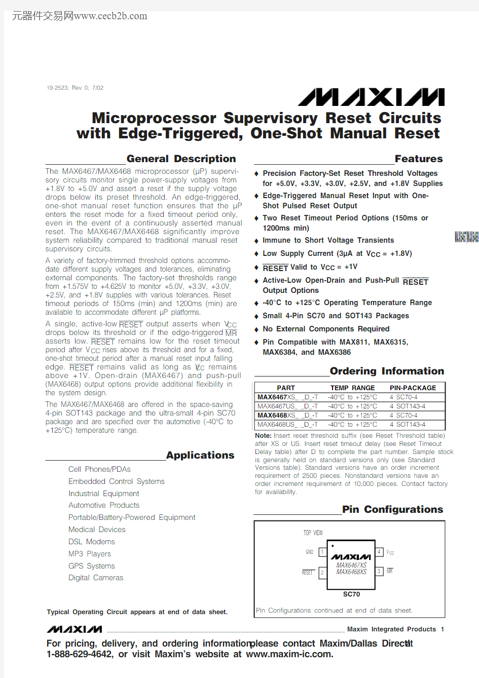
Pin Configurations
M A X 6467/M A X 6468
Microprocessor Supervisory Reset Circuits with Edge-Triggered, One-Shot Manual Reset 2_______________________________________________________________________________________
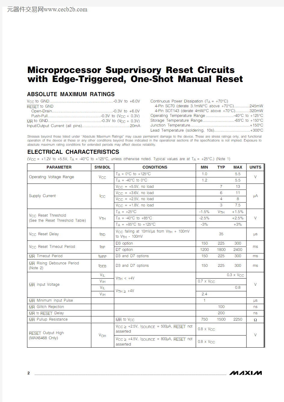
ABSOLUTE MAXIMUM RATINGS
ELECTRICAL CHARACTERISTICS
Stresses beyond those listed under “Absolute Maximum Ratings” may cause permanent damage to the device. These are stress ratings only, and functional operation of the device at these or any other conditions beyond those indicated in the operational sections of the specifications is not implied. Exposure to absolute maximum rating conditions for extended periods may affect device reliability.
V CC to GND...........................................................-0.3V to +6.0V RESET to GND
Open-Drain........................................................-0.3V to +6.0V Push-Pull.................................................-0.3V to (V CC + 0.3V)MR to GND.................................................-0.3V to (V CC + 0.3V)Input/Output Current (all pins)............................................20mA
Continuous Power Dissipation (T A = +70°C)
4-Pin SC70 (derate 3.1mW/°C above +70°C)..............245mW 4-Pin SOT143 (derate 4mW/°C above +70°C).............320mW Operating Temperature Range .........................-40°C to +125°C Storage Temperature Range.............................-65°C to +150°C Junction Temperature......................................................+150°C Lead Temperature (soldering, 10s).................................+300°C
MAX6467/MAX6468
Microprocessor Supervisory Reset Circuits with Edge-Triggered, One-Shot Manual Reset
_______________________________________________________________________________________3
ELECTRICAL CHARACTERISTICS (continued)
(V CC = +1.2V to +5.5V, T A = -40°C to +125°C, unless otherwise noted. Typical values are at T A = +25°C.) (Note 1)
Typical Operating Characteristics
(V CC = +5V, MAX6468US29D3 device, T A = +25°C, unless otherwise noted.)
SUPPLY CURRENT vs. TEMPERATURE
TEMPERATURE (°C)S U P P L Y C U R R E N T (μA )
110956580-105203550-25123456789100
-40125
SUPPLY CURRENT vs. SUPPLY VOLTAGE
M A X 6467 t o c 02
SUPPLY VOLTAGE (V)
S U P P L Y C U R R E N T (μA )
5.04.53.5 4.01.0 1.5 2.0 2.5 3.0
0.5123456789100
0 5.5
V CC TO RESET DELAY vs. TEMPERATURE
TEMPERATURE (°C)
V C C T O R E S E T D E L A Y (μs )
1109580655035205-10-2518
20
22
24
26
16
-40125
RESET TIMEOUT PERIOD vs. TEMPERATURE
M A X 6467 t o c 04
TEMPERATURE (°C)
R E S E T T I M E O U T P E R I O D (m s )
110956580-105203550-25201202203204205206207208209210200
-40125
NORMALIZED RESET THRESHOLD
vs. TEMPERATURE
M A X 6467 t o c 05
TEMPERATURE (°C)
N O R M A L I Z E D R E S E T T H R E S H O L D
(V )
1109580655035205-10-250.995
1.000
1.005
1.0100.990
-40125
OUTPUT VOLTAGE LOW vs. SINK CURRENT
I SINK (mA)
V O L (m V )
986723451501001502002503003504004505005506000
010
M A X 6467/M A X 6468
Microprocessor Supervisory Reset Circuits with Edge-Triggered, One-Shot Manual Reset 4_______________________________________________________________________________________
OUTPUT VOLTAGE HIGH vs. SOURCE CURRENT
I SOURCE (mA)V O H (V )
764
5
2
3
1
0.51.01.52.02.53.03.54.04.55.05.500
8MAXIMUM TRANSIENT DURATION vs. RESET THRESHOLD OVERDRIVE
RESET THRESHOLD OVERDRIVE (mV)
M A X I M U M T R A N S I E N T D U R A T I O N (μs )
50403020101002003004005006000
060
M A X 6467 t o c 09
TEMPERATURE (°C)
110956580-105203550-2565707580859095100105110115120
60
-40125
MR TO RESET DELAY vs. TEMPERATURE
M R T O R E S E T D E L A Y (n s )
PROPAGATION DELAY (WITH 100mV OVERDRIVE)
MAX6467 toc10
4μs/div
3.0V 3V 0
2.8V V CC 100mV/div AC-COUPLED RESET 1V/div RESET PULLUP AND PULLDOWN RESPONSE
MAX6467 toc11
40μs/div
1.675V
1.6V
1.475V
V CC 200mV/div C RESET = 47pF, R PULLUP = 100k ?,V PULLUP = 1.6V
MAX6467_S16D3-T
RESET TIMEOUT PERIOD
MAX6467 toc12
40ms/div
3.3V
3.3V 0
V CC 2V/div RESET 2V/div Typical Operating Characteristics (continued)
(V CC = +5V, MAX6468US29D3 device, T A = +25°C, unless otherwise noted.)
Detailed Description
Reset Output The MAX6467 provides an active-low open-drain RESET output. The MAX6468 provides an active-low push-pull RESET output. RESET asserts low if V CC drops below the selected threshold or if a falling edge occurs on MR. RESET remains low for the V CC reset timeout period after V CC increases above the threshold voltage or is one-shot pulsed low for the MR timeout period after a falling edge on MR.
Manual Reset Input Many μP-based products require manual reset capability, allowing the operator, a test technician, or external logic circuitry to initiate a reset. A falling edge on MR asserts RESET low. RESET is one-shot pulsed low for the MR timeout period after a falling edge on MR. An internal
1.5k?pullup resistor to V CC allows MR to be left uncon-nected if not used. MR can be driven with TTL or CMOS-
logic levels, or with open-drain/collector outputs. Connect
a normally open momentary pushbutton switch from MR
to GND to realize a manual reset function. External debounce circuitry is not required, as the MAX6467/
MAX6468 respond to the first falling edge on MR and ignore subsequent falling edges within the reset timeout period and during the MR debounce period (see Figure
1). After MR goes high for 150ms (t DEB), the manual reset
one-shot is ready to trigger a reset on the next MR falling edge. Connect a 0.1μF capacitor from MR to GND when
using long cables to provide additional noise immunity (Figure 2).
MAX6467/MAX6468
Microprocessor Supervisory Reset Circuits with Edge-Triggered, One-Shot Manual Reset
_______________________________________________________________________________________5
M A X 6467/M A X 6468
Applications Information
Falling V CC Transients
In addition to issuing a reset to the μP during power-up,power-down, and brownout conditions, the MAX6467/MAX6468 are relatively immune to short-duration falling V CC transients (glitches). The Typical Operating Characteristics section shows the Maximum Transient Duration vs. V CC Overdrive for which the MAX6467/MAX6468 do not generate a reset pulse. This graph was generated using a falling pulse applied to V CC starting above the actual reset threshold and ending below the threshold by the magnitude indicated (V CC Overdrive).The graph indicates the typical maximum pulse width a falling V CC transient can have without initiating a reset pulse. As the magnitude of the transient increases (goes
farther below the reset threshold), the maximum allowable pulse width decreases. A 0.1μF bypass capacitor from V CC to GND provides additional transient immunity.
Ensuring a Valid RESET Output Down
to V CC = 0V
The MAX6467/MAX6468 guarantee proper operation down to V CC = +1V. I n applications that require valid reset levels down to V CC = 0V, a pulldown resistor to active-low outputs (MAX6468 only, Figure 3) ensures that RESET remains valid while the RESET output can no longer sink current. This scheme does not work with the open-drain outputs of the MAX6467. Ensure that the resistor value used does not overload the RESET output when V CC is above the reset threshold. For most appli-cations, use 100k ?to 1M ?.
Microprocessor Supervisory Reset Circuits with Edge-Triggered, One-Shot Manual Reset 6_______________________________________________________________________________________
Figure 3. RESET Valid to V CC = 0V
Chip Information
TRANSISTOR COUNT: 748PROCESS: BiCMOS
Figure 2. Functional Diagram
MAX6467/MAX6468
Microprocessor Supervisory Reset Circuits with Edge-Triggered, One-Shot Manual Reset
_______________________________________________________________________________________7
Typical Operating Circuit
Reset Threshold (-40°C to +85°C)
Pin Configurations (continued)
Standard Versions
M A X 6467/M A X 6468
Microprocessor Supervisory Reset Circuits with Edge-Triggered, One-Shot Manual Reset 8
_______________________________________________________________________________________
Package Information
(The package drawing(s) in this data sheet may not reflect the most current specifications. For the latest package outline information,go to https://www.360docs.net/doc/ec2628721.html,/packages .)
MAX6467/MAX6468
Microprocessor Supervisory Reset Circuits with Edge-Triggered, One-Shot Manual Reset
Maxim cannot assume responsibility for use of any circuitry other than circuitry entirely embodied in a Maxim product. No circuit patent licenses are implied. Maxim reserves the right to change the circuitry and specifications without notice at any time.
Maxim Integrated Products, 120 San Gabriel Drive, Sunnyvale, CA 94086 408-737-7600 _____________________9?2002 Maxim Integrated Products
Printed USA
is a registered trademark of Maxim Integrated Products.
Package Information (continued)
(The package drawing(s) in this data sheet may not reflect the most current specifications. For the latest package outline information,go to https://www.360docs.net/doc/ec2628721.html,/packages
.)
S C 70, 4L .E P S