SN74AVC2T45DCTTE4中文资料
https://www.360docs.net/doc/e34417040.html,
FEATURES
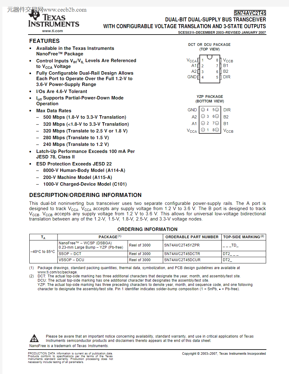
DCT OR DCU PACKAGE
(TOP VIEW)
1
2
3
4
8
7
6
5
V CCA
A1
A2
GND
V CCB
B1
B2
DIR
YZP PACKAGE
(BOTTOM VIEW)
GND
A2
A1
V CCA
DIR
B2
B1
V CCB DESCRIPTION/ORDERING INFORMATION
SN74AVC2T45
DUAL-BIT DUAL-SUPPLY BUS TRANSCEIVER
WITH CONFIGURABLE VOLTAGE TRANSLATION AND3-STATE OUTPUTS
SCES531I–DECEMBER2003–REVISED JANUARY2007
?Available in the Texas Instruments
NanoFree?Package
?Control Inputs V IH/V IL Levels Are Referenced
to V CCA Voltage
?Fully Configurable Dual-Rail Design Allows
Each Port to Operate Over the Full1.2-V to
3.6-V Power-Supply Range
?I/Os Are4.6-V Tolerant
?I off Supports Partial-Power-Down Mode
Operation
?Max Data Rates
–500Mbps(1.8-V to3.3-V Translation)
–320Mbps(<1.8-V to3.3-V Translation)
–320Mbps(Translate to2.5V or1.8V)
–280Mbps(Translate to1.5V)
–240Mbps(Translate to1.2V)
?Latch-Up Performance Exceeds100mA Per
JESD78,Class II
?ESD Protection Exceeds JESD22
–8000-V Human-Body Model(A114-A)
–200-V Machine Model(A115-A)
–1000-V Charged-Device Model(C101)
This dual-bit noninverting bus transceiver uses two separate configurable power-supply rails.The A port is designed to track V CCA.V CCA accepts any supply voltage from1.2V to3.6V.The B port is designed to track V CCB.V CCB accepts any supply voltage from1.2V to3.6V.This allows for universal low-voltage bidirectional translation between any of the1.2-V,1.5-V,1.8-V,2.5-V,and3.3-V voltage nodes.
ORDERING INFORMATION
T A PACKAGE(1)ORDERABLE PART NUMBER TOP-SIDE MARKING(2)
NanoFree?–WCSP(DSBGA)
Reel of3000SN74AVC2T45YZPR___TD_
0.23-mm Large Bump–YZP(Pb-free)
–40°C to85°C
SSOP–DCT Reel of3000SN74AVC2T45DCTR DT2___
VSSOP–DCU Reel of3000SN74AVC2T45DCUR DT2_
(1)Package drawings,standard packing quantities,thermal data,symbolization,and PCB design guidelines are available at
https://www.360docs.net/doc/e34417040.html,/sc/package.
(2)DCT:The actual top-side marking has three additional characters that designate the year,month,and assembly/test site.
DCU:The actual top-side marking has one additional character that designates the assembly/test site.
YZP:The actual top-side marking has three preceding characters to denote year,month,and sequence code,and one following
character to designate the assembly/test site.Pin1identifier indicates solder-bump composition(1=SnPb,?=Pb-free).
Please be aware that an important notice concerning availability,standard warranty,and use in critical applications of Texas
Instruments semiconductor products and disclaimers thereto appears at the end of this data sheet.
NanoFree is a trademark of Texas Instruments.
PRODUCTION DATA information is current as of publication date.Copyright?2003–2007,Texas Instruments Incorporated Products conform to specifications per the terms of the Texas
Instruments standard warranty.Production processing does not
necessarily include testing of all parameters.
元器件交易网https://www.360docs.net/doc/e34417040.html,
https://www.360docs.net/doc/e34417040.html,
DESCRIPTION/ORDERING INFORMATION (CONTINUED)
B1
DIR
A1
V CCA V CCB
B2
A2
SN74AVC2T45
DUAL-BIT DUAL-SUPPLY BUS TRANSCEIVER
WITH CONFIGURABLE VOLTAGE TRANSLATION AND 3-STATE OUTPUTS
SCES531I–DECEMBER 2003–REVISED JANUARY 2007
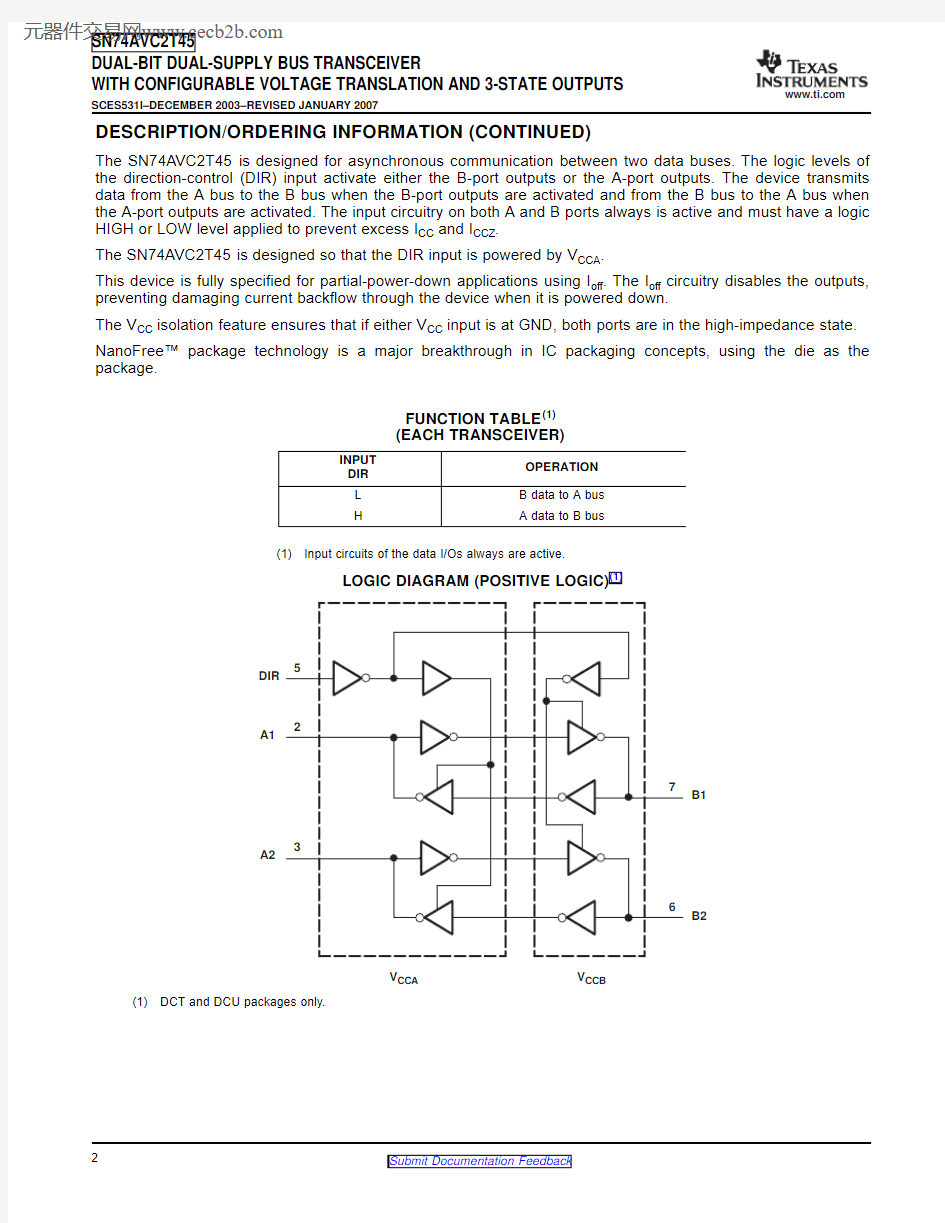
The SN74AVC2T45is designed for asynchronous communication between two data buses.The logic levels of the direction-control (DIR)input activate either the B-port outputs or the A-port outputs.The device transmits data from the A bus to the B bus when the B-port outputs are activated and from the B bus to the A bus when the A-port outputs are activated.The input circuitry on both A and B ports always is active and must have a logic HIGH or LOW level applied to prevent excess I CC and I CCZ .
The SN74AVC2T45is designed so that the DIR input is powered by V CCA .
This device is fully specified for partial-power-down applications using I off .The I off circuitry disables the outputs,preventing damaging current backflow through the device when it is powered down.
The V CC isolation feature ensures that if either V CC input is at GND,both ports are in the high-impedance state.NanoFree?package technology is a major breakthrough in IC packaging concepts,using the die as the package.
FUNCTION TABLE (1)(EACH TRANSCEIVER)
INPUT OPERATION DIR L B data to A bus H
A data to
B bus
(1)
Input circuits of the data I/Os always are active.
LOGIC DIAGRAM (POSITIVE LOGIC)(1)
(1)DCT and DCU packages only.
2
Submit Documentation Feedback
元器件交易网https://www.360docs.net/doc/e34417040.html,
https://www.360docs.net/doc/e34417040.html,
Absolute Maximum Ratings(1)
SN74AVC2T45
DUAL-BIT DUAL-SUPPLY BUS TRANSCEIVER WITH CONFIGURABLE VOLTAGE TRANSLATION AND3-STATE OUTPUTS
SCES531I–DECEMBER2003–REVISED JANUARY2007
over operating free-air temperature range(unless otherwise noted)
MIN MAX UNIT
V CCA
Supply voltage range–0.5 4.6V V CCB
I/O ports(A port)–0.5 4.6
V I Input voltage range(2)I/O ports(B port)–0.5 4.6V
Control inputs–0.5 4.6
A port–0.5 4.6
Voltage range applied to any output in the high-impedance or
V O V power-off state(2)B port–0.5 4.6
A port–0.5V CCA+0.5
V O Voltage range applied to any output in the high or low state(2)(3)V
B port–0.5V CCB+0.5
I IK Input clamp current V I<0–50mA
I OK Output clamp current V O<0–50mA
I O Continuous output current±50mA
Continuous current through V CCA,V CCB,or GND±100mA
DCT package220
θJA Package thermal impedance(4)DCU package227°C/W
YZP package102
T stg Storage temperature range–65150°C
(1)Stresses beyond those listed under"absolute maximum ratings"may cause permanent damage to the device.These are stress ratings
only,and functional operation of the device at these or any other conditions beyond those indicated under"recommended operating
conditions"is not implied.Exposure to absolute-maximum-rated conditions for extended periods may affect device reliability.
(2)The input negative-voltage and output voltage ratings may be exceeded if the input and output current ratings are observed.
(3)The output positive-voltage rating may be exceeded up to4.6V maximum if the output current ratings are observed.
(4)The package thermal impedance is calculated in accordance with JESD51-7.
3
Submit Documentation Feedback
元器件交易网https://www.360docs.net/doc/e34417040.html,
https://www.360docs.net/doc/e34417040.html,
Recommended Operating Conditions (1)(2)(3)(4)(5)
SN74AVC2T45
DUAL-BIT DUAL-SUPPLY BUS TRANSCEIVER
WITH CONFIGURABLE VOLTAGE TRANSLATION AND 3-STATE OUTPUTS
SCES531I–DECEMBER 2003–REVISED JANUARY 2007
V CCI
V CCO
MIN MAX UNIT V CCA Supply voltage 1.2 3.6V V CCB Supply voltage
1.2
3.6
V
1.2V to 1.95V
V CCI ×0.65
High-level V IH
Data inputs (4)
1.95V to
2.7V 1.6V
input voltage
2.7V to
3.6V 2
1.2V to 1.95V
V CCI ×0.35
Low-level V IL
Data inputs (4)
1.95V to
2.7V 0.7V input voltage
2.7V to
3.6V 0.8
1.2V to 1.95V
V CCA ×0.65
High-level DIR
V IH
1.95V to
2.7V 1.6V
input voltage
(referenced to V CCA )(5)
2.7V to
3.6V 2
1.2V to 1.95V
V CCA ×0.35
Low-level DIR
V IL 1.95V to 2.7V 0.7V input voltage (referenced to V CCA )(5)
2.7V to
3.6V
0.8V I Input voltage 0 3.6V Active state 0V CCO V O
Output voltage
V 3-state
3.61.2V –31.4V to 1.6V
–6I OH
High-level output current
1.65V to 1.95V –8mA
2.3V to 2.7V –93V to
3.6V –121.2V 31.4V to 1.6V
6I OL
Low-level output current
1.65V to 1.95V 8mA
2.3V to 2.7V 93V to
3.6V
12?t/?v Input transition rise or fall rate 5ns/V T A Operating free-air temperature
–40
85
°C (1)V CCI is the V CC associated with the input port.(2)V CCO is the V CC associated with the output port.
(3)All unused data inputs of the device must be held at V CCI or GND to ensure proper device operation.Refer to the TI application report,Implications of Slow or Floating CMOS Inputs ,literature number SCBA004.
(4)For V CCI values not specified in the data sheet,V IH min =V CCI ×0.7V,V IL max =V CCI ×0.3V.(5)
For V CCI values not specified in the data sheet,V IH min =V CCA ×0.7V,V IL max =V CCA ×0.3V.
4
Submit Documentation Feedback
元器件交易网https://www.360docs.net/doc/e34417040.html,
https://www.360docs.net/doc/e34417040.html,
Electrical Characteristics(1)(2)
SN74AVC2T45
DUAL-BIT DUAL-SUPPLY BUS TRANSCEIVER WITH CONFIGURABLE VOLTAGE TRANSLATION AND3-STATE OUTPUTS
SCES531I–DECEMBER2003–REVISED JANUARY2007
over recommended operating free-air temperature range(unless otherwise noted)
T A=25°C–40°C to85°C PARAMETER TEST CONDITIONS V CCA V CCB UNIT
MIN TYP MAX MIN MAX
I OH=–100μA 1.2V to3.6V 1.2V to3.6V V CCO–0.2V
I OH=–3mA 1.2V 1.2V0.95
I OH=–6mA 1.4V 1.4V 1.05
V OH V I=V IH V
I OH=–8mA 1.65V 1.65V 1.2
I OH=–9mA 2.3V 2.3V 1.75
I OH=–12mA3V3V 2.3
I OL=100μA 1.2V to3.6V 1.2V to3.6V0.2
I OL=3mA 1.2V 1.2V0.25
I OL=6mA 1.4V 1.4V0.35
V OL V I=V IL V
I OL=8mA 1.65V 1.65V0.45
I OL=9mA 2.3V 2.3V0.55
I OL=12mA3V3V0.7
I I DIR V I=V CCA or GND 1.2V to3.6V 1.2V to3.6V±0.025±0.25±1μA
A port0V0to3.6V±0.1±1±5
I off V I or V O=0to3.6VμA
B port0to3.6V0V±0.1±1±5
A or B
I OZ V O=V CCO or GND 1.2V to3.6V 1.2V to3.6V±0.5±2.5±5μA
port
1.2V to3.6V 1.2V to3.6V10
I CCA V I=V CCI or GND,I O=00V 3.6V–2μA
3.6V0V10
1.2V to3.6V 1.2V to3.6V10
I CCB V I=V CCI or GND,I O=00V 3.6V10μA
3.6V0V–2
I CCA+I CCB
V I=V CCI or GND,I O=0 1.2V to3.6V 1.2V to3.6V20μA (see Table1)
Control
C I V I=3.3V or GN
D 3.3V 3.3V 2.5pF
inputs
A or B
C io V O=3.3V or GN
D 3.3V 3.3V6pF
port
(1)V CCO is the V CC associated with the output port.
(2)V CCI is the V CC associated with the input port.
5
Submit Documentation Feedback
元器件交易网https://www.360docs.net/doc/e34417040.html,
https://www.360docs.net/doc/e34417040.html,
Switching Characteristics
Switching Characteristics
SN74AVC2T45
DUAL-BIT DUAL-SUPPLY BUS TRANSCEIVER
WITH CONFIGURABLE VOLTAGE TRANSLATION AND 3-STATE OUTPUTS
SCES531I–DECEMBER 2003–REVISED JANUARY 2007
over recommended operating free-air temperature range,V CCA =1.2V (see Figure 1)
V CCB =1.2V
V CCB =1.5V
V CCB =1.8V
V CCB =2.5V
V CCB =3.3V
FROM TO PARAMETER
UNIT (INPUT)(OUTPUT)
TYP TYP TYP TYP TYP t PLH 3.1 2.6 2.4 2.2 2.2A B ns t PHL 3.1 2.6 2.4 2.2 2.2t PLH 3.4 3.13 2.9 2.9B A ns t PHL 3.4 3.13 2.9 2.9t PHZ 5.2 5.2 5.15 4.8DIR A ns t PLZ 5.2 5.2 5.15 4.8t PHZ 54 3.8 2.8 3.2DIR B ns t PLZ 54 3.8 2.8 3.2t PZH (1)8.47.1 6.8 5.7 6.1DIR A ns t PZL (1)8.47.1 6.8 5.7 6.1t PZH (1)8.37.87.57.27DIR
B
ns
t PZL (1)
8.3
7.8
7.5
7.2
7
(1)
The enable time is a calculated value,derived using the formula shown in the enable times section.
over recommended operating free-air temperature range,V CCA =1.5V ±0.1V (see Figure 1)
V CCB =1.5V V CCB =1.8V V CCB =2.5V V CCB =3.3V V CCB =1.2V
FROM TO ±0.1V ±0.15V ±0.2V ±0.3V PARAMETER
UNIT
(INPUT)(OUTPUT)
TYP MIN MAX MIN MAX MIN MAX MIN MAX t PLH 2.80.7 5.40.5 4.60.4 3.70.3 3.5A B ns t PHL 2.80.7 5.40.5 4.60.4 3.70.3 3.5t PLH 2.70.8 5.40.7 5.20.6 4.90.5 4.7B A ns t PHL 2.70.8 5.40.7 5.20.6 4.90.5 4.7t PHZ 3.9 1.38.5 1.37.8 1.17.7 1.47.6DIR A ns t PLZ 3.9 1.38.5 1.37.8 1.17.7 1.47.6t PHZ 4.7 1.17 1.4 6.9 1.2 6.9 1.77.1DIR B ns t PLZ 4.7 1.1
7 1.4
6.9 1.2
6.9 1.7
7.1t PZH (1)7.412.412.111.811.8DIR A ns t PZL (1)7.412.412.111.811.8t PZH (1) 6.713.911.69.17.8DIR
B
ns t PZL (1)
6.7
13.9
11.6
9.1
7.8
(1)
The enable time is a calculated value,derived using the formula shown in the enable times section.
6
Submit Documentation Feedback
元器件交易网https://www.360docs.net/doc/e34417040.html,
https://www.360docs.net/doc/e34417040.html,
Switching Characteristics Switching Characteristics
SN74AVC2T45
DUAL-BIT DUAL-SUPPLY BUS TRANSCEIVER WITH CONFIGURABLE VOLTAGE TRANSLATION AND3-STATE OUTPUTS
SCES531I–DECEMBER2003–REVISED JANUARY2007
over recommended operating free-air temperature range,V
CCA
=1.8V±0.15V(see Figure1)
V CCB=1.5V V CCB=1.8V V CCB=2.5V V CCB=3.3V
V CCB=1.2V
FROM TO±0.1V±0.15V±0.2V±0.3V PARAMETER UNIT (INPUT)(OUTPUT)
TYP MIN MAX MIN MAX MIN MAX MIN MAX
t PLH 2.70.5 5.20.4 4.30.2 3.40.2 3.1
A B ns
t PHL 2.70.5 5.20.4 4.30.2 3.40.2 3.1
t PLH 2.40.7 4.70.5 4.40.540.4 3.8
B A ns
t PHL 2.40.7 4.70.5 4.40.540.4 3.8
t PHZ 3.7 1.38.10.7 6.9 1.4 5.3 1.1 5.2
DIR A ns t PLZ 3.7 1.38.10.7 6.9 1.4 5.3 1.1 5.2
t PHZ 4.4 1.3 5.8 1.3 5.90.8 5.7 1.5 5.9
DIR B ns t PLZ 4.4 1.3 5.8 1.3 5.90.8 5.7 1.5 5.9
t PZH(1) 6.810.410.39.79.7
DIR A ns t PZL(1) 6.810.410.39.79.7
t PZH(1) 6.413.311.28.68.3
DIR B ns t PZL(1) 6.413.311.28.68.3
(1)The enable time is a calculated value,derived using the formula shown in the enable times section.
over recommended operating free-air temperature range,V
CCA
=2.5V±0.2V(see Figure1)
V CCB=1.5V V CCB=1.8V V CCB=2.5V V CCB=3.3V
V CCB=1.2V
FROM TO±0.1V±0.15V±0.2V±0.3V PARAMETER UNIT (INPUT)(OUTPUT)
TYP MIN MAX MIN MAX MIN MAX MIN MAX
t PLH 2.60.4 4.90.240.230.2 2.6
A B ns
t PHL 2.60.4 4.90.240.230.2 2.6
t PLH 2.10.6 3.80.5 3.40.430.3 2.8
B A ns
t PHL 2.10.6 3.80.5 3.40.430.3 2.8
t PHZ 2.40.77.90.8 6.40.850.5 4.3
DIR A ns t PLZ 2.40.77.90.8 6.40.850.5 4.3
t PHZ 3.81 4.30.6 4.30.5 4.2 1.1 4.1
DIR B ns t PLZ 3.81 4.30.6 4.30.5 4.2 1.1 4.1
t PZH(1) 5.97.97.77.2 6.9
DIR A ns t PZL(1) 5.97.97.77.2 6.9
t PZH(1)512.810.47.9 6.8
DIR B ns t PZL(1)512.810.47.9 6.8
(1)The enable time is a calculated value,derived using the formula shown in the enable times section.
7
Submit Documentation Feedback
元器件交易网https://www.360docs.net/doc/e34417040.html,
https://www.360docs.net/doc/e34417040.html,
Switching Characteristics
Operating Characteristics
SN74AVC2T45
DUAL-BIT DUAL-SUPPLY BUS TRANSCEIVER
WITH CONFIGURABLE VOLTAGE TRANSLATION AND 3-STATE OUTPUTS
SCES531I–DECEMBER 2003–REVISED JANUARY 2007
over recommended operating free-air temperature range,V CCA =3.3V ±0.3V (see Figure 1)
V CCB =1.5V V CCB =1.8V V CCB =2.5V V CCB =3.3V V CCB =1.2V
FROM TO ±0.1V ±0.15V ±0.2V ±0.3V PARAMETER
UNIT
(INPUT)(OUTPUT)
TYP MIN MAX MIN MAX MIN MAX MIN MAX t PLH 2.50.3 4.70.2 3.80.2 2.80.2 2.4A B ns t PHL 2.50.3 4.70.2 3.80.2 2.80.2 2.4t PLH 2.10.6 3.60.4 3.10.3 2.60.3 2.4B A ns t PHL 2.10.6 3.60.4 3.10.3 2.60.3 2.4t PHZ 2.9 1.181 6.5 1.3 4.7 1.24DIR A ns t PLZ 2.9 1.181 6.5 1.3 4.7 1.24t PHZ 3.40.5 6.60.3 5.60.3 4.6 1.1 4.2DIR B ns t PLZ 3.40.5
6.60.3
5.60.3
4.6 1.1
4.2t PZH (1)
5.5
6.9 6.6 6.2 6.6DIR A ns t PZL (1) 5.5 6.9 6.6 6.2 6.6t PZH (1) 5.412.710.3
7.4 6.3DIR
B
ns t PZL (1)
5.4
12.7
10.3
7.4
6.3
(1)
The enable time is a calculated value,derived using the formula shown in the enable times section.
T A =25°C
V CCA =V CCA =V CCA =V CCA =V CCA =TEST V CCB =1.2V
V CCB =1.5V
V CCB =1.8V
V CCB =2.5V
V CCB =3.3V
PARAMETER UNIT
CONDITIONS TYP TYP TYP TYP TYP A-port input,33334
C L =0,B-port output C pdA
(1)
f =10MHz,pF
B-port input,t r =t f =1ns 1213131415A-port output
A-port input,1213131415
C L =0,B-port output C pdB
(1)
f =10MHz,pF
B-port input,t r =t f =1ns
3
3
3
3
4
A-port output
(1)Power-dissipation capacitance per transceiver
8
Submit Documentation Feedback
元器件交易网https://www.360docs.net/doc/e34417040.html,
https://www.360docs.net/doc/e34417040.html,
Power-Up Considerations SN74AVC2T45
DUAL-BIT DUAL-SUPPLY BUS TRANSCEIVER
WITH CONFIGURABLE VOLTAGE TRANSLATION AND3-STATE OUTPUTS
SCES531I–DECEMBER2003–REVISED JANUARY2007
A proper power-up sequence always should be followed to avoid excessive supply current,bus contention,
oscillations,or other anomalies.To guard against such power-up problems,take the following precautions:
1.Connect ground before any supply voltage is applied.
2.Power up V CCA.
3.V CCB can be ramped up along with or after V CCA.
Table1.Typical Total Static Power Consumption(I CCA+I CCB)
V CCA
V CCB UNIT
0V 1.2V 1.5V 1.8V 2.5V 3.3V
0V0<0.5<0.5<0.5<0.5<0.5
1.2V<0.5<1<1<1<11
1.5V<0.5<1<1<1<11
μA
1.8V<0.5<1<1<1<1<1
2.5V<0.51<1<1<1<1
3.3V<0.51<1<1<1<1
9
Submit Documentation Feedback
元器件交易网https://www.360docs.net/doc/e34417040.html,
https://www.360docs.net/doc/e34417040.html,
TYPICAL CHARACTERISTICS
TYPICAL PROPAGATION DELAY (A to B)vs LOAD CAPACITANCE,
t P H L - n s
C L - pF
t P L H - n s
C L - pF
TYPICAL PROPAGATION DELAY (A to B)vs LOAD CAPACITANCE,
t P H L - n s
C
L - pF
01020
30405060
t P L H - n s
C L - pF
SN74AVC2T45
DUAL-BIT DUAL-SUPPLY BUS TRANSCEIVER
WITH CONFIGURABLE VOLTAGE TRANSLATION AND 3-STATE OUTPUTS
SCES531I–DECEMBER 2003–REVISED JANUARY 2007
T A =25°C,V CCA =1.2V
T A =25°C,V CCA =1.5V
10
Submit Documentation Feedback
元器件交易网https://www.360docs.net/doc/e34417040.html,
https://www.360docs.net/doc/e34417040.html,
TYPICAL CHARACTERISTICS
TYPICAL PROPAGATION DELAY (A to B)vs LOAD CAPACITANCE,
t P H L - n s
C L - pF
t P L H - n s
C L - pF
TYPICAL PROPAGATION DELAY (A to B)vs LOAD CAPACITANCE,
t P H L - n s
C
L - pF
01020
30405060
t P L H - n s
C L - pF
SN74AVC2T45
DUAL-BIT DUAL-SUPPLY BUS TRANSCEIVER
WITH CONFIGURABLE VOLTAGE TRANSLATION AND 3-STATE OUTPUTS
SCES531I–DECEMBER 2003–REVISED JANUARY 2007
T A =25°C,V CCA =1.8V
T A =25°C,V CCA =2.5V
11
Submit Documentation Feedback
元器件交易网https://www.360docs.net/doc/e34417040.html,
https://www.360docs.net/doc/e34417040.html,
TYPICAL CHARACTERISTICS
TYPICAL PROPAGATION DELAY (A to B)vs LOAD CAPACITANCE,
t P H L - n s
C L - pF
t P L H - n s
C L - pF
SN74AVC2T45
DUAL-BIT DUAL-SUPPLY BUS TRANSCEIVER
WITH CONFIGURABLE VOLTAGE TRANSLATION AND 3-STATE OUTPUTS
SCES531I–DECEMBER 2003–REVISED JANUARY 2007
T A =25°C,V CCA =3.3V
12
Submit Documentation Feedback
元器件交易网https://www.360docs.net/doc/e34417040.html,
https://www.360docs.net/doc/e34417040.html,
PARAMETER MEASUREMENT INFORMATION
V OH V OL
LOAD CIRCUIT × V CCO
Open
Output Control (low-level enabling)
Output Waveform 1S1 at 2 × V CCO (see Note B)Output Waveform 2S1 at GND (see Note B)
0 V
0 V
V CCI
0 V
V CCA
V CCO
VOLTAGE WAVEFORMS PROPAGATION DELAY TIMES
VOLTAGE WAVEFORMS PULSE DURATION
VOLTAGE WAVEFORMS ENABLE AND DISABLE TIMES
Input
t pd t PLZ /t PZL t PHZ /t PZH
Open 2 × V CCO GND
TEST S1NOTES: A.C L includes probe and jig capacitance.
B.Waveform 1 is for an output with internal conditions such that the output is low, except when disabled by the output control.
Waveform 2 is for an output with internal conditions such that the output is high, except when disabled by the output control.C.All input pulses are supplied by generators having the following characteristics: PRR v 10 MHz, Z O = 50 ?, dv/dt ≥ 1 V/ns.D.The outputs are measured one at a time, with one transition per measurement.E.t PLZ and t PHZ are the same as t dis .F.t PZL and t PZH are the same as t en .G.t PLH and t PHL are the same as t pd .
H.V CCI is the V CC associated with the input port.I.V CCO is the V CC associated with the output port.
1.2 V 1.5 V ± 0.1 V 1.8 V ± 0.15 V
2.5 V ± 0.2 V
3.3 V ± 0.3 V
2 k ?2 k ?2 k ?2 k ?2 k ?
V CCO R L 0.1 V 0.1 V 0.15 V 0.15 V 0.3 V
V TP C L 15 pF 15 pF 15 pF 15 pF 15 pF
SN74AVC2T45
DUAL-BIT DUAL-SUPPLY BUS TRANSCEIVER
WITH CONFIGURABLE VOLTAGE TRANSLATION AND 3-STATE OUTPUTS
SCES531I–DECEMBER 2003–REVISED JANUARY 2007
Figure 1.Load Circuit and Voltage Waveforms
13
Submit Documentation Feedback
元器件交易网https://www.360docs.net/doc/e34417040.html,
https://www.360docs.net/doc/e34417040.html,
APPLICATION INFORMATION
SYSTEM-1SYSTEM-2
SN74AVC2T45
DUAL-BIT DUAL-SUPPLY BUS TRANSCEIVER
WITH CONFIGURABLE VOLTAGE TRANSLATION AND 3-STATE OUTPUTS
SCES531I–DECEMBER 2003–REVISED JANUARY 2007
Figure 2is an example circuit of the SN74AVC2T45used in a unidirectional logic level-shifting application.
PIN NAME FUNCTION DESCRIPTION
1V CCA V CC1SYSTEM-1supply voltage (1.2V to 3.6V)2A1OUT1Output level depends on V CC1voltage.3A2OUT2Output level depends on V CC1voltage.4GND GND Device GND
5DIR DIR The GND (low-level)determines B-port to A-port direction.6B2IN2Input threshold value depends on V CC2voltage.7B1IN1Input threshold value depends on V CC2voltage.8
V CCB
V CC2
SYSTEM-2supply voltage (1.2V to 3.6V)
Figure 2.Unidirectional Logic Level-Shifting Application
14
Submit Documentation Feedback
元器件交易网https://www.360docs.net/doc/e34417040.html,
https://www.360docs.net/doc/e34417040.html,
APPLICATION INFORMATION
SYSTEM-1SYSTEM-2
Enable Times
SN74AVC2T45
DUAL-BIT DUAL-SUPPLY BUS TRANSCEIVER
WITH CONFIGURABLE VOLTAGE TRANSLATION AND 3-STATE OUTPUTS
SCES531I–DECEMBER 2003–REVISED JANUARY 2007
Figure 3shows the SN74AVC2T45used in a bidirectional logic level-shifting application.Since the does not have an output-enable (OE)pin,the system designer should take precautions to avoid bus contention between SYSTEM-1and SYSTEM-2when changing directions.
Following is a sequence that illustrates data transmission from SYSTEM-1to SYSTEM-2and then from SYSTEM-2to SYSTEM-1.
STATE DIR CTRL
I/O-1I/O-2DESCRIPTION
1H Out In SYSTEM-1data to SYSTEM-2
SYSTEM-2is getting ready to send data to SYSTEM-1.I/O-1and I/O-2are 2H Hi-Z Hi-Z disabled.
The bus-line state depends on pullup or pulldown.(1)DIR bit is flipped.I/O-1and I/O-2still are disabled.3L Hi-Z Hi-Z The bus-line state depends on pullup or pulldown.(1)4L
Out
In
SYSTEM-2data to SYSTEM-1
(1)
SYSTEM-1and SYSTEM-2must use the same conditions,i.e.,both pullup or both pulldown.
Figure 3.Bidirectional Logic Level-Shifting Application
Calculate the enable times for the SN74AVC2T45using the following formulas:?t PZH (DIR to A)=t PLZ (DIR to B)+t PLH (B to A)?t PZL (DIR to A)=t PHZ (DIR to B)+t PHL (B to A)?t PZH (DIR to B)=t PLZ (DIR to A)+t PLH (A to B)?t PZL (DIR to B)=t PHZ (DIR to A)+t PHL (A to B)
In a bidirectional application,these enable times provide the maximum delay from the time the DIR bit is switched until an output is expected.For example,if the SN74AVC2T45initially is transmitting from A to B,then the DIR bit is switched;the B port of the device must be disabled before presenting it with an input.After the B port has been disabled,an input signal applied to it appears on the corresponding A port after the specified propagation delay.
15
Submit Documentation Feedback
元器件交易网https://www.360docs.net/doc/e34417040.html,
PACKAGING INFORMATION
Orderable Device Status (1)Package Type Package Drawing Pins Package Qty Eco Plan (2)
Lead/Ball Finish MSL Peak Temp (3)SN74AVC2T45DCTR ACTIVE SM8DCT 83000Pb-Free (RoHS)CU NIPDAU Level-1-260C-UNLIM SN74AVC2T45DCTRE4ACTIVE SM8DCT 83000Pb-Free (RoHS)CU NIPDAU Level-1-260C-UNLIM SN74AVC2T45DCTT ACTIVE SM8DCT 8250Pb-Free (RoHS)CU NIPDAU Level-1-260C-UNLIM SN74AVC2T45DCTTE4ACTIVE SM8DCT 8250
Pb-Free (RoHS)
CU NIPDAU Level-1-260C-UNLIM SN74AVC2T45DCUR ACTIVE US8DCU 83000Green (RoHS &
no Sb/Br)CU NIPDAU Level-1-260C-UNLIM SN74AVC2T45DCURE4ACTIVE US8DCU 83000Green (RoHS &
no Sb/Br)CU NIPDAU Level-1-260C-UNLIM SN74AVC2T45DCUT ACTIVE US8DCU 8250Green (RoHS &no Sb/Br)CU NIPDAU Level-1-260C-UNLIM SN74AVC2T45DCUTE4ACTIVE US8DCU 8250
Green (RoHS &no Sb/Br)
CU NIPDAU Level-1-260C-UNLIM SN74AVC2T45YZPR
ACTIVE
WCSP
YZP
8
3000Green (RoHS &
no Sb/Br)
SNAGCU
Level-1-260C-UNLIM
(1)
The marketing status values are defined as follows:ACTIVE:Product device recommended for new designs.
LIFEBUY:TI has announced that the device will be discontinued,and a lifetime-buy period is in effect.
NRND:Not recommended for new designs.Device is in production to support existing customers,but TI does not recommend using this part in a new design.
PREVIEW:Device has been announced but is not in production.Samples may or may not be available.OBSOLETE:TI has discontinued the production of the device.
(2)
Eco Plan -The planned eco-friendly classification:Pb-Free (RoHS),Pb-Free (RoHS Exempt),or Green (RoHS &no Sb/Br)-please check https://www.360docs.net/doc/e34417040.html,/productcontent for the latest availability information and additional product content details.TBD:The Pb-Free/Green conversion plan has not been defined.
Pb-Free (RoHS):TI's terms "Lead-Free"or "Pb-Free"mean semiconductor products that are compatible with the current RoHS requirements for all 6substances,including the requirement that lead not exceed 0.1%by weight in homogeneous materials.Where designed to be soldered at high temperatures,TI Pb-Free products are suitable for use in specified lead-free processes.
Pb-Free (RoHS Exempt):This component has a RoHS exemption for either 1)lead-based flip-chip solder bumps used between the die and package,or 2)lead-based die
adhesive used between the die and leadframe.The component is otherwise considered Pb-Free (RoHS compatible)as defined above.
Green (RoHS &no Sb/Br):TI defines "Green"to mean Pb-Free (RoHS compatible),and free of Bromine (Br)and Antimony (Sb)based flame retardants (Br or Sb do not exceed 0.1%by weight in homogeneous material)
(3)
MSL,Peak Temp.--The Moisture Sensitivity Level rating according to the JEDEC industry standard classifications,and peak solder temperature.
Important Information and Disclaimer:The information provided on this page represents TI's knowledge and belief as of the date that it is provided.TI bases its knowledge and belief on information provided by third parties,and makes no representation or warranty as to the accuracy of such information.Efforts are underway to better integrate information from third parties.TI has taken and continues to take reasonable steps to provide representative and accurate information but may not have conducted destructive testing or chemical analysis on incoming materials and chemicals.TI and TI suppliers consider certain information to be proprietary,and thus CAS numbers and other limited information may not be available for release.
In no event shall TI's liability arising out of such information exceed the total purchase price of the TI part(s)at issue in this document sold by TI to Customer on an annual basis.
PACKAGE OPTION ADDENDUM
https://www.360docs.net/doc/e34417040.html,
18-Jan-2007
Addendum-Page 1
元器件交易网https://www.360docs.net/doc/e34417040.html,
IMPORTANT NOTICE
Texas Instruments Incorporated and its subsidiaries (TI) reserve the right to make corrections, modifications, enhancements, improvements, and other changes to its products and services at any time and to
discontinue any product or service without notice. Customers should obtain the latest relevant information
before placing orders and should verify that such information is current and complete. All products are sold
subject to TI’s terms and conditions of sale supplied at the time of order acknowledgment.
TI warrants performance of its hardware products to the specifications applicable at the time of sale in
accordance with TI’s standard warranty. Testing and other quality control techniques are used to the extent
TI deems necessary to support this warranty. Except where mandated by government requirements, testing
of all parameters of each product is not necessarily performed.
TI assumes no liability for applications assistance or customer product design. Customers are responsible
for their products and applications using TI components. To minimize the risks associated with customer
products and applications, customers should provide adequate design and operating safeguards.
TI does not warrant or represent that any license, either express or implied, is granted under any TI patent
right, copyright, mask work right, or other TI intellectual property right relating to any combination, machine,
or process in which TI products or services are used. Information published by TI regarding third-party
products or services does not constitute a license from TI to use such products or services or a warranty or
endorsement thereof. Use of such information may require a license from a third party under the patents or
other intellectual property of the third party, or a license from TI under the patents or other intellectual
property of TI.
Reproduction of information in TI data books or data sheets is permissible only if reproduction is without
alteration and is accompanied by all associated warranties, conditions, limitations, and notices.
Reproduction of this information with alteration is an unfair and deceptive business practice. TI is not
responsible or liable for such altered documentation.
Resale of TI products or services with statements different from or beyond the parameters stated by TI for
that product or service voids all express and any implied warranties for the associated TI product or service
and is an unfair and deceptive business practice. TI is not responsible or liable for any such statements.
Following are URLs where you can obtain information on other Texas Instruments products and application
solutions:
Products Applications
Amplifiers https://www.360docs.net/doc/e34417040.html, Audio https://www.360docs.net/doc/e34417040.html,/audio
Data Converters https://www.360docs.net/doc/e34417040.html, Automotive https://www.360docs.net/doc/e34417040.html,/automotive
https://www.360docs.net/doc/e34417040.html,/broadband
Broadband
DSP https://www.360docs.net/doc/e34417040.html,
Digital
Control https://www.360docs.net/doc/e34417040.html,/digitalcontrol Interface https://www.360docs.net/doc/e34417040.html,
Military https://www.360docs.net/doc/e34417040.html,/military Logic https://www.360docs.net/doc/e34417040.html,
Power Mgmt https://www.360docs.net/doc/e34417040.html, Optical Networking https://www.360docs.net/doc/e34417040.html,/opticalnetwork
Security https://www.360docs.net/doc/e34417040.html,/security Microcontrollers https://www.360docs.net/doc/e34417040.html,
Low Power Wireless https://www.360docs.net/doc/e34417040.html,/lpw Telephony https://www.360docs.net/doc/e34417040.html,/telephony
Video & Imaging https://www.360docs.net/doc/e34417040.html,/video
https://www.360docs.net/doc/e34417040.html,/wireless
Wireless
Mailing Address: Texas Instruments
Post Office Box 655303 Dallas, Texas 75265
Copyright ? 2007, Texas Instruments Incorporated