74V1G125中文资料
74V1G125
SINGLE BUS BUFFER (3-STATE)
October 1999s HIGH SPEED:t PD =3.8ns (TYP.)at V CC =5V s
LOW POWER DISSIPATION:I CC =1μA (MAX.)at T A =25o C s
HIGH NOISE IMMUNITY:V NIH =V NIL =28%V CC (MIN.)
s POWER DOWN PROTECTION ON INPUTS s
SYMMETRICAL OUTPUT IMPEDANCE:|I OH |=I OL =8mA (MIN)
s
BALANCED PROPAGATION DELAYS:t PLH ?t PHL
s
OPERATING VOLTAGERANGE:V CC (OPR)=2V to 5.5V
s
IMPROVED LATCH-UP IMMUNITY
DESCRIPTION
The 74V1G125is an advanced high-speed CMOS SINGLE BUS BUFFER fabricated with sub-micron silicon gate and double-layer metal wiring C 2MOS technology.
3-STATE control input G has to be set high to place the output into the high impedance state.Power down protection is provided on all inputs and 0to 7V can be accepted on inputs with no regard to the supply voltage.This device can be used to interface 5V to 3V.
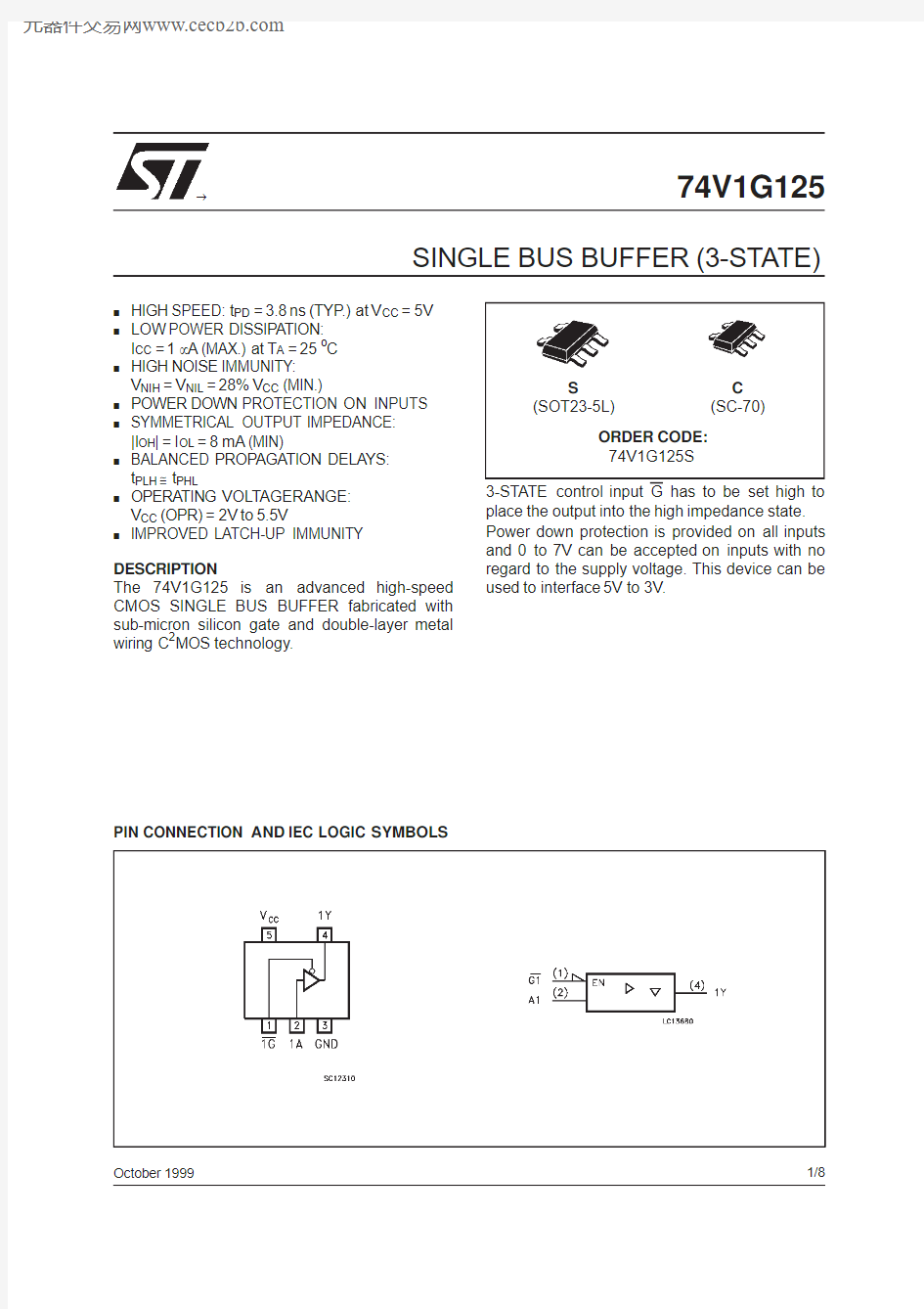
PIN CONNECTION AND IEC LOGIC SYMBOLS
?
S
(SOT23-5L)
C (SC-70)
ORDER CODE:74V1G125S
1/8
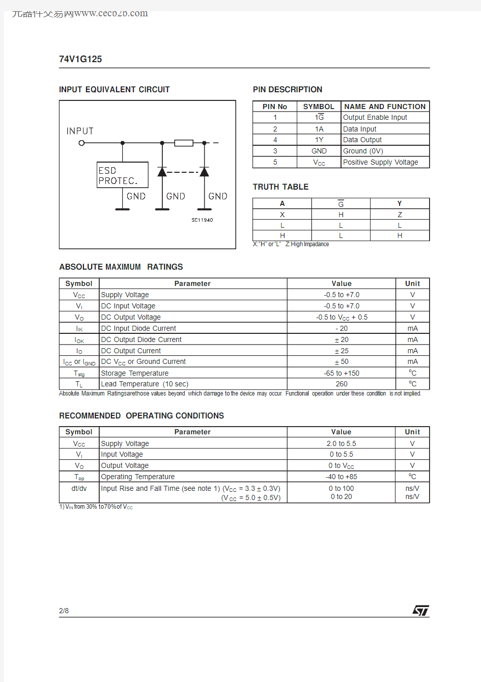
INPUT EQUIVALENT CIRCUIT
ABSOLUTE MAXIMUM RATINGS
Symbol Parameter
Value Unit V CC Supply Voltage -0.5to +7.0V V I DC Input Voltage -0.5to +7.0V V O DC Output Voltage -0.5to V CC +0.5
V I IK DC Input Diode Current -20mA I OK DC Output Diode Current ±20mA I O DC Output Current ±25mA I CC or I GND DC V CC or Ground Current
±50mA
T stg Storage Temperature -65to +150
o C T L
Lead Temperature (10sec)
260
o
C
Absolute Maximum Ratingsarethose values beyond which dam age to the device may occur.Functional operation un der these condition is not implied.
TRUTH TABLE
A G Y X H Z L L L H
L
H
X:”H”or ”L”Z:High Impadance
PIN DESCRIPTION
PIN No
SYMBOL
NAME AND FUNCTION 11G Output Enable Input 21A Data Input 41Y Data Output 3GND Ground (0V)
5
V CC
Positive Supply Voltage
RECOMMENDED OPERATING CONDITIONS
Symbol Parameter
Value Unit V CC Supply Voltage 2.0to 5.5V V I Input Voltage 0to 5.5V V O Output Voltage 0to V CC V
T op Operating Temperature
-40to +85o
C
dt/dv
Input Rise and Fall Time (see note 1)(V CC =3.3±0.3V)
(V CC =5.0±0.5V)
0to 1000to 20
ns/V ns/V
1)V IN from 30%to70%of V CC
74V1G125
2/8
DC SPECIFICATIONS
Symbol
Parameter
Test Conditions Value
Unit
V CC (V)
T A =25o
C -40to 85o
C Min.Typ.
Max.
Min.Max.
V IH High Level Input Voltage 2.0 1.5 1.5V 3.0to 5.50.7V CC
0.7V CC
V IL Low Level Input Voltage
2.00.50.5V
3.0to 5.50.3V CC
0.3V CC V OH
High Level Output Voltage
2.0I O =-50μA 1.9 2.0 1.9V
3.0I O =-50μA 2.9 3.0 2.9
4.5I O =-50μA 4.4 4.5
4.43.0I O =-4mA 2.58 2.484.5
I O =-8mA 3.94
3.8
V OL
Low Level Output Voltage
2.0I O =50μA 0.00.10.1V
3.0I O =50μA 0.00.10.1
4.5I O =50μA 0.0
0.10.13.0I O =4mA 0.360.444.5
I O =8mA 0.360.44I OZ
High Impedance Output Leakage Current
5.5V I =V IH or V IL V O =V CC or GND ±0.25
±2.5
μA
I I Input Leakage Current 0to 5.5V I =5.5V or GND ±0.1±1.0μA I CC
Quiescent Supply Current
5.5
V I =V CC or GND
1
10
μA
AC ELECTRICAL CHARACTERISTICS (Input t r =t f =3ns)
Symbol
Parameter
Test Condition Value
Unit
V CC (V)C L (pF)T A =25o
C
-40to 85o
C
Min.Typ.Max.
Min.Max.t PLH t PHL Propagation Delay Time
3.3(*)15 5.68.0
1.09.5ns
3.3(*)
508.111.5 1.013.05.0(**)15 3.8 5.5 1.0 6.55.0(**)50 5.37.5 1.08.5t PLZ t PHZ
Output Disable Time
3.3(*)15R L =1K ? 5.48.0 1.09.5ns
3.3(*)507.911.5 1.013.05.0(**)15 3.6 5.0 1.0 6.05.0(**)50 5.17.0 1.08.0t PZL t PZH
Output Enable Time
3.3(*)50R L =1K ?9.513.0 1.015.0ns
5.0(**)
50
6.1
8.5
1.0
10.0
(*)Voltag e range is 3.3V ±0.3V (**)Voltage range is 5V ±0.5V
74V1G125
3/8
74V1G125
CAPACITIVE CHARACTERISTICS
Symbol Parameter Test Conditions Value Unit
T A=25o C-40to85o C
Min.Typ.Max.Min.Max.
C IN Input Capacitance4pF
C OUT Output Capacitance61010pF
14pF
C P
D Power Dissipation
Capacitance(note1)
1)C PD isdefined as the value of the IC’sinternal equiva lent capacitance which is calculated fromthe operating current consumption without load.(Referto Test Circuit).Average operting curren t can be obtained bythe followingequa tion.I CC(opr)=C PD?V CC?f IN+I CC
TEST CIRCUIT
TEST SWITCH
t PLH,t PHL Open
t PZL,t PLZ V CC
t PZH,t PHZ GND
C L=15/50pF or equ ivalent(includes jigand probe capacitance)
R L=R1=1K?orequivalent
R T=Z OU T of pulse generator(typ ically50?)
4/8
74V1G125 WAVEFORM1:PROPAGATION DELAYS(f=1MHz;50%duty cycle)
WAVEFORM2:OUTPUT ENABLE AND DISABLE TIME(f=1MHz;50%duty cycle)
5/8
DIM.
mm
mils MIN.
TYP.
MAX.MIN.TYP.
MAX.A 0.90 1.4535.457.1A10.000.150.0 5.9A20.90 1.3035.451.2b 0.350.5013.719.7C 0.090.20 3.57.8D 2.80 3.00110.2118.1E 2.60 3.00102.3118.1E1 1.50 1.7559.068.8L 0.35
0.55
13.7
21.6
e 0.9537.4e1
1.974.8SOT23-5L MECHANICAL DATA
74V1G125
6/8
DIM.
mm
mils MIN.
TYP.
MAX.MIN.TYP.
MAX.A 0.80 1.1031.543.3A10.000.100.0 3.9A20.80 1.0031.539.4b 0.150.30 5.911.8C 0.100.18 3.97.1D 1.80 2.2070.986.6E 1.80 2.4070.994.5E1 1.15 1.3545.353.1L 0.10
0.30
3.9
11.8
e 0.6525.6e1
1.351.2SC-70MECHANICAL DATA
74V1G125
7/8
74V1G125
Information furnished is believed to be accurate and reliable.However,STMicroelectroni c s assumes no responsibility for the consequences of use of such information nor for any infringement of patents or other rights of third parties which may result from its use.No license is granted by implication or otherwise under any patent or patent rights of STMicroelectroni c s.Specification mentioned in this publication are subject to change without notice.This publication supersedes and replaces all informati o n previously supplied.STMicroelectronics products are not authorized for use as critical components in life support devices or systems withoutexpress written approval of STMicroelectronics.
The ST logo is a registered trademark of STMicroelectronics
?1999STMicroelectronics–Printed in Italy–All Rights Reserved
STMicroelectronics GROUP OF COMPANIES
Australia-Brazil-China-Finland-France-Germany-Hong Kong-India-Italy-Japan-Malaysia-Malta-Morocco
Singapore-Spain-Sweden-Switzerland-United Kingdom-U.S.A.
https://www.360docs.net/doc/f03976104.html,
.
8/8