BSP452中文资料
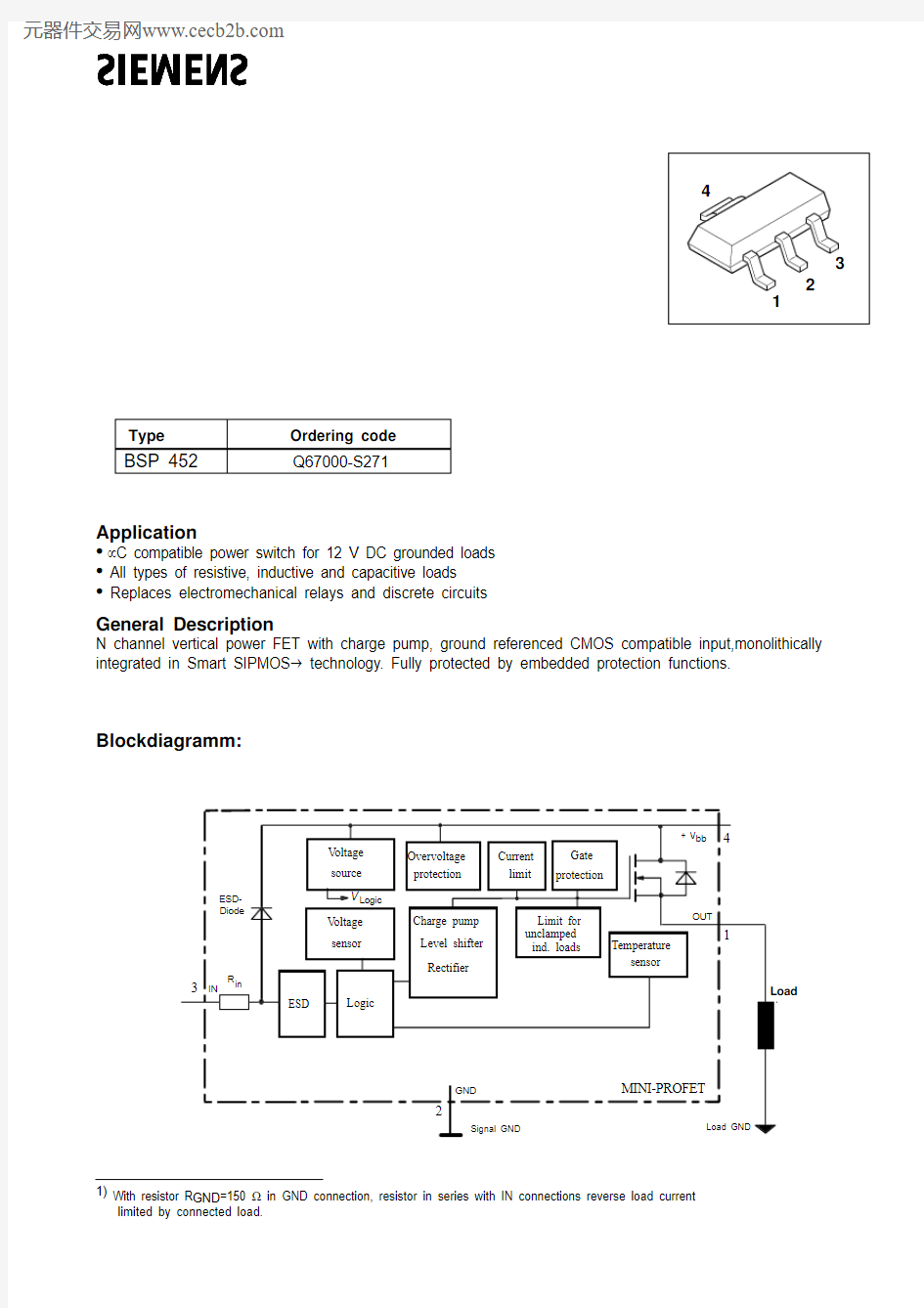
Application
?μC compatible power switch for 12 V DC grounded loads
? All types of resistive, inductive and capacitive loads
? Replaces electromechanical relays and discrete circuits
General Description
N channel vertical power FET with charge pump, ground referenced CMOS compatible input,monolithically integrated in Smart SIPMOS? technology. Fully protected by embedded protection functions.
Blockdiagramm:
GND=150 ? in GND connection, resistor in series with IN connections reverse load current
limited by connected load.
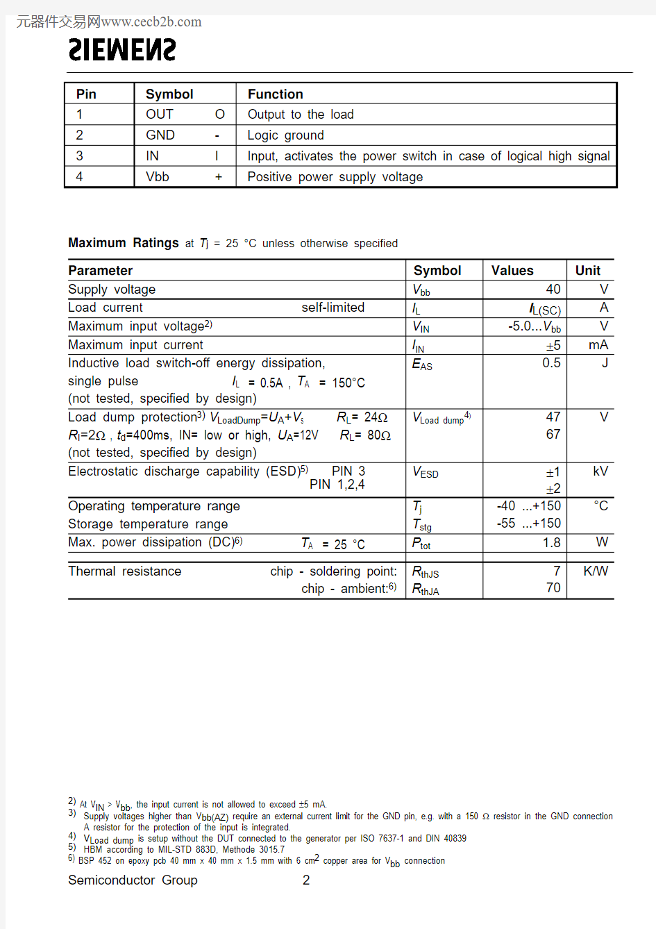
Maximum Ratings at T j = 25 °C unless otherwise specified
2) At V
IN > V bb, the input current is not allowed to exceed ±5 mA.
3)Supply voltages higher than V
bb(AZ) require an external current limit for the GND pin, e.g. with a 150 ? resistor in the GND connection
A resistor for the protection of the input is integrated.
4)V
Load dump is setup without the DUT connected to the generator per ISO 7637-1 and DIN 40839
5)HBM according to MIL-STD 883D, Methode 3015.7
6) BSP 452 on epoxy pcb 40 mm x 40 mm x 1.5 mm with 6 cm2 copper area for V
bb connection
Input turn-on threshold voltage
IN(T-)
7) I
L(ISO) characterizes the MOSFET part of the device and may be higher than the shortcircuit current I L(SC) of the whole device
8)At supply voltage increase up to V bb = 5.6 V typ without charge pump, V
OUT ≈V bb - 2 V
9)While demagnetizing load inductance, dissipated energy in PROFET is E AS = ∫ V
ON(CL) * i L (t) dt, approx.
E AS = 1/2 * L * I 2L * (
V ON(CL)V ON(CL) - V bb
)10)Requires 150 ? resistor in GND connection. Reverse load current (through intrinsic drain-source diode) is normally limited by the
connected load.
Max. allowable power dissipation P tot = f (T A ,T SP )P tot
[W]
02468
10
12
1416180
25
50
75
100
125
150
T A, T SP [°C]On state resistance (Vbb-pin to OUT-pin)R ON = f (Tj); V bb = 13.5 V; I L = 0.5 A
j Current limit characteristic
I L(SC) = f (V on ); (V on see testcircuit)I L(SC) [A]
00.20.40.60.8
1
1.21.41.61.820
2
4
6
8
10
12
14
V on [V]
Typ. input current
I IN = f (V IN ); V bb = 13,5 V I IN [μA]
0510
1520253035
404550
2
4
6
8
10
12
14
V IN [V]
Typ. operating current
I GND = f (T j ); V bb = 13,5 V; V IN = high I GND
[mA]
00.10.20.30.4
0.5
0.60.70.8-50
-250255075100125150T j [°C]
Typ. standby current
I bb(off) = f (T j ); V bb = 13,5 V; V IN = low I bb(off)
[μA]
01234
5
678-50
-25
25
50
75
100
125150
T j [°C]Typ. overload current
I L(lim) = f (t); V bb = 13,5 V, no heatsink, Param.: T jstart I L(lim) [A]
0.2
0.4
0.6
0.8
1
1.2
1.4
-50050100150200250300350400
t [ms]
Short circuit current
I L(SC) = f (T j ); V bb = 13,5 V
I L(SC) [A]
00.20.40.6
0.8
11.21.4-50
-250255075100125150
T j [°C]
Typ. input turn on voltage threshold V IN(T+) = f (T j );V IN(T+) [V]
00.5
1
1.5
2
2.5
3
-50
-25
25
50
75
100
125
150
13V
T j [°C]Typ. on-state resistance (Vbb-Pin to Out-Pin)R ON = f (V bb ,I L); I L =0.5A, T j = 25°C R ON [m ?]
050
100
150
200
250
300
5
10
15
20
25
V bb [V]
Figure 6: Undervoltage restart of charge pumpe
V ON [V]
V bb [V]
charge pump starts at V bb(ucp) about 7 V typ.
Test circuit