纳米p型SiC-硅橡胶复合材料高压非线性I-V机理研究
1070-9878/10/$25.00 ? 2010 IEEE
Mechanisms Leading to Nonlinear Electrical Response
of a Nano p -SiC/Silicone Rubber Composite
X. Wang, J. K. Nelson, L. S. Schadler
Rensselaer Polytechnic Institute
110 Eighth Street Troy, NY 12180, USA and H. Hillborg,ABB Corporate Research
V?ster?s, Sweden
ABSTRACT
It is we ll known that hopping of charge carrie rs via spatially and e ne rge tically distribute d localize d state s is a primary transport me chanism in many disorde re d se miconductors and polyme ric die le ctrics. In this contribution, the nonline ar I-V physics of a 25vol% 50nm p -SiC/silicone rubbe r composite for high voltage fie ld grading application was inve stigate d, and a composite bulk hopping me chanism propose d. It is hypothe size d that ne are st-ne ighbor hole hopping occurs through thin rubbe ry laye rs be twe e n the SiC particle s, and is the me chanism gove rning the nonlinear electric response of SiC/silicone rubber nanocomposites.
Index Terms —Nonlinear electrical, mechanism, high field, hole hopping transport, nearest-neighbor, thin rubbery layer, field grading, nanocomposite.
1 INTRODUCTION
HIGH-VOLTAG E E-field grading [1-4] is typically
implemented via the use of composites with high dielectric constant or composites that possess desirable high field nonlinear resistive behavior. The latter, high field nonlinear resistive field grading composites [4-10], which serve to avoid excess electrical stress concentrations under both ac and dc applications, are commonly made of an insulating polymer matrix, especially rubber such as ethylene propylene diene monomer (EPDM) or silicone rubber, loaded with conducting carbon black, and/or ceramic semiconductor such as SiC, ZnO, or even an organic semiconductor like polyaniline emeraldine base.
In general, the I-V dependence of nonlinear field grading composites can be described by a simple empirical power-law equation D V I v (?>1).The real physics behind this empirical electrical response, however, has not been rigorously studied. It is commonly speculated that, at loadings below percolation, two competing mechanisms such as tunneling [11-13] or hopping [13-19] across thin polymer matrix layers separating filler particles dictate the composite I-V nonlinearity. Above
percolation when direct filler pathways are formed, the
composite nonlinear behavior may be the result of carrier tunneling or field-assisted thermionic emission across particle contact double Schottky barriers similar to the behavior
governing varistors [20-22]. On the other hand, mechanisms like electrode Schottky injection [23-25], bulk Poole-Frenkel emission [26-29] as well as space charge-limited currents [30-31] could also dominate or contribute to the overall composite I-V nonlinearity.
Among the proposed mechanisms, hopping of charge carriers across spatially, as well as energetically discrete, localized states has been widely reported to be a primary charge transport mechanism in many amorphous semiconductors, dielectrics or composites [32-38]. In such cases, carrier hopping usually takes place between neighboring sites of small separation, called nearest-neighbor hopping,or between sites of close energy level but slightly larger separation, called variable range hopping, which is more favorable at low temperature. In this paper, a detailed set of electrical characterization and data analysis leads to a hypothesis of valence band tail nearest-neighbor hole hopping as the mechanism governing the high field I-V nonlinear behavior in nano p -SiC/silicone rubber composites.
2 EXPERIMENTAL The SiC powder filler used in this study was 50 nm in diameter and of beta phase. Secondary-ion mass
spectroscopy (SIMS) characterization done by the Evans
analytical company determined the SiC powder doping level
Manuscript received on 22 April 2010.
and type. A pure 800-1,200 cSt low viscosity polydimethylsiloxane (trimethylsiloxy terminated, vinylmethylsiloxane (0.8-1.2 mole%)-dimethylsiloxane (99.2-98.8 mole%) copolymer) from Gelest Inc. was used as
the matrix silicone resin.
The 25vol% 50nm-SiC/silicone rubber which displayed the highest composite I-V nonlinearity in a preliminary study, was selected to study the nonlinear I-V mechanism. The composites were prepared by mixing nano-SiC powder with silicone resin at the appropriate ratio in a Hauschild ?high speed mixer. 1wt.% dicumyl peroxide was employed as the silicone rubber crosslinking agent. Samples were compression moulded at 150 q C/1h +180 q C/1h. Prior to any electrical tests, the cured composite discs (approximately 0.5 mm in thickness) were kept in a vacuum oven at ~80 °C
overnight to remove any dicumyl peroxide residue, and gold electrodes of 2 cm in diameter were then sputter deposited
onto both surfaces of the discs. Robust composite as well as SiC powder filler high field I-V characterization was performed either in a customized guarded cell for composites or a powder measurement cell for powders,
which was connected to a Keithley 6517A electrometer and biased with a Bertan 10 kV voltage source. The measurements were generally undertaken at a range of temperatures at or above ambient temperature. To help identify the underlying conduction mechanism, additional composite I-V
measurements were done at a dry ice temperature (~-40 °C).
Steady-state composite or powder current readings were
typically taken 2 h (composites) or 1 min (powders) after the
step voltage was turned on. Some composite transient currents were also recorded with a L abview 6i program for an
absorption current study.
In addition, dielectric spectroscopy measurements were
undertaken using a Novocontrol Alpha Analyzer. The test ac
voltage was 1 volt RMS, and the typical measurement
conditions were: 1 mHz to 0.1 MHz, 30 °C to 120 °C. Pulsed
electro-acoustic (PEA) measurements [39-40] were conducted to assess the internal space charge distribution in the composite at room temperature. The applied dc field for space charge measurement ranged from 7 to 12 kV/mm. The interrogating pulse amplitude was 500 V, with a pulse width of about 10 ns. 3 RESULTS
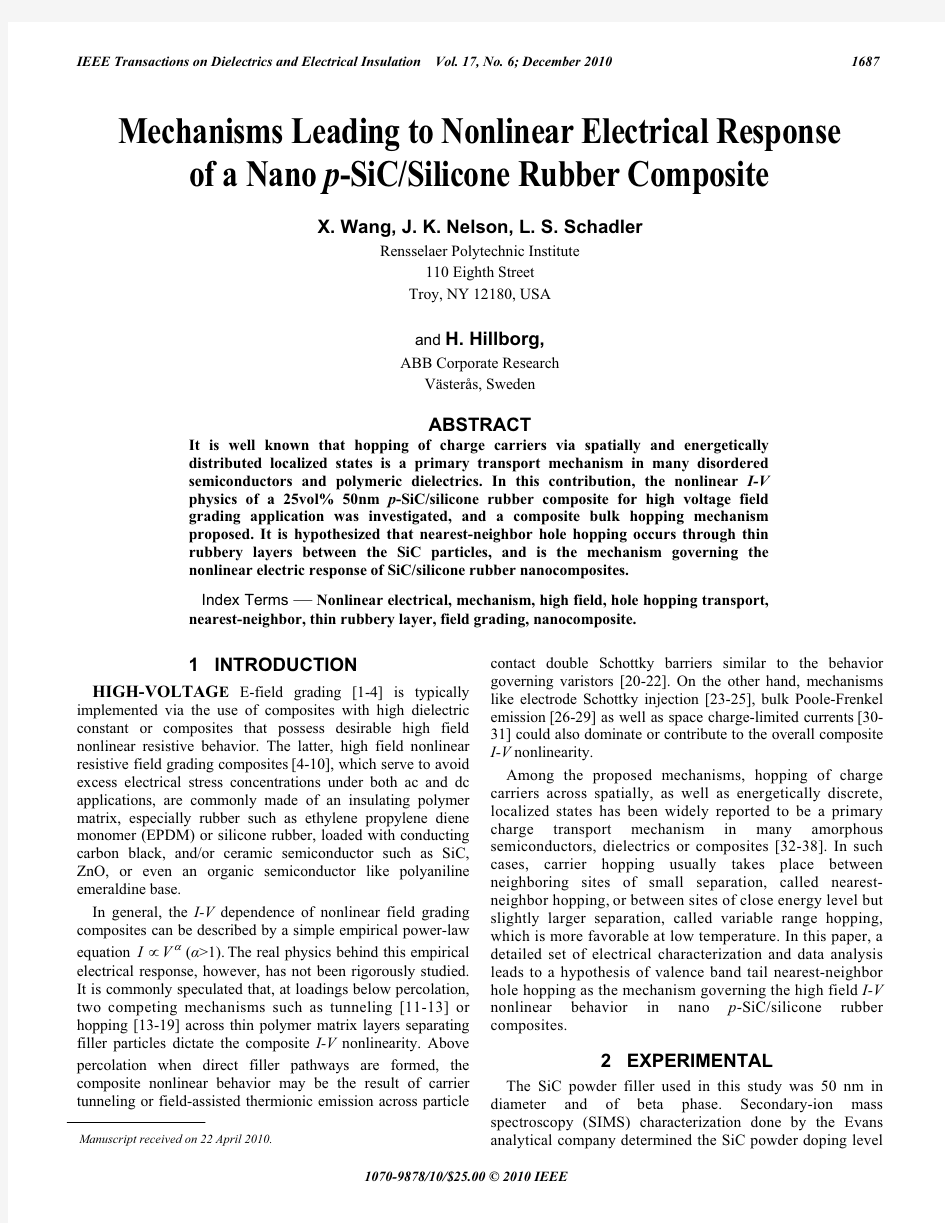
3.1 SIC POWDER AND BASE SILICONE RUBBER The composite filler, a nano SiC powder, was characterized by secondary-ion mass spectroscopy and found to be p -type with an Al impurity of ~0.9×10²⁰ atoms/cm 3. Electrical characterization revealed that the nonlinear I-V behavior or current density (J ) as a function of electric field (E ) for the SiC powder compact was slightly temperature dependent, as shown in Figure 1.The powder nonlinearity exponent, D , was found to be approximately 4 at ambient temperature, which is better illustrated in the inset plot of powder resistivity vs. field. From an Arrhenius plot (ln J vs. 1000/T) at constant fields, the average charge carrier activation energy ?E for the nano-SiC
Figure 2 shows the dielectric spectroscopy data for the base
silicone rubber, i.e., neat crosslinked silicone resin. A similar
silicone rubber dielectric spectroscopy result was reported by others [41].The data in the range 0.1-10 Hz is of particular interest. The slope of the log(?”) (the imaginary permittivity) vs. log(frequency) is approximately 1, whereas the real permittivity, ?’, remains almost constant. This is typically a sign of dc conduction [42-44]. It suggests that the silicone rubber is a strongly disordered hopping carrier system in which the charge carriers can hop between localized sites, thereby introducing some dc conduction. 3.2 COMPOSITE DISPERSION & NONLINEAR BEHAVIOR A typical Field Emission Scanning Electron Microscopy dispersion image of the 25vol% 50 nm-SiC/silicone rubber (SIR) composite is shown in Figure 3. The composite dispersion seems uniform although there are signs of some particle agglomeration, and it also appears that most particles are not in direct contact with each other. The composite steady -state nonlinear current density vs.
field and the log(resistivity) vs. log(field) measured at a series of temperatures are shown in Figure 4(a-b). The data indicate that the composite starts to display nonlinearity at fields
beyond 2-4 kV/mm, and the nonlinearity exponent, ?,generally drops as temperature increases. Furthermore, compared to the nano-SiC powder compact, the nonlinear J -E behavior of the composite has larger temperature dependence. Corresponding Arrehnius plots (ln J vs. 1000/T) indicate that the composite carrier activation energy is ~0.4-0.6 eV, which is almost one order of magnitude higher than that of the powder compact. This implies that there are likely no significant direct particle-particle contact pathways in the composite, i.e., the 25vol% nanocomposite is below its geometric percolation and most SiC particles are separated by a thin silicone rubber layer.
Figure 1.The nano-SiC powder current density J vs. electric field E at
different temperatures. The inset plot shows powder resistivities at 25q C.
Theoretically, the average inter-particle silicone rubber layer thickness can be estimated based on the following equation for spherical fillers under ideal uniform dispersion [45-46]:
?
???
o
????
a ??1·¨¨?§ 2343
1f r l S (1) where l is the inter-particle distance, r the particle radius, and f the filler volume fraction. Accordingly, the average inter- particle silicone rubber layer thickness for the 25vol% 50 nm-SiC/silicone rubber is calculated to be approximately 14 nm.
3.3 COMPOSITE HOLE HOPPING NONLINEAR
HYPOTHESIS
3.3.1 HOLE HOPPING HYPOTHESIS
Hole injection and transport is acknowledged as a primary charge carrier process in many amorphous polymeric dielectrics [47-51]. Hole hopping conduction has also been identified as a primary conduction mechanism in some systems, e.g., in the amorphous regions of insulating polyethylene [47]. In this study, a high field nonohmic hole hopping transport at silicone rubber valence band tail hypothesis is schematically shown in Figure 5. The energy levels are based on the electronic band configuration of the components. In this figure, the electrodes are sputtered gold coatings, with a Work Function of ~5 eV. The bottom of the conduction band for silicone rubber is assumed to be located near the vacuum level, which is typical for most organic dielectrics [47, 50-51]. The band gap of ?-SiC is around 2.2 eV [52-54], and the bottom of the conduction band is taken as 2.9eV below the vacuum level [52].
Hole injection and transport is hypothesized to be the dominant carrier process in the schematic based on the following two arguments. First, electrode hole injection is more likely to occur because the Schottky barrier height should be much lower compared to that for electron injection. For instance, if we assume the silicone rubber band gap is 6~8
Figure 2.Real, and imaginary permittivity vs. frequency for base silicone rubber. The data within 0.1-10 Hz is a likely indication of hopping conduction.
1.0
10.0
100.0
1.0E-3
1.0E-1
1.0E+1 1.0E+3
1.0E+5
f, Hz
?'
1.0E-4
1.0E-2
1.0E+0
1.0E+2
1.0E-3
1.0E-1
1.0E+1 1.0E+3
1.0E+5
f, Hz
?''
Figure 3. A Field Emission SEM image of the 25vol% 50nm-SiC/silicone rubber composite showing the state of dispersion.
Figure 4.25vol% 50nm-SiC/silicone rubber composite (a) steady-state current density vs. field at various temperatures, and (b) corresponding log(resistivity) vs. log(field) plots.
h +
hop
hop
hop
e -
2.2 eV
CB bottom 2.9eV 2.2 eV
CB bottom 2.9eV
Figure 5.The speculated hole injection and conduction occurred for the 25vol% 50nm p -SiC/SIR composite. The (nearest-neighbor) hole hopping across thin silicone rubber layer VB tail process is hypothesized to be the governing physics for composite high field I-V nonlinearity. The overall band tilting under the field is removed for clarity.
eV, then the hole injection barrier height is around 1-3 eV, whereas the barrier height for electron injection is about 5 eV. Second, even if there are injected electrons, they will likely recombine with holes in p -SiC, therefore not contributing much to the steady-state current. The overall charge process may occur as follows: holes (h +) are Schottky injected from the anode, which travel through the neighboring thin rubbery layer via hopping across localize states near the silicone rubber valence band (VB) tail, followed by bulk conduction in the SiC VB. After that, it is postulated that holes are further internally emitted from p -SiC VB to the VB of the neighboring silicone rubber layer, followed by hopping transfer through that silicone rubber layer and so on, until eventually recombining with electrons at the cathode.
3.3.2 NEAREST-NEIGHBOR HOPPING (NNH) MECHANISM
Because variable range hopping can be ruled out based on the discussion in section 3.4.3 later on, nearest-neighbor
hopping is the primary mechanism addressed here.
A. NNH EQUATION MODIFICATION For classical thermally-activated, field-enhanced “nearest-neighbor” middle band gap or impurity band hopping near the Fermi level,the conductivity is derived as follows [14-19]:
a) It is assumed that the number of electrons per unit volume
within a range kT of the Fermi energy is kTN(E F ), where k is Boltzmann’s constant, and N(E F ), the density of local states at the Fermi level.
b) The hopping rate is approximately given by the phonon-induced hopping probability difference towards and against the electric field, which approximately equals:
)]/exp()/[exp()/exp(kT eRE kT eRE kT E hop ph ' Q (2)
where ?Ph is phonon frequency, ?, the reciprocal of the decay length of the localized wave function, and R ,?E hop are the average hopping distance and the average hopping activation energy respectively. c)Current density J is obtained by multiplying the above two terms with e and R, which gives:
)
/sinh()/exp()(kT eRE kT E E eRkTN J hop Ph F ' Q
(3) In this work, we hypothesized a carrier transport process governed by nearest-neighbor hole hopping across the silicone rubber VB tail. As a result, the above carrier population term
)(F E kTN for middle band gap impurity hopping conduction should be replaced with the hole density near the SiC/silicone rubber interfaces, which conceptually is roughly proportional to exp(-E A /2k T), where E A is the SiC acceptor level, reported to be ~0.25 eV [52]. If we further assume h kT Ph / Q , then equation (3) becomes
)/sinh()/2(exp(kT eRE kT E E h kT eR J A hop ' v (4)
or ))(sinh()(E T D T C J , where C(T) and D(T) are as follows:
)/)2
(exp()(kT E E h kT
eR T C A hop ' v (5a) and kT eR T D /)( (5b) In addition, to achieve a more appropriate comparison of equation (4) with the data, a local E -field instead of nominal E -field is needed. This field can be determined simply by
assuming that the dc voltage drop occurs only at the insulating rubber layers. The local E -field at each silicone rubber layer then approximately follows:
)/1(/)(00l d E l d l E E local | (6) where E 0 is the nominal electric field, l the inter-particle
silicone rubber layer thickness, d the SiC particle diameter (~50 nm). Recall that from equation (1), the average silicone rubber layer thickness l for the studied nanocomposite is about 14 nm. Accordingly, E local is derived to be about 4-5 times higher than the nominal field.
B. NEAREST-NEIGHBOR HOPPING FITTINGS Results suggest that the experimental data fit well with the two parameter hyperbolic sine function characterized for nearest-neighbor hopping at each temperature, as shown in Figure 6(a-e). A further plot of ln(C(T)/T ) vs. 1/T shown in Figure 7(a) exhibits a clear linear trend, from the slope of which, the overall hopping activation energy, ?E hop +E A /2, is estimated to be about 0.53 eV according to equation (5a), which falls in the 0.4-0.6 eV range derived from the composite Arrhenius ln J -1/T fitting. The net hopping activation energy, ?E hop , is accordingly given as 0.53 eV - 0.25/2 eV § 0.41 eV. Figure 7(b) shows the D(T) vs. 1/T fitting, which can be roughly fitted to follow a linear trend that intersects the origin (0,0). The overall average hopping distance, R , is then estimated to be approximately 4.3 nm according to equation (5b). From the same equation, the individual hopping distance, R , at each temperature can also be obtained from each D parameter, as listed in Table 1.
Table 1.Derived individual hopping distance R at each temperature.Temperature, °C 25 60
80
100
120
Hopping distance, nm
~4.8
~3.6 ~4.0 ~3.5 ~4.0
Figure 6.25vol% nano-SiC/SIR composite J-E local two parameter hyperbolic sine hopping fittings (a)-(e).
Fitting parameter C and D at each temperature are shown on each figure.
Figure 7.25vol% nano-SiC/SIR (a) ln(C/T ) vs. 1/T , and (b) D(T) vs. 1/T hopping fittings.
0.0E+00
5.0E ?08
1.0E ?071.5E ?07
2.0E ?072.5E ?07
0.001
0.0020.0030.004
1/T, K
?1
D (T )
-30
-26
-22-18
0.0024
0.0029
0.0034
0.0039
1/T, K
-1
l n C (T )/T
Figure 8.A plot of kT ·ln(J/T 2) vs. E 1/2 to compare the data to the Schottky model for a 25vol% 50nm-SiC/SIR composite.
-0.9
-0.7
-0.5
1.0E+3
1.5E+3
2.0E+3 2.5E+3
3.0E+3
sqrt(E)
K T l n (J /T 2
)
3.4 ALTERNATIVE MECHANISMS
3.4.1 ELECTRODE INJECTION
Electrode charge injection can prevail over bulk conduction mechanism in real measurements. It commonly takes place by field-assisted thermionic emission, i.e., Schottky emission or by simple tunneling injection. Tunneling injection can basically be ruled out in this case because the nano-SiC/SIR J-E data show significant temperature dependence. For electrode
Schottky injection, the J-E relationship obeys the following
equation [23-25]:
equals 1202 mA/mm 2K 2). ?Sch is the Schottky constant, ?0 and ? are the vacuum permittivity and high frequency dielectric constant of the material (SIR in this case).
Figure 8 shows the )/ln(2T J kT ~E 1/2plots for the nano-SiC/SIR at all measured temperatures, which seem to follow
straight lines. From the slope ?Sch ,? for silicone rubber matrix
is calculated to be about 0.22, which is one order of magnitude
lower than what was measured in Figure 2(a) as well as the
commonly reported ? of ~3 [41]. This discrepancy in
dielectric constant rules out electrode Schottky injection as the underlying mechanism leading to composite nonlinearity, and implies that the external carrier supply is abundant.
3.4.2 INTERNAL TUNNELING OVER THIN SIR LAYER Tunneling through a thin polymer layer is an important charge transport mechanism. The general conditions for tunneling to occur are: 1) the local E-field should be high enough, for instance, 100 kV/mm; and 2) the polymer layer should be thin enough, typically within 2~3 nm. In the studied 25vol% 50nm-SiC/SIR system, the composite nonlinear behavior starts at fields as low as ~2 kV/mm, which is far below the 100 kV/mm even after taking into account the estimated 4 ~ 5 × local field enhancement. In the meantime, the average silicone rubber layer thickness is calculated to be ~14 nm. Both of these argue against direct internal tunneling.
Furthermore, since the p -SiC hole density is proportional to exp (-E A /2kT ), the temperature dependence (if tunneling only
were occurring) would have a maximum activation energy of
E A
/2, i.e., ~0.13 eV, which is still considerably lower than the
activation energy range of 0.4-0.6 eV estimated from the composite Arrehnius fittings. 3.4.3. VARIABLE RANGE HOPPING OVER A THIN
SIR LAYER
Hopping through a thin polymer layer usually takes place through either variable range hopping (VRH) or nearest-neighbor hopping (NNH). The temperature dependence of the conductivity for both hopping mechanisms follows [32-33, 36]: ))/exp((00s T T V V (8) For variable range hopping, s is typically ?, which gives the well known three-dimensional Mott’s law, whereas nearest-neighbor hopping is identified by a single thermal activation
process, where s is equal to 1. A typical composite ln(conductivity) as a function of 1/T plot is shown in Figure 9, which includes a data point on dry
ice temperature. The data suggest that a transition in
mechanism occurs below room temperature. Above room
temperature, a single thermal activation process, i.e., nearest-neighbor hopping occurs, whereas variable range hopping may
take place at low temperature.
For quantitative analysis, the composite ln(conductivity) vs. 1/T 0.25was plotted and is shown in the inset plot of Figure 9. According to the literature [36-37], in the event of Mott variable range hopping, the fitting parameters ?0and T 0 are closely related to the density of local states at the Fermi level, N(E F ), and the decay length of the localized wave function, ?-1
, within the material as given in equations (9a-9b):
)
(1.183
0F B E N k T
D (9a)
Nano-SiC/SIR. The inset plot shows the corresponding composite ln(conductivity) vs. 1/T 0.25Mott’s variable range hopping fitting at ambient temperature & above.
ph B F e T k E N Q SD V 2
2
/108)(9 ?
o
??a (9b)
Further knowledge such as the average hopping distance, R , or the hopping activation energy, ?E hop can be obtained from equations (9c-9d).
4
/1)(89
??
1ᬬ?
§ F B E TN k R SD (9c)
)
(43
3F hop E N R E S
' (9d)
The result indicates that T 0 and ?0 are around K 9
1067.2u and 1101006.1 u m S respectively. Reasonable calculated values of N(E F ), R and ?E hop are ~1317103.6 u eV cm ,~10.2nm and ~0.35eV at ambient temperature after taking 51 D ?. The phonon frequency ?ph derived from equation (9b) is ~120107.9 u s , which is however significantly higher
than practical phonon frequency of ~1
12106 u s near room temperature. This helps rule out variable range hopping as the primary charge conduction mechanism. 3.4.4 SPACE-CHARGE OR POOLE-FRENKEL EFFECT
A classical space-charge-limited current model [30-31] like the Mott-Gurney law generally predicts a constant low nonlinearity exponent, ?, of close to 2, according to: 2
08
9L
V J PHH (10) which cannot explain the J-E nonlinearity for the studied
nano-SiC/SIR. On the other hand, compared to the hopping mechanism, the Poole-Frenkel effect [26-29] is typically associated with low density yet deep level localized sites or traps (~>1 eV) in dielectrics, which is higher than the estimated composite activation energy of 0.4-0.6 eV. In addition, the dielectric spectroscopy data suggested that the base silicone rubber is likely a hopping carrier system with a high density of local states. Therefore, the Poole-Frenkel mechanism can also be ruled out.
3.5 OTHER RESULTS
3.5.1 COMPOSITE ABSORPTION CURRENT
CHARACTERIZATION
Absorption current characterization [55-57] often provides additional insight for understanding the carrier injection and charge transport in a non-ideal dielectric. Figure 10 shows the nanocomposite room temperature absorption current as a function of time at different fields: from the low field, composite linear I-V region of 2 - 4 kV/mm, to fields of 6 - 8 kV/mm in the nonlinear region (refer to Figure 4b). The result indicates that, in a log-log representation, the low field absorption current follows a linear universal law [55-57], i.e.
n
t T A t I )()(, with n close to unity. By contrast, the current drop slows down and a plateau gradually forms at high
(nonlinear) fields, rendering appreciably higher steady-state currents at high fields. According to Jonscher [57], this high field plateau can be attributed to a carrier hopping mechanism, which supports our hopping hypothesis.
3.5.2 COMPOSITE DIELECTRIC SPECTROSCOPY
Figure 11 shows the nano-SiC/SIR dielectric loss, ?”, as a function of frequency at different temperatures. At low frequency, ?”displays a rapid increase, and the data at each
temperature are essentially parallel, which is likely an
indication of thermally-activated quasi-dc conduction. Based
on the loss frequency shift as a function of 1/T (the insert plot), the activation energy, ?E , is found to be about 0.54 eV, which indeed agrees well with the overall 0.53 eV activation
energy derived from the nearest-neighbor hopping fitting in section 3.3.2.
3.5.3 PULSED-ELECTROACOUSTIC (PEA) STUDY
Pulsed-electroacoustic analysis (PEA) [39-40] was undertaken on the 25vol% nano-SiC/SIR composite. The charge buildup at typical field of 7 kV/mm is shown in Figure 12. The data show no sign of homocharge near the cathode for electrode injection, whereas there exists a uniform positive charge buildup across the composite, which could be argued as
a sign for hole conduction.
from low, linear to high, nonlinear fields.
shows log f vs. 1000/T .
4 DISCUSSION The logic for the composite nonlinearity drop as temperature increases can be understood on the basis of nearest-neighbor hopping conduction as follows. First, in terms of fundamental physics, the composite hopping nonlinearity exponent, ?, basically arises from the hopping
probability difference along or against the field, which is expected to be compromised as T increases. Second, mathematically, the hopping nonlinearity, ?, is determined by
the field dependent term )/sinh(kT eRE , which is approximately equal to 2/)/(kT eRE e at high fields. Accordingly,
D E e kT eRE
J kT eRE v v 2/)sinh()/( (11) .ln ~const E
E kT eR D (12)
Equation (12) suggests that the hopping nonlinearity exponent,
?, should decrease as T increases, and it also implies that, ?, is indeed field dependent. Furthermore, the hypothesis of hole hopping across the
silicone rubber valence band tail is largely based on an ideal component band configuration as well as the p -type nature of the filler SiC. When the composite system is
different, hopping could also occur in the middle of the band gap near the Fermi level, or through the organic conduction band tail for electron hopping if the fillers are
n -type semiconductors, metals or carbon black. Finally, an ionic hopping contribution, which has been claimed for some organic dielectric or dielectric composites, cannot be
rigorous ruled out in this study [35, 38], as it also happens
via hopping transfer. 5 CONCLUSIONS A robust investigation has been performed to study the high field nonlinear I-V mechanism for a 25vol% 50nm p -SiC/silicone rubber field grading composite. Results indicate
that thermally-activated, field-enhanced nonohmic hole nearest-neighbor hopping transport across inter-particle silicone rubber layers is likely the mechanism governing the nonlinear behavior. The average hopping activation energy
and average hopping distance are estimated to be ~0.41 eV and ~4.3 nm respectively, both of which are typical for hopping conduction, and the hopping-based composite nonlinearity exponent, ?, generally decreases as temperature increases.
ACKNOWLEDGEMENT
The authors are grateful for the sponsorship from ABB Corporate Research, Sweden, through the Rensselaer
Nanotechnology Center, and the Nanoscale Science and Engineering Initiative of the National Science Foundation under NSF award number DMR-0642573. We would also
like to express sincere gratitude to Dr. Uno G?fvert and Dr.
Mikael Unge at ABB Corporate Research for very helpful discussions. REFERENCES [1] A. Roberts, “Stress Grading for High Voltage Motor and
Generator Coils”, IEEE Electr. Insul. Mag., Vol. 11, No. 4, pp. 26-31, 1995.
[2]S.V. Nikolajevic, N.M. Pekaric-Nad and R.M. Dimitrijevic, “Optimization of Cable Terminations ”, IEEE Trans. Power
Delivery, Vol. 12, pp. 527-532, 1997.
[3]
R. Strobl, W. Haverkamp, G. Malin and F. Fitzgerald, “Evolution
of Stress Control Systems in Medium Voltage Cable Accessories”, Transmission and Distribution Conf. Exposition, IEEE/PES, Vol. 2, pp. 843-848, 2001. [4]G. L upò, V. Tucci, N. Femia and M. Vitelli, “Electrical Field Calculation in HV Cable Terminations Employing Heat-Shrinkable Composites with Non Linear Characteristics”, IEEE 4th
Intern. Conf. Properties and Applications of Dielectric Materials,
Australia, pp. 278-281, 1994. [5]L . Egiziano, V. Tucci,G. L upò and C. Petrarca , “Electrical Properties of Different Composite Materials for Stress Relief in HV Cable Accessories ”, IEEE Conf. Electr. Insul. Dielectr. Phenomena (CEIDP), pp. 110-113, 1995.
[6] E. M?rtensson, B. Nettelblad, U. G?fvert and L . Palmqvist, “Electrical Properties of Field Grading Materials with Silicon
Carbide and Carbon Black”, IEEE Intern. Conf. Conduction and Breakdown in Solid Dielectrics, Sweden, pp.548-552, 1998.
[7] C. ?nneby, E. M?rtensson, U. G?fvert, A. Gustafsson and L . Palmqvist, “Electrical Properties of Field Grading Materials
Influenced by the Silicon Carbide Grain Size”, IEEE 7th Intern. Conf. Solid Dielectrics, Netherlands, pp. 43-45, 2001.
[8]T. Oksmoto, I. Yoshiyuki, M. Kawahara, T. Yamada and S. Nakamura, “Development of Potential Grading L ayer for High
Voltage Rotating Machine”,IEEE Intern. Symposium on Electrical Insulation, Indianapolis, USA, pp. 210-215, 2004.
[9]J. Pelto, M. Paajanen, K. Kannus, K. L
ahti and P. Harju,
“Nonlinear DC Voltage-Current Characteristics of New Polymeric
Composite Materials Based on Semiconductive Polyaniline Emeraldine Base Filler”,IEEE Intern. Conf. Solid Dielectrics, Toulouse, France, 2004.
[10]. Donzel, T. Christen, R. Kessler, F. Greuter and H.
Gramespacher, “Silicone Composites for HV Applications Based on Microvaristors”, IEEE Intern. Conf. Solid Dielectrics, France,
2004.
[11]I. Balberg, D. Azulay, D. Toker and O. Millo, “Percolation and
Tunneling in Composite Materials”, Intern. J. Modern Physics B,
Vol. 18, pp. 2091-2121, 2004. [12]I. Balberg, “A Comprehensive Picture of the Electrical Phenomena in Carbon Black-Polymer Composites”, Carbon, Vol. 40, pp. 139-143, 2002.
SiC/SIR for charge buildup at 7 kV/mm.
[13] A Celzard, E. McRae and G. Furdin, “Conduction Mechanisms in
Some Graphite-Polymer Composites: the Effect of a Direct-Current Electric Field”, J. Phys.: Condens. Matter. Vol. 9, pp. 2225-2237, 1997.
[14]N. M. Mott, Electronic Processes in Non-crystalline Materials,
chapter 2, 1979.
[15]H. B?ttger, Hopping Conduction in Solids, VHC, Berlin, 1985.
[16]M. Pollak and B. Shklovskii, Hopping Transport in Solids, North-
Holland, 1991.
[17]H. Fritzsche and M. Pollak, “Hopping and Related Phenomena”,
Advances in Disordered Semiconductors, Vol. 2, pp. 299-308, 1990. [18]R. M. Hill, “Hopping Conduction in Amorphous Solids”, Phil. Mag.,
Vol. 24, pp. 1307-1325, 1971.
[19]H. B?ttger and D. Wegener, “Theory of High-Field Hopping
Transport”, Journal of Non-Crystalline Solids, Vol. 97 and 98, pp.
547-554, 1987.
[20]K. Eda, “Zinc Oxide Varistors”, IEEE Electr. Insul. Mag., Vol. 5, pp.
28-40, 1989.
[21]T. Gupta, “Application of Zinc Oxide Varistors”, J. Am. Ceram. Soc.,
Vol. 73, pp. 1817-1840, 1990.
[22] E. Canessa and V. L. Nguyen, “Nonlinear I-V Characteristics of
Double Schottky Barriers and Polycrystalline Semiconductors”, Physica B, Vol.179, pp.335-341, 1992.
[23]I.H. Campbell, P.S. Davids, D.L. Smith, N. Barashkow and J.P.
Ferraris, “The Schottky Energy Barrier Dependence of Charge Injection in Organic L ight-emitting Diodes”, Appl. Phys. L ett., Vol.
72, pp. 1863-1865, 1998.
[24]J.C. Scott, “Metal-Organic Interface and Charge Injection in Organic
Electronic”, J. Vac. Sci. Technol. A, Vol. 21, pp. 521-531, 2003. [25]V.I. Arkhipov and U. Wolf, “Charge Injection into a Disordered
Organic Dielectric”, Mat. Res. Soc. Symp. Proc., Vol. 734, pp.
B.6.7.1-6.7.10, 2003.
[26] A.K. Jonscher and R.M. Hill, “Electrical Conduction in Disordered
Nonmetallic Films”, Physics of Thin Films, Academic Press, 1975. [27]G. Raju, Dielectrics in Electric Fields, chapter 7, Marcel Dekker, Inc.,
2003.
[28]R. Nath, T. Kaura and M.M. Perlman, “Steady-state Conduction in
L inear L ow-density Polyethylene with Poole-lowered Trap Depth”, IEEE Trans. Electr. Insul., Vol. 25, pp. 419-425, 1990.
[29]Jo?e Furlan, “Thermally Assisted Tunneling and the Poole-Frenkel
Effect in Homogeneous a-Si”, J. Appl. Phys., Vol. 94, pp. 7604-7610, 2003.
[30]Space Charge in Solid Dielectrics, edited by J. C. Fothergill and L. A.
Dissado, 1998.
[31] D.M. Taylor, “Space Charge and Traps in Polymer Electronics”, IEEE
Trans. Dielectr. Electr. Insul., Vol. 13, pp. 1063-1073, 2006.
[32]Md. Nazrul Islam, S. K. Ram and S. Kumar, “Mott and Efros-
Shklovskii Hopping Conductions in Porous Silicon Nanostructures”, Physica E, Vol. 41, pp. 1025-1028, 2009.
[33] A. Yildiz, N. Serin, T. Serin and M. Kasap, “Crossover from Nearest-
Neighbor Hopping Conduction to Efros-Shklovskii Variable-Range Hopping Conduction in Hydrogenated Amorphous Silicon Films”, Japanese J. Appl. Phys., Vol. 48, pp. 1-5, 2009.
[34]S.J. Santos and I. Salazar, High Electric Field Effect on Hopping
Conduction in Molecularly Doped Polymer Systems, Polymer, Vol.
40, pp.4415-4418, 1999.
[35] E.J. Kim and Y. Ohki, “Ionic Behavior of dc Conduction in
Polyetheretherketone”, IEEE Trans. Dielectr. Electr. Insul., Vol. 2, pp.
74-83, 1995.
[36] A. Altindal, M. Bulut, “Charge Transport Mechanism in Bis L u2Pc4
Thin Film”, Synthetic Metals, Vol. 150, pp. 181-187, 2005.
[37]G.C. Psarras, “Hopping Conductivity in Polymer Matrix-Metal
Particle Composites”, Composites: Part A, Vol. 37, pp. 1545-1553, 2006.
[38]W. Yeh and P.P. Budenstein, “Electrical Conduction at Low Fields of
Composites Sparsely Filled with Aluminum Particles”, IEEE Trans.
Dielectr. Electr. Insul., Vol. 2, pp. 84-96, 1995.
[39]O. Gallot-Lavallée and G. Teyssedre, “Space Charge Measurements in
Solid Dielectrics by the Pulsed Electro-acoustic Technique”, IEEE Intern. Conf. Solid Dielectrics, pp. 268-271, 2004.
[40]T. Mizutani, “Space Charge Measurement Techniques and Space
Charge in Polythylene”, IEEE Trans. Dielectr. Electr. Insul., Vol. 1, pp. 923-932, 1994. [41] E. Tuncer and S.M. Gubanski, “Electrical Properties of Filled Silicone
Rubber”, J. Phys.: Condens. Matter. Vol. 12, pp. 1873-1897, 2000. [42] A.K. Jonscher, Dielectric Relaxation in Solids, Chelsea Dielectrics
Press, London, 1983.
[43]J.P. Hunt, Dielectric Spectroscopy of Polymeric Materials:
Fundamentals and Applications, 1997.
[44]J.C. Fothergill, K.B. See, M.N. Ajour and L.A. Dissado, “Sub-Hertz
Dielectric Spectroscopy”, International Symposium on Electrical Insulating Materials, Japan, pp. 821-824, 2005.
[45]X. Jing, W. Zhao and L. Lan, “The Effect of Particle Size on Electrical
Conducting Percolation Threshold in Polymer/Conducting Particle Composites”, J. Mater. Sci. Lett., Vol. 19, pp. 377-379, 2000.
[46]J.I. Hong, L.S. Schadler and R.W. Siegel, “Rescaled Electrical
Properties of ZnO/Low Density Polyethylene Nanocomposites”, Appl.
Phys. Lett., Vol. 82, pp. 1956-1958, 2003.
[47]T. Mizutani, “Behavior of Charge Carriers in Organic Insulating
Materials”, IEEE Conf. Electr. Insul. Dielectr. Phenomena (CEIDP), pp.
1-10, 2006.
[48]M. Ieda, T. Mizutani and S. Ikeda, “Electrical Conduction and
Chemical Structure of Insulating Polymers”, IEEE Trans. Electr.
Insul., Vol. 21, pp. 301-306, 1986.
[49]G. Teyssedre and C. L aurent, “Charge Transport Modeling in
Insulating Polymers: from Molecular to Mcroscopic Scale”, IEEE Trans. Dielectr. Electr. Insul., Vol. 12, pp. 857-874, 2005.
[50]T. J. L ewis, “Charge Transport, Charge Injection and Breakdown in
Polymeric Insulators”, J. Phys. D: Appl. Phys., Vol. 23, pp. 1469-1478, 1990.
[51]H. J. Wintle, “Charge Motion in Technical Insulators: Facts, Fancies and
Simulations”, IEEE Trans. Dielectr. Electr. Insul., Vol. 10, pp. 826-841, 2003.
[52] A.K. Agarwal, S. Seshadri and L.B. Rowland,”Temperature Dependence
of Fowler-Nordheim Current in 6H- and 4H-SiC MOS Capacitors”, IEEE Electron Device Letters, Vol. 18, pp. 592-594, 1997.
[53]S.R. Smith, A.O. Evwaraye, W.C. Mitchel and M.A. Capano,
“Shallow Acceptor Levels in 4H- and 6H-SiC”, Journal of Electronic Materials, Vol. 28, pp. 190-195, 1999.
[54]L. Pelaz, J.L. Orantes, J. Vincente and J. Barbolla, “The Poole-Frenkel
Effect in 6H-SiC Diode Characteristics”, IEEE Trans. Electron Devices, Vol. 41, pp. 587-591, 1994.
[55]H.J. Wintle, “Absorption Currents and Steady Currents in Polymer
Dielectrics”, J. Non-Crystalline Solids, Vol. 15, pp. 471-486, 1974. [56]J. L owell, “Absorption and Conduction Currents in Polymers: a
Unified Model”, J. Phys. D: Appl. Phys. Vol. 23, pp. 205-210, 1990. [57] A.K. Jonscher, “Dielectrics Relaxation in Solids”, J. Phys. D: Appl.
Phys., Vol. 32, pp. R57-R70, 1999.
Xiaoping Wang (Non member) was born in
China. He got his B.E. in physical metallurgy
from the Chinese Northeastern University, M.E.
in Materials Science from the Beijing Institute
of Aeronautical Materials. After that, he was
employed for a few years at the Beijing
Institute of Aeronautical Materials. He recently
obtained his Ph.D. in Materials Science and
Engineering from Rensselaer Polytechnic
Institute under the guidance of Dr. L inda
Schadler and Dr. Keith Nelson. He is currently working as a Post Doc at Virginia Polytechnic Institute and State University.
Keith Nelson (F’90) was born in Oldham, UK
and received his B.Sc.(Eng.) and Ph.D.
degrees from the University of L ondon, UK.
He is currently Professor Emeritus at the
Rensselaer Polytechnic Institute [previously
Philip Sporn Chair of Electric Power
Engineering]. Prior to his appointment at
Rensselaer, he was manager of Electric Field
Technology Programs at the General Electric
R & D Center in Schenectady, NY. He has
held numerous IEEE appointments including that of the Presidency of the Dielectrics & Electrical Insulation Society, 1995-6, and is currently an IEEE Director elect. He is a chartered electrical engineer, a Fellow the IET and the recipient of the IEEE Millennium Medal.
He nrik Hillborg (Non member)received his
M.Sc. and Ph.D. degrees in Polymer
Technology from the Royal Institute of
Technology in Stockholm, Sweden, in 1994
and 2001, respectively. Since 1995 he has been
working with polymeric materials in different
HV applications at ABB Corporate Research in
V?ster?s, Sweden. During 2002-2003 he
worked as postdoctoral researcher at the
University of Twente, the Netherlands. His
currently hold positions as Senior Principal
Scientist at ABB and Associate Professor at the Department for Fibre and Polymer Technology, Royal Institute of Technology. His research interests concentrate on silicone rubbers, electric field grading materials and polymer nanocomposites
Linda S. Schadle r (Non member) received
her B.S. From Cornell University and Ph.D.
from the University of Pennsylvania in
Materials Science and Engineering. She is
currently the Associate Dean of Academic
Affairs in the School of Engineering and a
Professor of Materials Science and
Engineering at Rensselaer Polytechnic
Institute. Before coming to Rensselaer in
1996, she was on the faculty at Drexel
University and spent 2 years at IBM's T.J. Watson Research Center. She is a Fellow of ASM International and a former
member of the National Materials Advisory Board.
复合材料性能试验方法选择和结果评价
复合材料性能试验方法选择和结果评价 张汝光 (上海玻璃钢研究院 200126) 摘要:由于复合材料性能的多样性和性能机理的复杂性,其试验方法也同样多样、复杂。应该根据试验目的和考虑材料的性能机理,正确选择试验方法或制订试验方案,以确保试验结果的可靠性。对试验方法和试验结果都要作科学的评价。 关键词:复合材料性能试验 多样性 复杂性 可靠性 1 概 述 要用好材料,首先就要认识材料。认识材料的最重要途径就是通过材料的性能试验。由于复合材料本身就是个结构,在进行复合材料产品设计时,不能简单地选择材料,而是要同时设计复合材料。因此认识材料就不单单是了解材料的性能数值范围,而还要了解复合材料的性能机理。复合材料性能试验变得更加重要。 复合材料的性能试验一般有三种不同的目的。一是揭示复合材料的材料性能机理;二是取得用于产品设计的材料性能参数;三是取得供材料质量评定用的材料性能参数。试验目的的不同,对试验方法的要求,就有各自不同的侧重点,自然就会有不同的试验方法或方案。 复合材料细观不均匀结构的本质,使其性能不但具有各向异性的特点,在许多情况下,还具有各种耦合效应。这就使得复合材料的性能试验相对于常规材料,要多样、复杂,同时也具有更多的影响材料性能的因素。在制订试验方案或选择试验方法时,这些方面都应该加以考虑,做认真、细致的分析。对试验方法和试验结果都要作科学的评价。 2复合材料性能试验的目的 制订试验方案或选择试验方法,首先要根据自己的试验目的。即使是对同一个性能,目的不同,对试验方案或方法也会有不同的考虑和选择。 2.1为揭示材料性能机理的性能试验 揭示材料性能机理,就是揭示在一定条件下材料作出响应的全过程及其原因,揭示各种因素是如何影响这一过程。显然,以揭示材料性能机理为目的的材料性能试验,要强调的是试验所得到的性能规律首先必须是定性上准确。因此,在考虑试验方法 时,首先要确保这一点。例如,当我们要揭示某一因素对某一性能的影响规律时,在试验条件中要特别注意严格排除其他影响因素同时发生变化,否则试验结果就无法说明是哪一因素的影响规律,测试数据再准确也毫无用处。 2.2 为取得用于产品设计性能参数的性能试验 要取得用于产品设计性能参数,对其性能试验要求,自然是试验结果的可靠性。例如,试样工作区内要确保材料是处在试验所要求的条件状态下,试验中所测数据,必须取自试样工作区或是与工作区内数值相同。除此之外,可靠性还要求试验要有一定的试样个数,对试验结果除要计算平均值外,还需要计算离散系数。在产品设计中,仅有性能参数的平均值而没有离散系数,就无法确定该性能的离散程度,就将无法确定在一定置信度要求下,如何使用这一平均值参数。 2.3为取得供质量评定性能参数的性能试验 质量评定,可以是在生产过程中的质量检验,也可以是对产品的质量检验。进行质量评定,往往都预先设定一个合格的材料性能标准,将试验结果与这一标准相比较,以评定其质量是否合格。这种其结果用于对比的材料性能试验,应该强调的是:试验必须严格按照同一标准试验方法进行。因为任何试验方法都只有具有相对的理想或合理性(第5节中进一步说明),不同的试验方法往往会得出不同的结果,它们之间常常不具有可对比性,最具权威的试验方法自然是国家标准试验方法。作为产品性能指标的性能数据,必须按照国家标准试
最新聚合物复合材料性能及测试标准
聚合物复合材料性能解释以及测试标准指南1.1拉伸性能 拉伸性能包括拉伸强度,弹性模量、泊松比、断裂伸长率等。对于如高压容器、高压管、叶片等产品,必须要测出聚合物复合材料的拉伸性能,才能进行产品设计及检验。 对于不同的聚合物复合材料,拉伸性能试验方法是不同。对于普通的,用国标GB/T1447进行测试;对于缠绕成型的,用国标GB/T1458进行测试;对于定向纤维增强的,用国标GB/T33541进行测试;对于拉挤成型的,用国标GB/T13096-1进行测试。使用最多的是 GB/T1447。 国标GB/T1447,对于不同成型工艺复合材料,又规定不同形状的拉伸试样,有带R型、直条型及哑铃型。使用拉伸试验机或万能试验按规定的加载速度对试样施加拉伸载荷直到试样破坏。用破坏载荷除以试样横截面面积则为拉伸强度。从测出的应力----应变曲线的直线段的斜率则为弹性模量,试样横向应变与纵向应变比为泊松比。破坏时的应变称为断裂伸长率。 单位面积上的力,称为应力,通常用MPa(兆帕)表示,1MPa相当于1N/mm2的应力。应变是单位长度的伸长量,是没有量刚(单位)的。 不同的现代复合材料其拉伸性能大不一样,以玻璃纤维增强的玻璃钢为例:1:1玻璃钢,拉伸强度为(200-250)MPa,弹性模量为(10-16)GPa;4:1玻璃钢,拉伸强度为(250-350)MPa,弹性模量为(15-22)GPa;单向纤维的玻璃钢(如缠绕),拉伸强度大于800MPa,弹性模量大于24GPa;SMC材料,拉伸强度为(40-80)MPa,弹性模量为(5-8)GPa;DMC 材料,拉伸强度为(20-60)MPa,弹性模量为(4-6)GPa。 1. 2弯曲性能 一般产品普遍存在弯曲载荷,弯曲性能是很重要的,同时,往往用弯曲性能来进行原材料,成型工艺参数,产品使用条件因素等的选择。
复合材料分析测试方法
复合材料分析测试方法 复合材料是由基体材料和分散材料构成的多相体系。可按基体材料不同大体可分为金属基复合材料、无机分金属基复合材料和聚合物基复合材料。本文主要介绍高分子基复合材料分析测试的分析测试方法。 1.红外光谱法 红外光谱法是鉴别有机化合物与确定样品物质的分子结构的常用手段。通过它可以确定高分子基复合材料基体的分子结构。红外光谱法有如下特点:(1)有机化合物的红外光谱有丰富的结构信息,对于一些同分异构体、几何异构体和互变异构体也可以鉴定。(2)特征性强,分子结构表征更为精细,通过IR谱的波数位置、波峰数目及强度确定分子基团、分子结构;(3)适用范围广,几乎大部分的有机和无机化合物在红外光谱区均有吸收。无论是纯净物,还是混合物都可以进行分析,并且样品的状态没有特殊要求,气体、液体、可研细的固体或薄膜物质等都适用,对于透光性不好的样品还可采用反射技术等等,测定方便,制样简单。(4)分析的时间很短,一般一个样可在几分钟内完成,所需样品用量少,一次用样量约有时甚至可以低到几十微克。 2.热分析法 通过热分析可以推断材料相关的化学变化和物理结构,得到试样的比热容,研究高分子材料的共混性能,确定熔点。但影响其因素较多:升温速率、气氛及压力、参比物和试样处理等,且它不能用于确
定变化的性质,测定过程中体系不处于平衡状态,测得的结果不同于热力学平衡条件下的测量结果。 3.扫描电子显微镜 扫描电子显微镜能清晰、准确知道样品的组织形貌,还可以和能谱结合知道样品某一部分的元素组成。并且具有分辨率和放大倍数高、景深大、制样简单并可以实现试样从低倍到高倍的定位分析等优点,在高分子材料的形态、结构、晶态和共混相容性上发挥了重要的作用。 4.力学性能 复合材料力学性能主要包括拉伸、压缩、弯曲。复合材料力学研究材料在外力作用下的变形、受力和破坏规律,为合理设计复合材料构件提供有关强度、刚度和稳定性分析的基本理论和方法。复合材料的力学性能具有各向异性的显著特征,在不同的方向抵抗变形及失效的能力是不同的。例如长纤维增强树脂基单向复合材料在纤维轴向方向上具有卓越的力学性能,远优于其它方向上的刚度和强度,这是由于纤维复合材料多尺度结构的力学性能在方向上具有差异性。复合材料各组分材料中,一般树脂基体是各向同性材料,增强体材料可分为各向同性的玻璃纤维以及横观各向同性的碳纤维。 根据外加应力的类型及其与裂纹广展面的取向关系,裂纹扩展的基本方式可分为三种类型张开型裂纹,其特征是拉应力垂直于裂纹扩展面,裂纹上下表面沿作用力的方向张开,裂纹沿裂纹面往前扩展。滑开型裂纹,裂纹的扩展受切应力控制,切应力平行作用于裂纹面且
新型碳化硅陶瓷基复合材料
新型碳化硅陶瓷基复合材料 材料资讯新型碳化硅陶瓷基复合材料陶瓷材料的耐高温、低密度、高比强、高比模、抗氧化和抗烧蚀等优异性能,使其具有接替金属作为新一代高温结构材料的潜力。但是,陶瓷材料的脆性大和可靠性差等致命弱点又阻碍其实用化。在发展的多种增韧途径中,连续纤维增韧陶瓷基复合材料(CFRCMC,简称CMC)最引人注目,它可以具有类似金属的断裂行为、对裂纹不敏感、没有灾难性损毁。 70代初期法国Bordeaux大学Naslain教授发明了化学气相渗透(Chemical Vapor Infiltration,CVI)制造连续纤维增韧碳化硅陶瓷基复合材料(简称CMC-SiC)的新方法并获得专利,现已发展成为工程化技术,尔后美国购买了此项法国专利。 CMC-SiC具有高比强、高比模、耐高温、抗烧蚀、抗氧化和低密度等特点,其密度为2~2.5g/cm3,仅是高温合金和铌合金的1/3~1/4,钨合金的1/9~1/10。CMC-SiC主要包括碳纤维增韧碳化硅(C/SiC)和碳化硅纤维增韧碳化硅(SiC/SiC)两种,由于碳纤维价格便宜且容易获得,因而C/SiC成为SiC陶瓷基复合材料研究、考核与应用的首选。 CMC-SiC的应用可覆盖瞬时寿命(数十秒~数百秒)、有限寿命(数十分钟~数十小时)和长寿命(数百小时~上千小时)3类服役环境的需求。用于瞬时寿命的固体火箭发动机,C/SiC的使用温度可达2800~3000℃;用于有限寿命的液体火箭发动机,C/SiC的使用温度可达2000~2200℃;用于长寿命航空发动机,C/SiC的使用温度为1650℃,SiC/SiC 为1450℃,提高SiC纤维的使用温度是保证SiC/SiC用于1650℃的关键。 由于C/SiC抗氧化性能较SiC/SiC差,国内外普遍认为,航空发动机热端部件最终获得应用的应该是SiC/SiC。因此CMC-SiC被认为是继碳-碳复合材料(C/C)之后发展的又一新型战略性材料,可大幅度提高现有武器装备和发展未来先进武器装备性能,发达国家都在竞相发展。此外,CMC-SiC在核能、高速刹车、燃气轮机热端部件、高温气体过滤和热交换器等方面还有广泛应用潜力。 1. 碳化硅陶瓷基复合材料的应用与发展现状 高性能动力是发展先进航空和航天器的基础。提高航空发动机的推重比和火箭发动机的冲质比是改善先进航空和航天器性能的必经之路。这些都要求不断降低发动机的结构重量和提高发动机构件的耐温能力。因此,发展耐高温、低密度的新型超高温复合材料来接替高温合金和难熔金属材料,成为发展高性能发动机的关键和基础。 国际普遍认为,CMC-SiC是发动机高温结构材料的技术制高点之一,可反映一个国家先进航空航天器和先进武器装备的设计和制造能力。由于其技术难度大、耗资大,目前只有法国、美国等少数国家掌握了连续纤维增韧碳化硅陶瓷基复合材料的产业化技术。 1.1 高推重比航空发动机领域(略) 1.2先进火箭发动机领域(略) 2. 我国CVI-CMC-SiC 制造技术的研究进展 CMC-SiC的制造方法有反应烧结(RB),热压烧结(HP),前驱体浸渍热解(PIP),反应性熔体渗透(RMI)以及CVI,CVI-PIP,CVI-RMI和 PIP-HP等。CVI是目前唯一已商业化的制造方法,其适应性强,原理上适用于所有无机非金属材料,可制造多维编织体复合材料的界面层、基体和表面涂层。CVI必须使气相反应物渗透到纤维预制体的每一根单丝纤维上,而单丝的最小间距仅为1μm左右,因此CVI过程的控制比CVD困难得多。 与其他成型方法相比,CVI法制造CMC具有制备温度低(≈1 000℃);气相渗透能力强,便于制造大型、薄壁、复杂的近终形构件,能对基体、界面和表面层进行微观尺度的化学成分与结构设计。 CVI法的主要缺点是工艺控制难度大,法国从发明CVI法制造CMC-SiC到形成规
碳纤维增强碳化硅陶瓷基复合材料的研究(精)
碳纤维增强碳化硅陶瓷基复合材料的研究 A Study of the Ceram ic M atrix Com po sites R einfo rced by Carbon F ibers 杨雪戴永耀赵广文金东明 (北京航空材料研究院 Yang Xue D ai Yongyao Zhao Guangw J in Dongm ing (In stitu te of A eronau , B eijing [摘要 ]使用 CVD , 全渗入到基体里面。这是由于“瓶颈” 效应所致 , , 进而封闭了通向大气孔的入口。为此 , ( 通过控制反应气体通道位置和试样的加热位置 , , 使用 PCCVD 技术制造的 C Si C 复合材料 , 。 []O ne of the p rob lem s w ith the u se of CVD techn iques to den sify the ceram ic m a 2 trix reinfo rced by fibers is the difficu lty in ach ieving com p lete infiltrati on 1T h is is due to “ bo ttle 2 neck ” effects in w h ich the CVD m atrix clo ses off s m all po res , w h ich in tu rn b lock s access to larg 2 er po res 1To th is end a new m ethod , po siti on con tro l CVD (PCCVD , to overcom e the difficu lty above m en ti oned is p resen ted 1B y m ean s of con tro lling the reach ing po siti on of react gases and the heating po siti on in m atrix , the clo se po res in the m atrix den sified by PCCVD techn ique have no t com e in to being from start to fin ish 1T here are on ly a few , if any , po res in m atrix and the den sity of C Si C com po sites m anufactu red by PCCVD techn ique can ach ieve 96%of theo retical den sity 1 Keywords carbon fibers reinfo rced ceram ic m atrix com po sites 1引言 发展更高效率热机的关键在于提高工作温度 , 而提高工作温度之关键又取决于更高工作温度材料的研制。镍、钴基高温合金已发展到接近其使用温度的极限 , 因此要进一步提高发动机的效率 , 就必须研制和发展陶瓷基复合材料。连续纤维增强陶瓷基复合材料 (CFCC 是最有希望满足发动机高温部件要求的
复合材料超声检测技术
复合材料超声检测技术 立陶宛考纳斯科技大学的Kazys等人采用斜入射同侧检测方式,研究了航空用复合材料垂直结构蜂窝板中A0模式Lamb波的板边回波特性,由于损伤区域有很强的能量泄漏,所以可用于检测脱粘和结构损伤等缺陷,并估计其大小。波兰格坦斯克科技大学的Imielinska等人采用空气耦合探头和穿透式超声C扫描技术对多层聚合体复合材料的冲击损伤进行了检测研究,与X射线检测结果比较后表明,该方法更快、更方便、更准确,且可用于检测一些X射线无法检测的材料。美国爱荷华州立大学无损检测中心的HSU和印度GE全球研究中心的Kommareddy等合作,利用压电陶瓷空气耦合换能器,开展了复合材料零部件的缺陷检测和修复评价的研究工作,并研制了相应的空气耦合超声扫描系统,在飞机零部件阵地探伤中得以使用;英国伦敦大学的Berketis等人利用空气耦合超声检测方法对潜艇用玻璃纤维增强型复合材料的损伤和退化进行了检测和评价,获得了用水耦合超声检测方法得不到的效果。丹麦国家实验室的Borum与丹麦工业大学的Berggreen等人合作,利用空气耦合超声波,采用穿透法,对海军舰艇用层状叠合复合材料板进行检测,结果显示,该方法可以检测出上述材料板中的脱粘。 4、激光超声检测技术 激光超声是目前国内外研究最活跃的非接触超声检测方法之一。它利用高能量的激光脉冲与物质表面的瞬时热作用,在固体表面产生热特性区,形成热应力,在物体内部产生超声波。激光超声检测可分3种:一种用激光在工件中产生超声波,用PZT等常规超声探头接收超声波进行检测;另一种用PZT等常规超声波探头激励超声波,用激光干涉法检测工件中的超声波;还有一种用激光激励超声波,并用激光干涉法检测工件中的超声波,此法是纯粹意义上的激光超声检测技术。超声波的激励或探测可通过激光进行,不需要耦合剂,因而可实现远距离非接触检测,检测距离可从几十厘米到数米。所激发的超声波具有很宽的频带,从几百kHz到几GHz,可用于薄膜测量分析等一些特殊应用场合。而且探测激光可聚焦到非常小的点,可实现高达数微米的空间分辨力。此外,激光超声源能同时激发纵波、横波、表面波以及各种导波,是试验验证各种复杂媒质中声传播理论的有效手段。近年来,已发展成超声学中的重要分支,并在激光超声信号的激发与接收、传播以及应用等方面取得很大进展。 激光超声检测的快速、远距离和高分辨力等特性适用于常规压电检测技术难以检测的形状结构较复杂或尺寸较小的复合材料以及材料的高温特性等研究,如飞机上各个部件的定位和成像等。加拿大A.Blouin用激光超声研究了蜂窝芯复合材料的分层、脱粘等缺陷。美国洛克希德·马丁公司开发了LaserUT激光超声检测系统,在检测F-22复合材料构件时获得了清晰的B扫描、C扫描图像,不需要任何特殊夹具,检测时间大大缩短,达到了传统超声无法达到的效果。国内钱梦騄等在激光超声的特性和检测各种材料的力学特性方面进行了大量的研究。刘松平研究了碳纤维增强树脂基复合材料中常见缺陷的激光超声信号特性与缺陷识别评估方法。利用激光发射-超声接收检测系统有效地提取了反映复合材料中缺陷的声波信息,并可进行缺陷的判别,确定缺陷的性质。 尽管激光超声在复合材料检测中取得了很大的进展,但现阶段仍存在2个主要问题:一个是光声能量的转换效率较低;另一个是激光超声信号微弱,需要提高检测灵敏度。适当增大激光的能量,可提高激光超声信号强度。但当能量增大到一定程度时,又容易将材料的表面灼伤。因此,揭示激光发声机理、提高光声转换效率及其检测灵敏度已成为激光超声研究的3个主要方向。
复合材料实验
材料科学与工程专业实验第三篇复合材料实验 材料科学与工程学院 材料系
目录 实验1 酚醛树脂凝胶时间、挥发分、树脂含量和固体含量测定 实验2 单丝强度和弹性模量测定 实验3 丝束(复丝)表观强度和表观模量测定(参照GB3362-82)实验4 树脂浇注体制作及其巴科尔硬度测试 实验5 手糊成型工艺试验 实验6 复合材料模压工艺试验 实验7 层压工艺试验 实验8 热塑性塑料注射成型 实验 9 复合材料真空导入成型工艺试验 实验10 RTM成型工艺试验
实验1 酚醛树脂凝胶时间、挥发分、树脂含量和固体含量测定 一、实验目的 掌握对酚醛树脂几个重要技术参数的测定方法,证实酚醛树脂由B 阶向C 阶段过度时放出小分 子的事实。 二、实验原理 酚醛树脂由于苯酚上羟甲基(—CH 2OH )的作用,它的固化与环氧树脂和不饱和聚酯树脂不同, 在加热固化过程中两个—CH 2OH 作用将会脱下一个H 2O 和甲醛(CH 2O ),甲醛又会马上与树脂中苯环上的活性点反应生成一个新的—CH 2OH 。这个过程的快慢和放出水分子的本质,将需要用试验证实,从而帮助学生理解树脂含量和固体含量的不同含义。 三、实验仪器和设备 分析天平、智能电热板、秒表、称量瓶或坩埚等。 四、实验步骤 1、 将智能电热板设定至150±1℃且恒定,用一小块铝箔迅速取A 阶酚醛树脂的乙醇溶液 1g~1.5g 放到智能电热板上,同时用秒表记时并开始用玻璃棒摊平和不断搅动,树脂逐渐变成粘稠起丝,直至起丝挑起即断时为终点,停止秒表,记录此时间,即为该树脂样品的150℃条件下的凝胶时间,以秒数表示。重复操作三次,同一树脂每次相差不应大于5s ,取其平均值。 2、 取一已恒重的称量瓶或坩埚,称量为m 1,取1g 左右的A 阶酚醛树脂溶液于称量瓶中,称量 总重为m 2,然后将它放入80±2℃的恒温烘箱中处理60min ,取出放入干燥器中冷却至室温,称量m 3,则树脂含量Rc 是指挥发溶剂后测出的溶液中树脂的百分比,即: %1001 213?--=m m m m R C 3、 将称量为m 3的试样再放入160±2℃恒温烘箱中处理60min ,取出在干燥器中冷却至室温后 称量为m 4,则固体含量Sc 是指A 阶树脂进入C 阶后树脂的百分比,即: %1001 214?--=m m m m S C 挥发分Vc 就是指B 阶树脂进入C 阶段树脂过程中放出的水和其他可挥发的成分所占B 阶树脂的百分比,即:%1001 343?--=m m m m V C 高温固化绝对脱水量(m 3-m 4)和溶剂量(m 2-m 3)与树脂溶液总量(m 2-m 1)之比称为总 挥发量Fc :
复合材料超声检测
试验八:复合材料工艺缺陷的空气耦合超声检测 实验原理 1.超声检测:利用超声波在介质中的传播特性对试件进行缺陷检测。可检测表面、内部缺陷,对与试件表面平行的面状缺陷效果最佳。对于复合材料,气孔、孔洞、层间开裂等都可以用超声法检测。 2.空气耦合:超声检测有接触式、液浸式、非接触式。接触法是在探头和工件之间涂有专门的耦合剂层;浸液法是以水作耦合剂,将工件局部或全部浸没在液体中,无盲区。空气耦合式1983年美国的一家公司研制的,核心是高强度发射和声阻抗匹配技术。本实验采用空气耦合方式。 3.穿透法。超声检测方法按原理分类可分为脉冲反射法和穿透法。脉冲反射法灵敏度高、缺陷定位准确,适用于多种探伤技术;穿透法有两个探头,不存在探伤盲区、不受工件厚薄的限制,容易实现连续自动探伤,但不能定位缺陷深度。 实验材料和仪器设备 1.实验仪器:NAUT21非接触空气耦合超声检测系统。 2.实验试样:手糊工艺、预浸料铺层、液态模塑、模压工艺制得的复合材料板各一块。其 中,手糊工艺和液态模塑的板是是玻纤聚酯,后一块板是碳纤维预浸料,最后一块板是碳纤聚酯。 实验结果
从上到下、从左到右依次是手糊、液态模塑、模压、预浸料铺层的板。 结果分析 1、从图看出预浸料铺层的板效果最好,其次是模压的,然后是手糊的,最后的是液态模塑 的。但实际情况应该是液态模塑的必手糊的效果好。原因是,在液态模塑工艺时,树脂现调现用,并没有抽真空或静置,就想一瓶刚打开的啤酒,带着无数的气泡,都被吸进复合材料的肚子里了。缺陷能不多吗? 2、实验的老师其实是挺漫不经心的。在检测模压和预浸料铺层的板时,并未改变原先设置 的参数,导致实验出现的结果是全都是蓝色的(即全都是缺陷)。实际情况是二者材料不同,应当再放大波。在此,我又有个疑问,看模压的板,大部分是黄色,是真的是过渡区,还是因为没调好参数? 思考题 见前一页的原理。
聚合物复合材料性能及测试标准
精品文档 1.拉伸性能聚合物复合材料性能解释以及测试标准指南1 拉伸性能包括拉伸强度,弹性模量、泊松比、断裂伸长率等。对于如高压容器、高压管、 叶片等产品,必须要测出聚合物复合材料的拉伸性能,才能进行产品设计及检验。 GB/T1447 对于不同的聚合物复合材料,拉伸性能试验方法是不同。对于普通的,用国标进行测试;对于定向纤维增强的,用国标进行测试;对于缠绕成型的,用国标GB/T1458进行测试。使用最多的是进行测试;对于拉挤成型的,用国标GB/T13096-1GB/T33541 GB/T1447。 型、,对于不同成型工艺复合材料,又规定不同形状的拉伸试样,有带R 国标GB/T1447使用拉伸试验机或万能试验按规定的加载速度对试样施加拉伸载荷直到试直条型及哑铃型。应变曲线的直线样破坏。用破坏载荷除以试样横截面面积则为拉伸强度。从测出的应力----破坏时的应变称为断裂伸长试样横向应变与纵向应变比为泊松比。段的斜率则为弹性模量,率。 的应力。1N/mm2(兆帕)表示,1MPa相当于单位面积上的力,称为应力,通常用MPa 应变是单位长度的伸长量,是没有量刚(单位)的。 玻璃钢,11:不同的现代复合材料其拉伸性能大不一样,以玻璃纤维增强的玻璃钢为例:)(250-350:1玻璃钢,拉伸强度为(MPa,弹性模量为10-16)GPa;4)拉伸强度为(200-250,800MPa)15-22GPa;单向纤维的玻璃钢(如缠绕),拉伸强度大于MPa,弹性模量为(DMCGPa;弹性模量为,(5-8)40-80SMC弹性模量大于24GPa;材料,拉伸强度为()MPa 。)GPa4-620-60材料,拉伸强度为()MPa,弹性模量为( 1. 2弯曲性能 往往用弯曲性能来进行原材料,弯曲性能是很重要的,同时,一般产品普遍存在弯曲载荷, 成型工艺参数,产品使用条件因素等的选择。精品文档. 精品文档 进行进行测试;对于拉挤材料,用国标GB/T13096.2 弯曲性能,一般采用国标GB/T1449 GB/T3356进行测试。测试;对于单向纤维增强的,用国标 采用当中加载的三点弯曲测试弯曲性能的试样一般是矩形截面积的长条,简称为矩形梁。 横截面积上还要承受剪切应梁的横截面的上表面承压缩应力,梁下表面承受拉伸应力,法。因此梁所承受弯曲时,其应力状态是很复杂的,破坏形式也是多种力,中性层剪应力最大,试验方法和试样尺寸同样也很敏原材料品种、性能及成型工艺参数对弯曲性能很敏感,的。)有l/h感,为了达到材料弯曲破坏,国标对试样的跨(跨度或支距)高(试样厚度)比(。l/h≥16,对于单向纤维增强的材料,要求l/h≥32一定要求,一般要求 1.1由于弯曲性能的复杂性及对各因素的敏感性,对于上述不同材料的弯曲性能,或大于 节中的拉伸性能。在正常成型工艺情况下,一般弯曲强度略大于1.1节中拉伸性能,或小于拉伸强度,弯曲弹性模量略小于拉伸弹性模量。 压缩性能.3 1 是不能承受压缩力的,当聚合其本身很柔软,增强纤维或织物,只能承受很大的拉伸力, 因物复合材料承受压缩载荷时,是靠聚合物基体把增强纤维或织物粘结成整体时才能承受。成型工艺、二者的界面等的关系很此,聚合物复合材料的压缩性能与聚合物的品种、性能、有的甚同一种复合材料的压缩性能变化也很大。一般高温高压成型的压缩性能要高,密切,压缩强度略比拉伸强一般情况弹性模量,压缩的与拉伸的相差的极小,至于高于拉伸性能。度低,特别是室温固化,成型工艺质量欠佳的材料,压缩强度要比拉伸强度低得多。 1010×棱型或35×10×10(mm)30×GB/T1448压缩性能,一般用国标进行测试。标准试样
聚合物复合材料性能及测试标准
聚合物复合材料性能解释以及测试标准指南 1.1拉伸性能 拉伸性能包括拉伸强度,弹性模量、泊松比、断裂伸长率等。对于如高压容器、高压管、叶片等产品,必须要测出聚合物复合材料的拉伸性能,才能进行产品设计及检验。 对于不同的聚合物复合材料,拉伸性能试验方法是不同。对于普通的,用国标GB/T1447进行测试;对于缠绕成型的,用国标GB/T1458进行测试;对于定向纤维增强的,用国标GB/T33541进行测试;对于拉挤成型的,用国标GB/T13096-1进行测试。使用最多的是 GB/T1447。 国标GB/T1447,对于不同成型工艺复合材料,又规定不同形状的拉伸试样,有带R型、直条型及哑铃型。使用拉伸试验机或万能试验按规定的加载速度对试样施加拉伸载荷直到试样破坏。用破坏载荷除以试样横截面面积则为拉伸强度。从测出的应力----应变曲线的直线段的斜率则为弹性模量,试样横向应变与纵向应变比为泊松比。破坏时的应变称为断裂伸长率。 单位面积上的力,称为应力,通常用MPa(兆帕)表示,1MPa相当于1N/mm2的应力。应变是单位长度的伸长量,是没有量刚(单位)的。 不同的现代复合材料其拉伸性能大不一样,以玻璃纤维增强的玻璃钢为例:1:1玻璃钢,拉伸强度为(200-250)MPa,弹性模量为(10-16)GPa;4:1玻璃钢,拉伸强度为(250-350)MPa,弹性模量为(15-22)GPa;单向纤维的玻璃钢(如缠绕),拉伸强度大于800MPa,弹性模量大于24GPa;SMC材料,拉伸强度为(40-80)MPa,弹性模量为(5-8)GPa;DMC 材料,拉伸强度为(20-60)MPa,弹性模量为(4-6)GPa。 1. 2弯曲性能 一般产品普遍存在弯曲载荷,弯曲性能是很重要的,同时,往往用弯曲性能来进行原材料,成型工艺参数,产品使用条件因素等的选择。 弯曲性能,一般采用国标GB/T1449进行测试;对于拉挤材料,用国标GB/T13096.2进行
07310220+复合材料分析测试实验
复合材料分析测试实验 Experiments of Analysis and Test for Composite Materials 课程编号:07310220学时:15周学分:2 先修课程:复合材料原理、金属基复合材料、材料分析测试技术 适用专业:复合材料与工程、材料成型与控制工程、金属材料工程 一、课程的性质与任务 复合材料分析测试技术实验是一个重要的教学环节,通过学习可引导学生了解各实验的原理,熟悉实验设备,能运用所学原理和方法对实验结果进行正确分析,培养学生的动手能力,观察实验现象,理论联系实际,解决实际问题的能力,有助于学生专业综合素质的提高,使学生从复合材料设计、复合材料的制备和复合材料的成形以及性能检测的全过程得到训练,达到工程师的基本要求,培养学生综合运用所学知识的能力。 本课程的基本要求是: 1.了解现代主要分析测试仪器的结构、基本组成、工作原理和主要操作方法; 2.熟悉分析测试对样品的要求,掌握一般的制样方法,了解特殊的制样方法; 3.学会实验结果的数据处理与分析方法; 4.学会主要分析方法的计算机检索方法; 5.掌握实验的分析测试技术的主要用途。 二、本实验课程与其它课程的关系 前修课程:复合材料原理、材料力学性能、材料分析测试技术、材料成型工艺、金属基复合材料、陶瓷基复合材料等。 后继课程:复合材料综合实验、毕业实习、毕业论文等。 三、实验课程理论教学内容安排 1.本门实验课的具体实验穿插在理论课《材料分析测试技术》、《材料力学性能》、《金属基复合材料》授课时段之中进行。 2.在进行每个复合材料分析测试实验前,由实验指导教师进行相关理论教学的授课。 四、实验内容安排
陶瓷基复合材料
河南农业大学机电工程学院《非金属材料》课程论文 陶瓷基复合材料 姓名: 学号: 专业班级: 论文方向: 任课教师:
陶瓷基复合材料 摘要:陶瓷基复合材料是以陶瓷为基体与各种纤维复合的一类复合材料。陶瓷基体可为氮化硅、碳化硅等高温结构陶瓷。这些先进陶瓷具有耐高温、高强度和刚度、相对重量较轻、抗腐蚀等优异性能,而其致命的弱点是具有脆性,处于应力状态时,会产生裂纹,甚至断裂导致材料失效。而采用高强度、高弹性的纤维与基体复合,则是提高陶瓷韧性和可靠性的一个有效的方法。纤维能阻止裂纹的扩展,从而得到有优良韧性的纤维增强陶瓷基复合材料。 陶瓷基复合材料具有优异的耐高温性能,主要用作高温及耐磨制品。其最高使用温度主要取决于基体特征。陶瓷基复合材料已实用化或即将实用化的领域有刀具、滑动构件、发动机制件、能源构件等。法国已将长纤维增强碳化硅复合材料应用于制造高速列车的制动件,显示出优异的摩擦磨损特性,取得满意的使用效果。 正文: 陶瓷基复合材料已实用化或即将实用化的领域有刀具、滑动构件、发动机制件、能源构件等。法国已将长纤维增强碳化硅复合材料应用于制造高速列车的制动件,显示出优异的摩擦磨损特性,取得满意的使用效果。 连续纤维补强陶瓷基复合材料(简称CFCC)是将耐高温的纤维植入陶瓷基体中形成的一种高性能复合材料。由于其具有高强度和高韧性,特别是具有与普通陶瓷不同的非失效性断裂方式,使其受到世界各国的极大关注。连续纤维增强陶瓷基复合材料已经开始在航天航空、国防等领域得到广泛应用。20世纪70年代初,J Aveston[2]在连续纤维增强聚合物基复合材料和纤维增强金属基复合材料研究基础上,首次提出纤维增强陶瓷基复合材料的概念,为高性能陶瓷材料的研究与开发开辟了一个方向。随着纤维制备技术和其它相关技术的进步,人们逐步开发出制备这类材料的有效方法,使得纤维增强陶瓷基复合材料的制备技术日渐成熟。20多年来,世界各国特别是欧美以及日本等对纤维增强陶瓷基复合材料的制备工艺和增强理论进行了大量的研究,取得了许多重要的成果,有的已经达到实用化水平。如法国生产的“Cerasep”可作为“Rafale”战斗机的喷气发动机和“Hermes”航天飞机的部件和内燃机的部件[4];SiO2纤维增强SiO2复合材料已用作“哥伦比亚号”和“挑战者号”航天飞机的隔热瓦[5]。由于纤维增强
2018年陶瓷基复合材料CMC与碳化硅纤维行业分析报告
2018年陶瓷基复合材料CMC与碳化硅纤维行业分 析报告
正文目录 陶瓷基复合材料(CMC):新型战略性热结构材料 (4) CMC材料性能优异,由陶瓷基体与纤维组成 (4) CMC材料是航空/火箭发动机的理想材料 (6) 航空发动机的构成与选材要素 (6) CMC材料应用于航空发动机的优缺点 (8) CMC材料的应用及进展 (10) CMC材料研制的难点与国外进展 (10) 国内总体上处于应用研究阶段 (13) 碳化硅纤维是制备CMC材料的关键 (14) CMC材料制备工艺 (14) 碳化硅纤维的研究进展 (15) 国外已发展出三代碳化硅纤维,高温稳定性逐渐提升 (15) 国内已突破各项关键技术,但生产规模与批次间稳定性仍需提高 (16) 航空航天将推动CMC产业发展 (17) 发达国家起步早,巨头GE投资扩产彰显CMC价值 (17) 航空、航天两大领域引领CMC需求 (18) CMC产业链梳理 (21) 相关建议 (23) 风险提示 (23) 图目录 图1:陶瓷基复合材料的构成 (4) 图2:CMC材料与其他材料性能对比 (5) 图3:涡扇航空发动机的构成 (7) 图4:CMC材料相对于高温合金的优势和劣势 (9)
图5:CMC材料在不同温度下的使用寿命及应用 (10) 图6:CMC材料的研究进展 (11) 图7:F-100发动机调节片由CMC材料制成 (12) 图8:陶瓷基复合材料材料的制备工艺 (14) 图9:三代碳化硅纤维结构组成和性能对比 (16) 图10:通用公司F414发动机 (18) 图11:美国战斗机各代次占比 (20) 图12:中国战斗机各代次占比 (20) 图13:21世纪以来中国各年航天发射次数 (21) 图14:CMC材料产业链 (22) 表目录 表1:CMC材料在航空发动机上的应用 (13) 表2:三种制备工艺对比 (15) 表3:国内碳化硅纤维制备技术现状 (16) 表4:国内主要的CMC生产及研制单位 (22) 表5:国内主要的碳化硅纤维生产及研制单位 (23)
碳纤维增强SiC陶瓷复合材料的研究进展(精)
碳纤维增强SiC陶瓷复合材料的研究进展 邹世钦,张长瑞,周新贵,曹英斌 (国防科技大学 410073航天与材料工程学院国防科技重点实验室,湖南长沙) 摘要:碳纤维增强 SiC 陶瓷基复合材料具有良好的高温力学性能,是航空航天和能源等领域新的高温结构材料研究的热点之一。本文回顾了增强体碳纤维的发展,对材料的成型制备工艺,材料的抗氧化涂层研究进展和现有的一些应用做了综述,并展望了碳纤维增强 SIC 陶瓷基复合材料以后的研究重点及发展前景。关键词:陶瓷基复合材料;碳纤维;碳化硅;陶瓷中图分类号:TQ342+.742; TQ174.75+8.2 文献标识码: A 文章编号:1007-9815(2003)02-0015-06 前言 在航空航天工业和能源工业等领域,随着新型发动机的研制和新概念航天运载器的发展,对高温结构材料提出了更高的要求。如航空发动机 的热效率主要取决于涡轮前的进口温度,当发动机的推重比为 10 1 650时,涡轮前进口温度达℃,在这样高的温度下,传统的高温合金材料已经无法满足要求,材料研究者把目光转向了陶瓷材料,高温结构陶瓷成为了研究的热点。
SiC 陶瓷具有良好的高温强度、高温稳定性和高温抗氧化能力,但由于其分子结构的键合特点,缺乏塑性变形能力,表现为脆性,严重影响了其作为结构材料的应用。碳纤维拥有良好的高温力学性能和热性能,在惰性环境中超过 2 000℃仍能保持其力学性能不降低,用碳纤维增强 SiC 陶瓷,材料在断裂过程中通过裂纹偏转、纤维断裂和纤维拔出等机理吸收能量,既增强了材料的强度和韧性,又保持了SiC 陶瓷良好的高温性能,是获得高性能高温结构陶瓷的极好方法。许多国家开展了碳纤维增强 SiC 陶瓷复合材料应用于高温热结构部件的研究,并且取得了丰硕的成果。 碳纤维的发展历史可以追溯到 19 1875世纪。年美国发明家爱迪生研制成功以碳丝作灯丝,1910 年钨丝研制成功,碳丝的研究停止。作为结构材料使用的碳纤维的发展始于 20 50世纪年代,1950 年美国空军基地研究所以人造丝碳化制得纤维;1958 Union Carbide 年美国公司实现人造丝制碳纤维的工业化;1958 年后,日本、英国等国开始碳纤维的研究与生产;目前日、美、英、德等几个国家有生产高性能的商品碳纤维的公司。 碳纤维根据制备原料不同,可以分为粘胶基 碳纤维、PAN 基碳纤维和沥青基碳纤维。粘胶基碳纤维由于产率低、性能差、成本高等原因己逐步被淘汰,目前主要集中在 PAN 基和沥青基两种。PAN 基碳纤维主要是高强度型,沥青基碳纤维主要是高模量型,还有高强和高模兼具的碳纤维。 目前碳纤维的开发朝两个方面发展:一是高性能化,通过设计更合理的微观结构和更先进的处理工艺来提高纤维的力学性能,外观上则表现为纤维直径减小、纤维束丝数增加,日本东丽公司的 TX1 9.实验室的碳纤维抗拉强度已经达到3GPa ;二是低成本化,由于碳纤维生产成本高,价格昂贵,在很多领域的应用受到限制,美 FORTAFIL 公司开发了Fortafil 系列纤维,在保 1增强体碳纤维的发展
C_SiC陶瓷基复合材料界面力学性能的离散元模拟
C/SiC陶瓷基复合材料界面力学性能的离散元模拟* 李林涛,谭援强,姜胜强 (湘潭大学机械工程学院,湘潭411105 )摘要 采用离散元法(DEM),用BPM(Bonded-p article model)模型分别建立并校准SiC陶瓷基体和碳纤维离散元模型,采用位移软化接触模型表征层间和纤维/基体之间的界面元损伤双线性本构关系。通过DCB试验(Doub-le cantilever beam virtual test)和微滴脱黏试验分别对其界面强度进行收敛试验,动态地观察了塑性变形、裂纹扩展及界面脱黏过程。结果表明,位移软化接触模型可以很好地表征界面损伤过程,采用离散元法可以很好地动态模拟较复杂复合材料的损坏过程。 关键词 C/SiC复合材料 界面性能 离散元法(DEM) 位移软化接触模型 模拟 中图分类号:TB332 文献标识码:A Study on Interfaces Properties of C/SiC Ceramic Matrix CompositesUsing Discrete Element MethodLI Lintao,TAN Yuanqiang ,JIANG Shengqiang(School of Mechanical Engineering,Xiangtan University,Xiang tan 411105)Abstract With the aid of BPM(Bonded-particle model),the discrete element models of SiC ceramics matrixand carbon fiber were set up and calibrated separately by the discrete element method(DEM).The bilinear cohesivelaw of interface element damage in interlayer and on matrix/fiber interface was characterized using displacement-sof-tening contact models,and then calibrated by DCB test(Double cantilever beam virtual test)and microbond test,re-spectively.Plastic deformation,crac-king growth situation and dynamic processes of interface debonding were ob-served in these simulation tests.The results show that the displacement-softening contact model could characterize in-terfacial damage process nicely,and discrete element method could simulate dynamic damage process for more complexcomposite materials admirably .Key words C/SiC composites,interfacial properties,discrete element method(DEM),displacement-softeningcontact model,simulation *国家自然科学基金( 50875224;51005194);湖南省研究生科研创新基金(CX2010B262) 李林涛: 男,1985年生,硕士,主要从事机械工程材料和离散元研究 E-mail:lilintao212@163.com 谭援强:男,博士生导师,主要从事摩擦学、离散元和机械传动方面研究 E-mail:tanyq @xtu.edu.cn0 引言 C/SiC陶瓷基复合材料具有耐高温、 抗腐蚀、高强度、高韧性等优良的高温力学性能,在航空航天、航海、汽车等领域有着广泛应用 [1] 。与SiC陶瓷材料相比, 由于碳纤维的加入,C/SiC陶瓷基复合材料的韧性得到了有效提高, 使陶瓷脆性材料表现出伪塑性行为,减少了发生灾难性损坏的几率[ 2,3] 。目前,国内外学者主要采用有限元法(FEM) 对复合材料进行计算模拟研究。张博明等[4] 通过有限元模拟方法分析 了微观参数(如界面强度等)对材料宏观性能的影响,从而对 复合材料进行优化设计。李典森等[5]采用有限元法建立了 编织型复合材料的三维模型,模拟得到合理的应力分布,可以对不同的复合材料起到预知作用。FEM在工程应用上比较成熟, 在复合材料上却很难解释基体微裂纹对界面的影响,也难以动态观察微裂纹的扩展过程。关于离散元法 (DEM) ,块体材料是由接触键和平行键相连接的颗粒集合来模拟其属性,只要外界载荷超过颗粒间键的强度或断裂能,键就发生断裂。改变断裂键的颜色就可以形象地观察到裂纹的运动以及界面脱黏等情况。同时位移软化接触模型是一种双线性结构,与界面元本构模型很接近,可以用来表征界面力学性能。基于DEM的这些优势和特点,采用PFC(Particle flow code)软件建立并校准复合材料SiC基体和碳纤维的离散元(BPM)模型,以位移软化接触模型模拟脆/脆复合材料的界面属性,并通过DCB和微滴脱黏收敛试验,再现裂纹的生成与扩展及界面脱黏等过程,使离散元法在复合材料领域里发挥独特的优势。 1 离散元法 离散元法(Discrete element method,DEM)起源于分子动力学。1971年,离散元法首先由Cundall提出( 适用于岩·841·材料导报B:研究篇 2 012年11月(下)第26卷第11期