CY7C1051DV33芯片手册

PRELIMINARY 8-Mbit (512K x 16) Static RAM
CY7C1051DV33
Features
?High speed —t AA = 10 ns ?Low active power
—I CC = 110 mA @ 10 ns ?Low CMOS standby power —I SB2 = 20 mA ?2.0V data retention
?Automatic power-down when deselected ?TTL-compatible inputs and outputs
?Easy memory expansion with CE and OE features
?
Available in lead-free 48-ball FBGA and 44-pin TSOP II packages
Functional Description [1]
The CY7C1051DV33 is a high-performance CMOS Static RAM organized as 512K words by 16 bits.
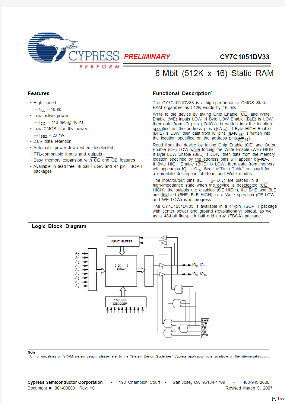
Write to the device by taking Chip Enable (CE) and Write Enable (WE) inputs LOW. If Byte LOW Enable (BLE) is LOW,then data from IO pins (IO 0–IO 7), is written into the location specified on the address pins (A 0–A 18). If Byte HIGH Enable (BHE) is LOW, then data from IO pins (IO 8–IO 15) is written into the location specified on the address pins (A 0–A 18).
Read from the device by taking Chip Enable (CE) and Output Enable (OE) LOW while forcing the Write Enable (WE) HIGH.If Byte LOW Enable (BLE) is LOW, then data from the memory location specified by the address pins will appear on IO 0–IO 7.If Byte HIGH Enable (BHE) is LOW, then data from memory will appear on IO 8 to IO 15. See the “Truth Table” on page 8 for a complete description of Read and Write modes.
The input/output pins (IO 0–IO 15) are placed in a high-impedance state when the device is deselected (CE HIGH), the outputs are disabled (OE HIGH), the BHE and BLE are disabled (BHE, BLE HIGH), or a Write operation (CE LOW,and WE LOW) is in progress.
The CY7C1051DV33 is available in a 44-pin TSOP II package with center power and ground (revolutionary) pinout, as well as a 48-ball fine-pitch ball grid array (FBGA) package.
Note
1.For guidelines on SRAM system design, please refer to the “System Design Guidelines” Cypress application note, available on the internet at https://www.360docs.net/doc/27448303.html, .
1415Logic Block Diagram
A 1A 2A 3A 4A 5A 6A 7A 8
COLUMN DECODER
R O W D E C O D E R
S E N S E A M P S
INPUT BUFFER
512K × 16ARRAY
A 0A 11A 13A 12A A A 16A 17A 18
A 9A 10IO 0–IO 7OE IO 8–IO 15
CE WE BLE
BHE
PRELIMINARY CY7C1051DV33
Selection Guide
–10
Unit Maximum Access Time 10ns Maximum Operating Current 110mA Maximum CMOS Standby Current
20
mA
Pin Configurations [2]
48-ball Mini FBGA
WE V CC A 11
A 10
NC A 6A 0A 3CE IO 10IO 8IO 9A 4A 5IO 11IO 13IO 12IO 14IO 15V SS A 9
A 8
OE V SS A 7IO 0BHE NC A 17A 2A 1BLE V CC IO 2IO 1IO 3IO 4IO 5IO 6IO 7A 15A 14A 13A 12NC A 18
NC
326541D E B A C F G H
A 16(Top View)
TSOP II
WE 1234567891011143132363534333740393812134144434216152930V CC A 5A 6A 7A 8A 0
A 1OE V SS A 17IO 15A 2CE IO 2IO 0IO 1BHE A 3A 418172019IO 32728252622
2123
24V SS IO 6IO 4IO 5IO 7A 16A 15BLE V CC IO 14IO 13IO 12IO 11IO 10IO 9IO 8A 14A 13A 12A 11A 9
A 10
A 18(Top View)
Note
2.NC pins are not connected on the die
PRELIMINARY CY7C1051DV33
Maximum Ratings
(Exceeding the maximum ratings may impair the useful life of the device. These are for user guidelines, they are not tested.)Storage Temperature .................................–65°C to +150°C Ambient Temperature with
Power Applied.............................................–55°C to +125°C Supply Voltage on V CC to Relative GND [3]....–0.5V to +4.6V DC Voltage Applied to Outputs
in High-Z State [3]....................................–0.3V to V CC + 0.3V DC Input Voltage [3].................................–0.3V to V CC + 0.3V
Current into Outputs (LOW).........................................20 mA Static Discharge Voltage............................................>2001V (per MIL-STD-883, Method 3015)
Latch-up Current......................................................>200 mA
Operating Range
Range Ambient Temperature V CC Industrial
–40°C to +85°C
3.3V ± 0.3V
DC Electrical Characteristics Over the Operating Range
Parameter Description
Test Conditions
–10Unit Min Max
V OH Output HIGH Voltage V CC = Min, I OH = –4.0 mA 2.4
V V OL Output LOW Voltage V CC = Min, I OL = 8.0 mA
0.4V V IH Input HIGH Voltage 2.0V CC + 0.3
V V IL [3]Input LOW Voltage –0.30.8V I IX Input Leakage Current GND < V I < V CC
–1+1μA I OZ Output Leakage Current GND < V OUT < V CC , Output Disabled –1
+1μA I CC
V CC Operating Supply Current
V CC = Max, f = f MAX = 1/t RC
100 MHz 110mA
83 MHz 100 66 MHz 9040 MHz
80I SB1Automatic CE Power Down Current —TTL Inputs Max V CC , CE > V IH V IN > V IH or V IN < V IL , f = f MAX 40mA I SB2
Automatic CE Power Down Current —CMOS Inputs Max V CC , CE > V CC – 0.3V,V IN > V CC – 0.3V or V IN < 0.3V, f = 0
20
mA
Capacitance [4]
Parameter Description
Test Conditions
Max.Unit C IN Input Capacitance T A = 25°C, f = 1 MHz, V CC = 3.3V
12pF C OUT
IO Capacitance
12
pF
Notes
3.V IL (min) = –2.0V and V IH (max) = V CC + 2.0V for pulse durations of less than 20 ns.
4.Tested initially and after any design or process changes that may affect these parameters
Thermal Resistance [4]
Parameter
Description Test Conditions
FBGA Package
TSOP II Package
Unit ΘJA Thermal Resistance (Junction to Ambient)Still Air, soldered on a 3 × 4.5 inch, four-layer printed circuit board
28.3151.43°C/W ΘJC
Thermal Resistance (Junction to Case)
11.4
15.8
°C/W
PRELIMINARY
CY7C1051DV33
AC Test Loads and Waveforms [5]
AC Switching Characteristics [6] Over the Operating Range
Parameter
Description
–10
Unit
Min
Max
Read Cycle t power [7]V CC (typical) to the first access 100μs t RC Read Cycle Time 10
ns t AA Address to Data Valid
10
ns t OHA Data Hold from Address Change 3
ns t ACE CE LOW to Data Valid 10ns t DOE OE LOW to Data Valid 5
ns t LZOE OE LOW to Low-Z 0
ns t HZOE OE HIGH to High-Z [8, 9]5
ns t LZCE CE LOW to Low-Z [9]3
ns t HZCE CE HIGH to High-Z [8, 9]5
ns t PU CE LOW to Power Up 0
ns t PD CE HIGH to Power Down 10ns t DBE Byte Enable to Data Valid 5
ns t LZBE Byte Enable to Low-Z 0
ns t HZBE
Byte Disable to High-Z
6
ns
Notes
5.AC characteristics (except High-Z) are tested using the load conditions shown in Figure (a). High-Z characteristics are tested for all speeds using the test load
shown in Figure (c).
6.Test conditions assume signal transition time of 3 ns or less, timing reference levels of 1.5V, input pulse levels of 0 to 3.0V.
7.t POWER gives the minimum amount of time that the power supply should be at typical V CC values until the first memory access can be performed.
8.t HZOE , t HZCE , t HZBE and t HZWE are specified with a load capacitance of 5 pF as in part (d) of AC Test Loads.Transition is measured when the outputs enter a
high impedance state.
9.At any given temperature and voltage condition, t HZCE is less than t LZCE , t HZOE is less than t LZOE , t HZBE is less than t LZBE , and t HZWE is less than t LZWE for any
given device.
90%10%
3.0V
GND
90%10%
ALL INPUT PULSES * CAPACITIVE LOAD CONSISTS OF ALL COMPONENTS OF THE TEST ENVIRONMENT
Rise Time: 1 V/ns
Fall Time: 1 V/ns
30 pF*
OUTPUT
Z = 50Ω
50Ω
1.5V (a)
3.3V OUTPUT
5 pF
(c)
R 317Ω
R2351Ω
High-Z Characteristics
(b)
PRELIMINARY CY7C1051DV33
Data Retention Waveform
Write Cycle [10, 11]t WC Write Cycle Time 10ns t SCE CE LOW to Write End 7ns t AW Address Setup to Write End 7ns t HA Address Hold from Write End 0ns t SA Address Setup to Write Start 0ns t PWE WE Pulse Width 7ns t SD Data Setup to Write End 5ns t HD Data Hold from Write End 0ns t LZWE WE HIGH to Low-Z [9]3
ns t HZWE WE LOW to High-Z [8, 9]5
ns t BW
Byte Enable to End of Write
7ns
Data Retention Characteristics Over the Operating Range
Parameter Description
Conditions [12]
Min Max
Unit V DR V CC for Data Retention 2.0
V I CCDR Data Retention Current
V CC = V DR = 2.0V , CE > V CC – 0.3V , V IN > V CC – 0.3V or V IN < 0.3V
20
mA t CDR [4]Chip Deselect to Data Retention Time 0ns t R [13]
Operation Recovery Time
t RC
ns
AC Switching Characteristics [6] Over the Operating Range (continued)
Parameter
Description
–10
Unit
Min
Max
3.0V 3.0V t CDR
V DR > 2V
DATA RETENTION MODE
t R
CE
V CC Notes
10.The internal Write time of the memory is defined by the overlap of CE LOW, and WE LOW. CE and WE must be LOW to initiate a Write, and the transition of
either of these signals can terminate the Write. The input data setup and hold timing should be referenced to the leading edge of the signal that terminates the Write.
11.The minimum Write cycle time for Write Cycle No. 3 (WE controlled, OE LOW) is the sum of t HZWE and t SD .12.No inputs may exceed V CC + 0.3V
13.Full device operation requires linear V CC ramp from V DR to V CC (min) > 50 μs or stable at V CC (min) > 50 μs.
PRELIMINARY CY7C1051DV33
Switching Waveforms
Read Cycle No. 1[14, 15]
Read Cycle No. 2 (OE Controlled)[15, 16]
Notes
14.Device is continuously selected. OE, CE, BHE or BHE or both= V IL .15.WE is HIGH for Read cycle.
16.Address valid prior to or coincident with CE transition LOW.
PREVIOUS DATA VALID
DATA VALID
t RC
t AA
t OHA
ADDRESS
DATA OUT
50%
50%
DATA VALID
t RC
t ACE
t DOE t LZOE t LZCE t PU
HIGH IMPEDANCE
t HZOE
t HZBE
t PD
HIGH
OE CE
ICC ISB IMPEDANCE
ADDRESS
DATA OUT V CC SUPPLY t DBE t LZBE
t HZCE BHE,BLE
CURRENT
I CC
I SB
PRELIMINARY CY7C1051DV33
Write Cycle No. 1 (CE Controlled)[17, 18]
Write Cycle No. 2 (BLE or BHE Controlled)
Notes
17.Data I/O is high-impedance if OE or BHE or BLE or both = V IH .
18.If CE goes HIGH simultaneously with WE going HIGH, the output remains in a high-impedance state.
Switching Waveforms (continued)
t HD
t SD
t SCE
t SA t HA
t AW
t PWE
t WC
BW
DATAI/O
ADDRESS
CE
WE
BHE,BLE
t t HD
t SD
t BW
t SA t HA
t AW
t PWE
t WC
t SCE
DATAI/O
ADDRESS
BHE,BLE
WE
CE
PRELIMINARY CY7C1051DV33
Write Cycle No. 3 (WE Controlled, OE LOW)
Switching Waveforms (continued)
t HD
t SD
t SCE
t HA
t AW
t PWE
t WC
t BW
DATA I/O
ADDRESS
CE
WE
BHE,BLE
t SA
t LZWE
t HZWE
Truth Table
CE OE WE BLE BHE I/O 0–I/O 7I/O 8–I/O 15Mode
Power H X X X X High-Z High-Z Power-down Standby (I SB )L L H L L Data Out Data Out Read All Bits Active (I CC )L L H L H Data Out High-Z Read Lower Bits Only Active (I CC )L L H H L High-Z Data Out Read Upper Bits Only Active (I CC )L X L L L Data In Data In Write All Bits Active (I CC )L X L L H Data In High-Z Write Lower Bits Only Active (I CC )L X L H L High-Z Data In Write Upper Bits Only Active (I CC )L
H
H
X
X
High-Z
High-Z
Selected, Outputs Disabled
Active (I CC )
Ordering Information
Speed (ns)Ordering Code Package Diagram Package Type
Operating Range 10
CY7C1051DV33-10BAXI 51-8510648-ball FBGA (Pb-Free)Industrial
CY7C1051DV33-10ZSXI
51-85087
44-pin TSOP II (Pb-Free)
Please contact your local Cypress sales representative for availability of these parts.
PRELIMINARY CY7C1051DV33 Package Diagrams
PRELIMINARY CY7C1051DV33
Document #: 001-00063 Rev. *C Page 10 of 11
? Cypress Semiconductor Corporation, 2006-2007. The information contained herein is subject to change without notice. Cypress Semiconductor Corporation assumes no responsibility for the All products and company names mentioned in this document may be the trademarks of their respective holders.
Figure 2. 44-pin TSOP II (51-85087)
Package Diagrams (continued)
51-85087-*A
PRELIMINARY CY7C1051DV33
Document History Page
Document Title: CY7C1051DV33 8-Mbit (512K x 16) Static RAM
Document Number: 001-00063
REV.ECN NO.Issue Date Orig. of
Change Description of Change **342195See ECN PCI New Data Sheet
*A380574See ECN SYT Redefined I CC values for Com’l and Ind’l temperature ranges
I CC (Com’l):Changed from 110, 90 and 80 mA to 110, 100 and 95 mA for 8, 10
and 12 ns speed bins respectively
I CC (Ind’l): Changed from 110, 90 and 80 mA to 120, 110 and 105 mA for 8, 10
and 12 ns speed bins respectively
Changed the Capacitance values from 8 pF to 10 pF on Page # 3 *B485796See ECN NXR Changed address of Cypress Semiconductor Corporation on Page# 1 from
“3901 North First Street” to “198 Champion Court”
Removed -8 and -12 Speed bins from product offering,
Removed Commercial Operating Range option,
Modified Maximum Ratings for DC input voltage from -0.5V to -0.3V and
V CC + 0.5V to V CC + 0.3V
Changed the Description of I IX from Input Load Current to
Input Leakage Current.
Changed t HZBE from 5 ns to 6 ns
Updated footnote #7 on High-Z parameter measurement
Added footnote #11
Updated the Ordering Information table and Replaced Package Name column
with Package Diagram.
*C866000See ECN NXR Changed ball E3 from V SS to NC in FBGA pin configuration
This datasheet has been downloaded from:
https://www.360docs.net/doc/27448303.html,
Free Download
Daily Updated Database
100% Free Datasheet Search Site
100% Free IC Replacement Search Site
Convenient Electronic Dictionary
Fast Search System
https://www.360docs.net/doc/27448303.html,
All Datasheets Cannot Be Modified Without Permission
Copyright ? Each Manufacturing Company