LMX2354TMNOPB;LMX2354SLBXNOPB;LMX2354TMXNOPB;中文规格书,Datasheet资料
LMX2354
LMX2354 PLLatinum Fractional N RF/ Integer N IF Dual Low Power Frequency Synthesizer LMX2354 2.5 GHz/550 MHz
Literature Number: SNAS118B
LMX2354
PLLatinum Fractional N RF/Integer N IF Dual Low Power Frequency Synthesizer LMX23542.5GHz/550MHz
General Description
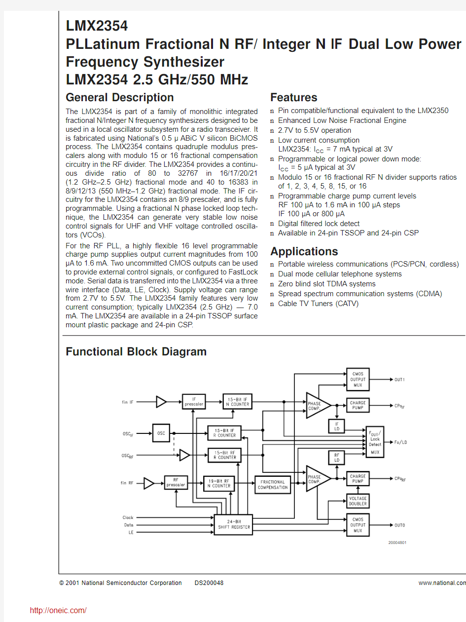
The LMX2354is part of a family of monolithic integrated fractional N/Integer N frequency synthesizers designed to be used in a local oscillator subsystem for a radio transceiver.It is fabricated using National’s 0.5μABiC V silicon BiCMOS process.The LMX2354contains quadruple modulus pres-calers along with modulo 15or 16fractional compensation circuitry in the RF divider.The LMX2354provides a continu-ous divide ratio of 80to 32767in 16/17/20/21(1.2GHz–2.5GHz)fractional mode and 40to 16383in 8/9/12/13(550MHz–1.2GHz)fractional mode.The IF cir-cuitry for the LMX2354contains an 8/9prescaler,and is fully https://www.360docs.net/doc/6b16224564.html,ing a fractional N phase locked loop tech-nique,the LMX2354can generate very stable low noise control signals for UHF and VHF voltage controlled oscilla-tors (VCOs).
For the RF PLL,a highly flexible 16level programmable charge pump supplies output current magnitudes from 100μA to 1.6mA.Two uncommitted CMOS outputs can be used to provide external control signals,or configured to FastLock mode.Serial data is transferred into the LMX2354via a three wire interface (Data,LE,Clock).Supply voltage can range from 2.7V to 5.5V.The LMX2354family features very low current consumption;typically LMX2354(2.5GHz)—7.0mA.The LMX2354are available in a 24-pin TSSOP surface mount plastic package and 24-pin CSP .
Features
n Pin compatible/functional equivalent to the LMX2350n Enhanced Low Noise Fractional Engine n 2.7V to 5.5V operation n Low current consumption
LMX2354:I CC =7mA typical at 3V
n Programmable or logical power down mode:I CC =5μA typical at 3V
n Modulo 15or 16fractional RF N divider supports ratios of 1,2,3,4,5,8,15,or 16
n
Programmable charge pump current levels RF 100μA to 1.6mA in 100μA steps IF 100μA or 800μA
n Digital filtered lock detect
n
Available in 24-pin TSSOP and 24-pin CSP
Applications
n Portable wireless communications (PCS/PCN,cordless)n Dual mode cellular telephone systems n Zero blind slot TDMA systems
n Spread spectrum communication systems (CDMA)n
Cable TV Tuners (CATV)
Functional Block Diagram
20004801
?2001National Semiconductor Corporation https://www.360docs.net/doc/6b16224564.html,
20004802
Order Number LMX2354TM or LMX2355TM
See NS Package Number MTC24
20004822
Order Number LMX2354SLB or LMX2355SLB
See NS Package Number SLB
L
https://www.360docs.net/doc/6b16224564.html, 2
Pin No.for TSSOP Package Pin No.for
CSP
Package
Pin
Name I/O Description
124OUT0O Programmable CMOS output.Level of the output is controlled by IF_N[17]bit. 21V CC
RF
—RF PLL power supply voltage input.Must be equal to Vcc IF.May range from
2.7V to5.5V.Bypass capacitors should be placed as close as possible to this
pin and be connected directly to the ground plane.
32V P
RF —Power supply for RF charge pump.Must be≥V CC
RF
and V CC
IF
.
43CP o
RF
O RF charge pump output.Connected to a loop filter for driving the control input
of an external VCO.
54GND—Ground for RF PLL digital circuitry.
65fin RF I RF prescaler input.Small signal input from the VCO.
76fin RF I RF prescaler complimentary input.A bypass capacitor should be placed as
close as possible to this pin and be connected directly to the ground plane.
87GND—Ground for RF PLL analog circuitry.
98OSC RF I Dual mode oscillator output or RF R counter input.Has a V CC/2input threshold
when configured as an input and can be driven from an external CMOS or TTL
logic gate.
109OSC IF I Oscillator input which can be configured to drive both the IF and RF R counter
inputs or only the IF R counter depending on the state of the OSC
programming bit.(See functional description1.1and programming description
3.1.)
1110Fo/LD O Multiplexed output of N or R divider and RF/IF lock detect.CMOS output.(See
programming description3.1.5.)
1211RF_EN I RF PLL Enable.Powers down RF N and R counters,prescaler,and
TRI-STATE?charge pump output when LOW.Bringing RF_EN high powers up
RF PLL depending on the state of RF_CTL_WORD.(See functional description
1.9.)
1312IF_EN I IF PLL Enable.Powers down IF N and R counters,prescaler,and TRI-STATE
charge pump output when LOW.Bringing IF_EN high powers up IF PLL
depending on the state of IF_CTL_WORD.(See functional description1.9.) 1413CLOCK I High impedance CMOS Clock input.Data for the various counters is clocked
into the24-bit shift register on the rising edge.
1514DATA I Binary serial data input.Data entered MSB first.The last two bits are the
control bits.High impedance CMOS input.
1615LE I Load Enable high impedance CMOS input.Data stored in the shift registers is
loaded into one of the4internal latches when LE goes HIGH.(See functional
description1.7.)
1716GND—Ground for IF analog circuitry.
1817fin IF I IF prescaler complimentary input.A bypass capacitor should be placed as
close as possible to this pin and be connected directly to the ground plane. 1918fin IF I IF prescaler input.Small signal input from the VCO.
2019GND—Ground for IF digital circuitry.
2120CPo IF O IF charge pump output.For connection to a loop filter for driving the input of an
external VCO.
2221V PIF—Power supply for IF charge pump.Must be≥V CC
RF and V CC
IF
.
2322V CC
IF —IF power supply voltage input.Must be equal to V CC
RF
.Input may range from
2.7V to5.5V.Bypass capacitors should be placed as close as possible to this
pin and be connected directly to the ground plane.
2423OUT1O Programmable CMOS output.Level of the output is controlled by IF_N[18]bit.
https://www.360docs.net/doc/6b16224564.html,
3
Parameter Symbol
Value
U Min Typ Max
Power Supply Voltage V CC
RF
?0.3 6.5
V CC
IF
?0.3 6.5
Vp RF?0.3 6.5
Vp IF?0.3 6.5 Voltage on any pin with GND=0V Vi?0.3V CC+0.3 Storage Temperature Range Ts?65+150 Lead Temperature(Solder4sec.)T L+260 Recommended Operating Conditions
Parameter Symbol
Value
Un Min Typ Max
Power Supply Voltage V CC
RF
2.7 5.5
V CC
IF V CC
RF
V CC
RF
V pRF V CC 5.5
V pIF V CC 5.5
Operating Temperature T A?40+85?Note1:“Absolute Maximum Ratings”indicate limits beyond which damage to the device may occur.Operating Ratings indicate conditions for which the intended to be functional,but do not guarantee specific performance limits.For guaranteed specifications and test conditions,see the Electrical Characteris guaranteed specifications apply only for the test conditions listed.
Note2:This Device is a high performance RF integrated circuit with an ESD rating<2kV and is ESD sensitive.Handling and assembly of this device sho be done at ESD-free workstations.
Electrical Characteristics(V
cc RF =V cc
IF
=V P
RF
=V P
IF
=3.0V;?40?C All min/max specifications are guaranteed by design,or test,or statistical methods. Symbol Parameter Conditions Value Min Typ Max GENERAL I CC Power Supply Current RF and IF 6.08.5 IF Only 1.1 2.0 I CC-PWDN Power Down Current RF_EN=IF_EN=LOW2050 f in RF RF Operating Frequency0.5 2.5 f in IF IF Operating Frequency10550 f OSC Oscillator Frequency No load on OSC RF250 fφPhase Detector Frequency RF and IF10 Pf in RF RF Input Sensitivity V CC=3.0V?150 V CC=5.0V?100 Pf in IF IF Input Sensitivity 2.7V≤V CC≤5.5V?100 V OSC Oscillator Sensitivity OSC IF,OSC RF0.5V CC CHARGE PUMP ICPo-source RF RF Charge Pump Output Current(see Programming Description3.2.2)VCPo Vp/2,RF_CP_WORD= 0000 ?100 ICPo-sink RF VCPo=Vp/2,RF_CP_WORD= 0000 100 ICPo-source RF VCPo=Vp/2,RF_CP_WORD= 1111 ?1.6 ICPo-sink RF VCPo=Vp/2,RF_CP_WORD= 11111.6 L https://www.360docs.net/doc/6b16224564.html,4 Symbol Parameter Conditions Value Units Min Typ Max ICPo-source IF IF Charge Pump Output Current(see Programming Description3.1.4)VCPo=Vp/2,CP_GAIN_8=0?100μA ICPo-sink IF VCPo=Vp/2,CP_GAIN_8=0100μA ICPo-source IF VCPo=Vp/2,CP_GAIN_8=1?800μA ICPo-sink IF VCPo=Vp/2,CP_GAIN_8=1800μA ICPo-Tri Charge Pump TRI-STATE Current 0.5≤VCPo≤Vp?0.5 ?40?C ?2.5 2.5nA RF ICPo-sink vs.ICPo-source RF CP Sink vs.Source Mismatch VCPo=Vp/2T A=25?C RF ICPo=900μA?1.6mA 3.510% ICPo vs.VCPo CP Current vs.Voltage Variation 0.5≤VCPo≤Vp?0.5 T A=25?C RF ICPo 510% ICPo vs.T CP Current vs Temperature VCPo=Vp/2 ?40?C 8% V CP Charge Pump Output Voltage(RF only)2.7V≤V CC≤3.3V,Doubler Enabled 2*V CC ?0.5 V DIGITAL INTERFACE(DATA,CLK,LE,EN,FoLD) V IH High-level Input Voltage(Note3)0.8V CC V V IL Low-level Input Voltage(Note3)0.2V CC V I IL Low-level Input Current V IL=0,V CC=5.5V,(Note3)?1.0 1.0μA I IH High-level Input Current V IH=V CC=5.5V,(Note3)?1.0 1.0μA I IH Oscillator Input Current V IH=V CC=5.5V100μA I IL Oscillator Input Current V IL=0,V CC=5.5V?100μA V OH High-level Output Voltage I OH=?500μA V CC ?0.4 V V OL High-level Output Voltage I OL=500μA0.4V MICROWIRE TIMING t CS Data to Clock Setup Time See Data Input Timing50ns t CH Data to Clock Hold Time See Data Input Timing10ns t CWH Clock Pulse Width High See Data Input Timing50ns t CWL Clock Pulse Width Low See Data Input Timing50ns t ES Clock to Load Enable Set Up Time See Data Input Timing 50ns t EW Load Enable Pulse Width See Data Input Timing50ns Note3:except f IN,OSC IF and OSC RF https://www.360docs.net/doc/6b16224564.html, 5 20004823 I1=CP sink current at V Do=Vp??V I2=CP sink current at V Do=Vp/2 I3=CP sink current at V Do=?V I4=CP source current at V Do=Vp??V I5=CP source current at V Do=Vp/2 I6=CP source current at V Do=?V ?V=Voltage offset from positive and negative rails.Dependent on VCO tuning range relative to V CC and ground.Typical values are between0.5V and Note4:I Do vs V Do=Charge Pump Output Current magnitude variation vs Voltage=[1?2*{||1|?||3|}]/[1?2*{||1|+||3|}]*100%and[1?2*{||4|?||6|}]/[1?2 ||6|}]*100% Note5:I Do-sink vs I Do-source=Charge Pump Output Current Sink vs Source Mismatch=[||2|?||5|]/[1?2*{||2|+||5|}]*100% Note6:I Do vs T A=Charge Pump Output Current magnitude variation vs Temperature=[||2@temp|?||2@25?C|]/||2@25?C|*100%and[||5@temp 25?C|]/||5@25?C|*100% https://www.360docs.net/doc/6b16224564.html,6 20004824 Note:N =10,000R =50P =16 Note:Sensitivity limit is reached when the error of the divided RF output,F o LD,is ≥1Hz. Typical Performance Characteristics I CC vs V CC LMX2354 I CPO TRI-STATE vs CP O Voltage 2000482520004827 Charge Pump Current vs CP O Voltage RF_CP_WORD =0000and 0111 IF CP_GAIN_8=0and 1 Charge Pump Current vs CP O Voltage RF_CP_WORD =0011and 1111 2000482820004829 https://www.360docs.net/doc/6b16224564.html, 7 Sink vs Source Mismatch (See (Note 6)under Charge Pump Current Specification Definitions) RF Input Impedance V CC =2.7V to 5.5V,f IN =550MHz to 2.5GHz (f IN Capacitor =100pF) 20004830 IF Input Impedance V CC =2.7V to 5.5V,f IN =50MHz to 550MHz (f IN Capacitor =100pF) LMX2354RF Sensitivity vs Frequency 20004832 200 L https://www.360docs.net/doc/6b16224564.html, 8 IF Input Sensitivity vs Frequency Oscillator Input Sensitivity vs Frequency 20004836 20004835 9 https://www.360docs.net/doc/6b16224564.html, 分销商库存信息: NATIONAL-SEMICONDUCTOR LMX2354TM/NOPB LMX2354SLBX/NOPB LMX2354TMX/NOPB