SI6926ADQ_05中文资料
Si6926ADQ
Vishay Siliconix
New Product
Document Number: 72754S-40230—Rev. A, 16-Feb-04
https://www.360docs.net/doc/6f3971854.html,
1
Dual N-Channel 2.5-V (G-S) MOSFET
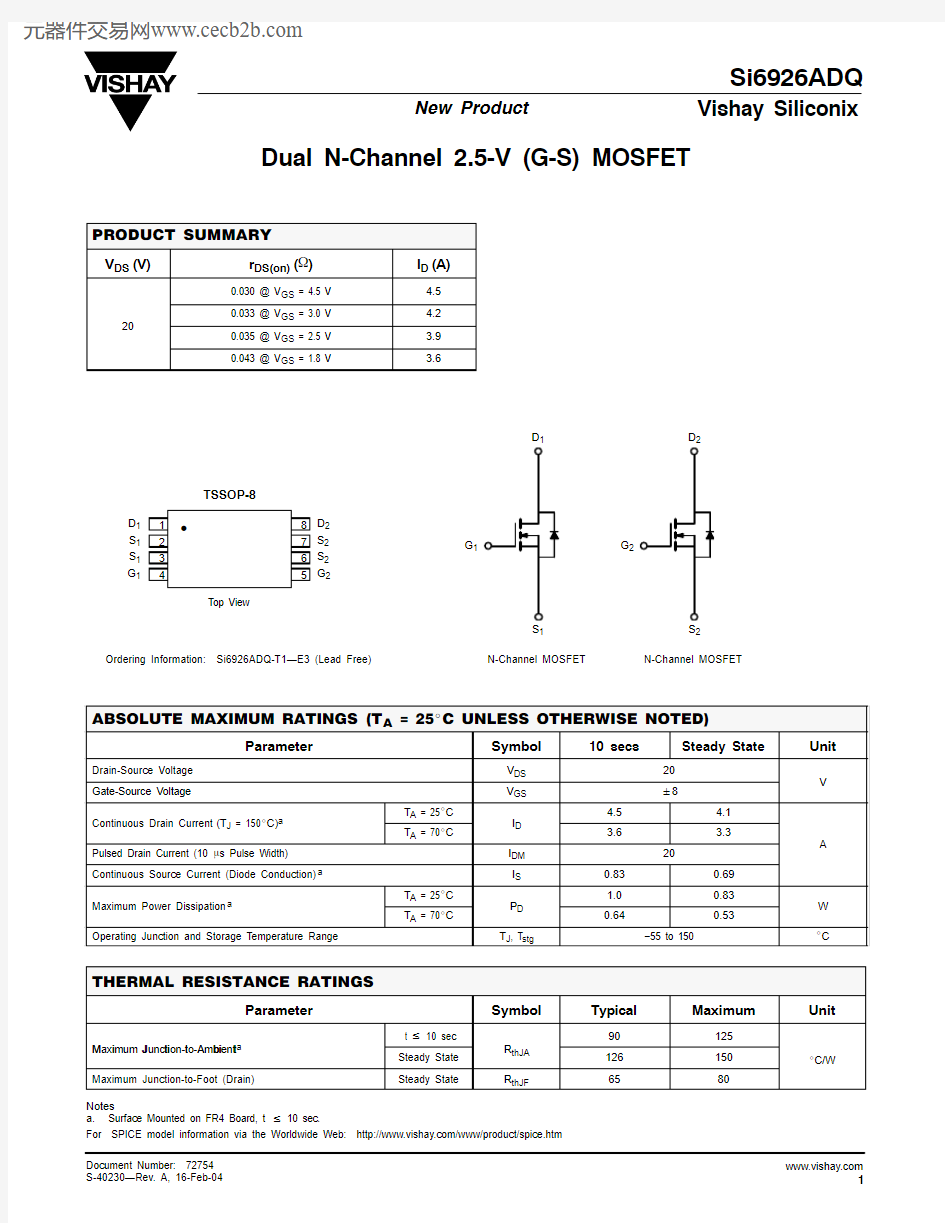
PRODUCT SUMMARY
V DS (V)
r DS(on) (W )
I D (A)
0.030 @ V GS = 4.5 V
4.50.033 @ V GS = 3.0 V 4.220
0.035 @ V GS = 2.5 V 3.90.043 @ V
GS = 1.8 V
3.6
D 1S 1S 1G 1
1234
8765D 2S 2S 2G 2
TSSOP-8
Top View
D
D G 11
N-Channel MOSFET
D G 2
2
N-Channel MOSFET
Ordering Information:Si6926ADQ-T1—E3 (Lead Free)
ABSOLUTE MAXIMUM RATINGS (T A = 25_C UNLESS OTHERWISE NOTED)
Parameter
Symbol
10 secs
Steady State Unit
Drain-Source Voltage V DS 20Gate-Source Voltage
V GS "8
V
T A = 25_C 4.5 4.1Continuous Drain Current (T J = 150_C)a T A = 70_C
I D 3.6
3.3
Pulsed Drain Current (10 m s Pulse Width)I DM 20
A
Continuous Source Current (Diode Conduction)a I S 0.830.69Maximum Power Dissipation T A = 25_C 1.00.83a
T A = 70_C P D 0.64
0.53
W Operating Junction and Storage Temperature Range
T J , T stg
?55 to 150
_C
THERMAL RESISTANCE RATINGS
Parameter
Symbol Typical
Maximum
Unit
M i
J ti t A bi t t v 10 sec 90125Maximum Junction-to-Ambient a Steady State R thJA 126150_Maximum Junction-to-Foot (Drain)
Steady State
R thJF
65
80
C/W
Notes
a.Surface Mounted on FR4 Board, t v 10 sec.
For SPICE model information via the Worldwide Web: https://www.360docs.net/doc/6f3971854.html,/www/product/spice.htm
Si6926ADQ
Vishay Siliconix
New Product
https://www.360docs.net/doc/6f3971854.html,
2
Document Number: 72754S-40230—Rev. A, 16-Feb-04
SPECIFICATIONS (T J = 25_C UNLESS OTHERWISE NOTED)
Parameter
Symbol Test Condition Min Typ a Max Unit
Static
Gate Threshold Voltage V GS(th)V DS = V GS , I D = 250 m A 0.40
1.0V Gate-Body Leakage
I GSS V DS = 0 V, V GS = "8 V "100nA V DS = 20 V, V GS = 0 V 1Zero Gate Voltage Drain Current I DSS V DS = 20 V, V GS = 0 V, T J = 55_C
5
m A On-State Drain Current
b
I D(on)
V DS w 5 V, V GS = 5 V 10
A
V GS = 4.5 V, I D = 4.5 A
0.0240.030V GS = 3.0 V, I D = 4.2 A 0.0260.033Drain-Source On-State Resistance b
r DS(on)
V GS = 2.5 V, I D = 3.9 A 0.0290.035W
V GS = 1.8 V, I D = 3.6 A
0.0350.043
Forward Transconductance b g fs V DS = 10 V, I D = 4.5 A 26S Diode Forward Voltage b
V SD
I S = 0.83 A, V GS = 0 V
0.6
1.1V Dynamic a
Total Gate Charge Q g 7.510.5
Gate-Source Charge Q gs V DS = 10 V, V GS = 4.5 V, I D = 4.5 A
1.2nC
Gate-Drain Charge Q gd 1.2Gate Resistance R g 1.9W
Turn-On Delay Time t d(on)612Rise Time
t r V 1625Turn-Off Delay Time t d(off)DD = 10 V, R L = 10 W
I D ^ 1 A, V GEN = 10 V, R g = 6 W 4670ns Fall Time
t f 915Source-Drain Reverse Recovery Time
t rr
I F = 0.83 A, di/dt = 100 A/m s 20
40
Notes
a.Guaranteed by design, not subject to production testing.
b.Pulse test; pulse width v 300 m s, duty cycle v 2%.
0.00
0.250.500.75
1.00
1.25
1.50
1.75
2.00
1
2
3
4
5
V DS ? Drain-to-Source Voltage (V)
V GS ? Gate-to-Source Voltage (V)
Si6926ADQ
Vishay Siliconix
New Product
Document Number: 72754S-40230—Rev. A, 16-Feb-04
https://www.360docs.net/doc/6f3971854.html,
3
TYPICAL CHARACTERISTICS (25_C UNLESS NOTED)
0.0
0.2
0.4
0.6
0.8
1.0
1.2
2004006008001000
120004
8
12
16
20
? O n -R e s i s t a n c e (r D S (o n )W )
0.60.8
1.0
1.2
1.4
1.6
?50
?250255075100125150
0123456
2
4
6
8
10
0.00
0.01
0.02
0.03
0.04
0.05
0.0
4.0
8.0
12.0
16.0
20.0
V
DS ? Drain-to-Source Voltage (V)
I
D ? Drain Current (A)Gate Charge
On-Resistance vs. Drain Current
? G a t e -t o -S o u r c e V o l t a g e (V )
Q g ? Total Gate Charge (nC)
C ? C a p a c i t a n c e (p F )
V G S Capacitance
On-Resistance vs. Junction Temperature
0.00
0.010.020.030.040.050.060.07
0.080
12345678
20
10
1Source-Drain Diode Forward Voltage
? O n -R e s i s t a n c e (r D S (o n )W )
V SD ? Source-to-Drain Voltage (V)V GS ? Gate-to-Source Voltage (V)
? S o u r c e C u r r e n t (A )
I S r D S (o n ) ? O n -R e s i i s t a n c e (N o r m a l i z e d )
https://www.360docs.net/doc/6f3971854.html, 4
Document Number: 72754
S-40230—Rev. A, 16-Feb-04 Single Pulse Power, Junction-to-Ambient
600
100
Si6926ADQ
Vishay Siliconix
New Product
Document Number: 72754S-40230—Rev. A, 16-Feb-04
https://www.360docs.net/doc/6f3971854.html,
5
TYPICAL CHARACTERISTICS (25_C UNLESS NOTED)
21
0.1
0.01
Normalized Thermal Transient Impedance, Junction-to-Foot
N o r m a l i z e d E f f e c t i v e T r a n s i e n t T h e r m a l I m p e d a n c e
Legal Disclaimer Notice
Vishay Document Number: https://www.360docs.net/doc/6f3971854.html, Revision: 08-Apr-051
Notice
Specifications of the products displayed herein are subject to change without notice. Vishay Intertechnology, Inc., or anyone on its behalf, assumes no responsibility or liability for any errors or inaccuracies.
Information contained herein is intended to provide a product description only. No license, express or implied, by estoppel or otherwise, to any intellectual property rights is granted by this document. Except as provided in Vishay's terms and conditions of sale for such products, Vishay assumes no liability whatsoever, and disclaims any express or implied warranty, relating to sale and/or use of Vishay products including liability or warranties relating to fitness for a particular purpose, merchantability, or infringement of any patent, copyright, or other intellectual property right. The products shown herein are not designed for use in medical, life-saving, or life-sustaining applications. Customers using or selling these products for use in such applications do so at their own risk and agree to fully indemnify Vishay for any damages resulting from such improper use or sale.