MT29F16G08CBACA__L72A 美光芯片
NAND Flash Die
16Gb Die: x8 300mm MLC MT29F16G08CBACA MT29F16G08CBECB
Features
?Contact factory for part availability
?Open NAND Flash Interface (ONFI) 2.2-compliant1?Multiple-level cell (MLC) technology ?Organization
–Page size x8: 4320 bytes (4096 + 224 bytes)
–Block size: 256 pages (1024K + 56K bytes)
–Plane size: 2 planes x 1024 blocks per plane
–Device size: 16Gb: 2048 blocks
?Synchronous I/O performance
–Up to synchronous timing mode 5
–Clock rate: 10ns (DDR)
–Read/write throughput per pin: 200MT/s ?Asynchronous I/O performance
–Up to asynchronous timing mode 5
–t RC/t WC: 20ns (MIN)
?Array performance
–Read page: 75μs (MAX)
–Program page: 1300μs (TYP)
–Erase block: 3ms (TYP)
?Operating Voltage Range
–V CC: 2.7–3.6V
–V CCQ: 1.7-1.95V, 2.7–3.6V
?Command set: ONFI NAND Flash Protocol ?Advanced Command Set
–Program cache
–Read cache sequential
–Read cache random
–One-time programmable (OTP) mode
–Multi-plane commands
–Multi-LUN operations
–Read unique ID
–Copyback
?First block (block address 00h) is valid when ship-ped from factory2
?RESET (FFh) required as first command after power-on
?Operation status byte provides software method for detecting:
–Operation completion
–Pass/fail condition
–Write-protect status ?Data strobe (DQS) signals provide a hardware meth-od for synchronizing data DQ in the synchronous interface
?Copyback operations supported within the plane from which data is read
?Operating temperature:
–Commercial: 0oC to +70oC
Die Outline
?Die size (stepping distance): 6.43380mm x
8.83905mm
?Bond pad location and identification, see Bond Pad Locations and Identification (page 5)
General Physical Specifications ?Nominal wafer thickness: 790μm ±25μm
?Typical bond-pad metal thickness: 17.7k??Typical topside passivation: 4k? oxynitride over 10.5k? of silane oxide
?Metallization composition: 3k? Pd over 10k? Ni over 3k? Cu
Options Marking Interface:
–Asynchronous MT29F16G08CBACA –Synchronous MT29F16G08CBECB ?Form: Wafer3W ?Testing: Standard probe C1
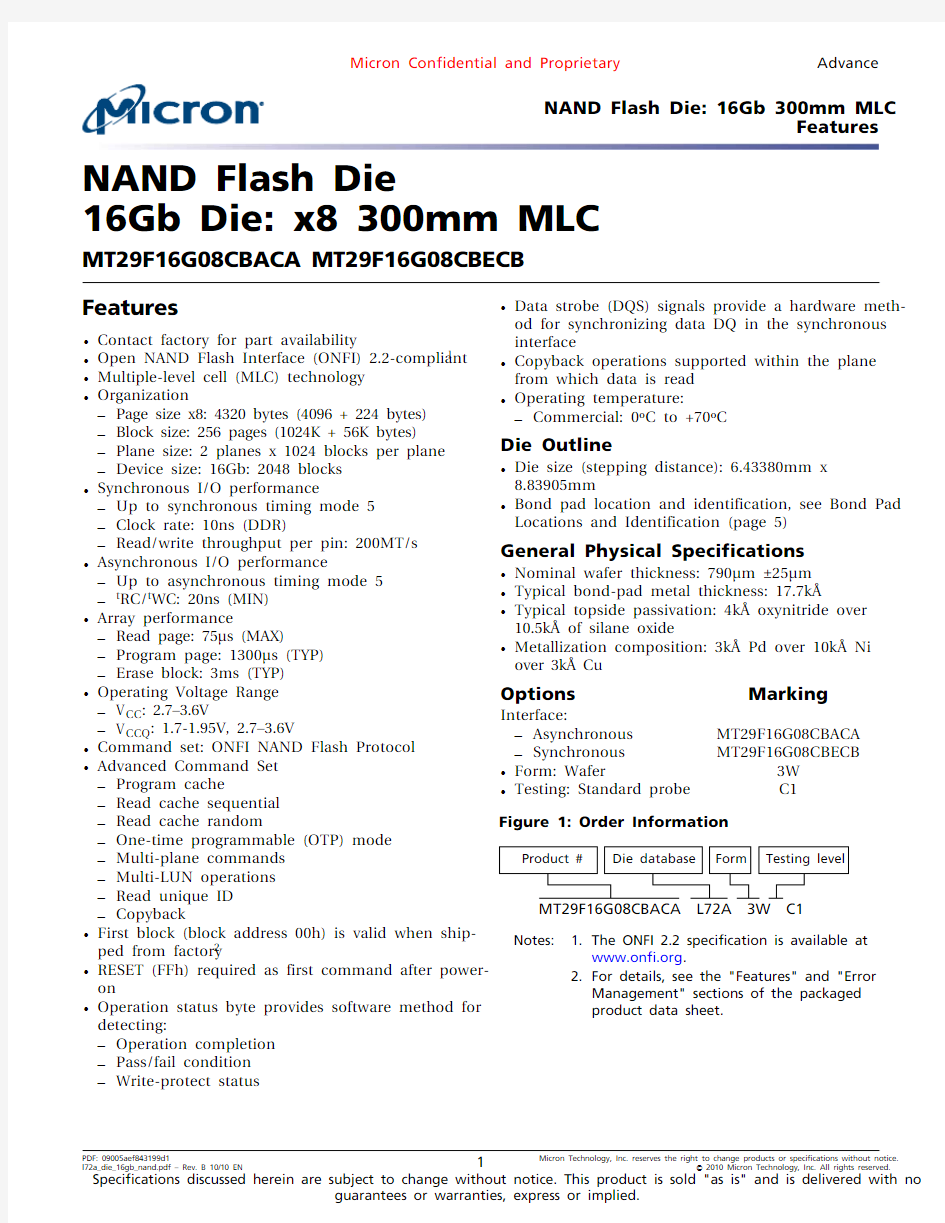
Figure 1: Order Information
MT29F16G08CBACA L72A 3W C1
Product #Die database Form Testing level
Notes: 1.The ONFI 2.2 specification is available at
https://www.360docs.net/doc/7f17443066.html,.
2.For details, see the "Features" and "Error
Management" sections of the packaged
product data sheet.
General Die Instructions
Die Testing Procedures
Micron? wafer products are tested at a standard probe test level. Wafer probe is per-
formed at an elevated temperature to ensure product functionality in Micron's stand-
ard packages. The package environment is not within Micron's control, so the user
must determine the necessary heat sink requirements to ensure that the die junction
temperature remains within specified limits.
Wafer-Level Testing
The standard probe flow is the same probe flow used for Micron's package products.
The following list provides an example of a standard probe test performed at wafer level
for Micron's products:
?Opens/shorts
?Input/output leakage tests
?I CC standby
?Voltage regulator performance
?Nominal V CC and V CCQ functional
?Memory array algorithmic patterns
?High voltage stress
?PROGRAM performance
?ERASE performance
?Invalid block marking
Repairs are implemented at each repair test. Repairable die are processed through re-
pair algorithms based on the repair solutions defined during the tests described above.
Post-repair testing is conducted with appropriate guardbands to ensure a consistently
high quality level.
The status register reports the status of die operations.
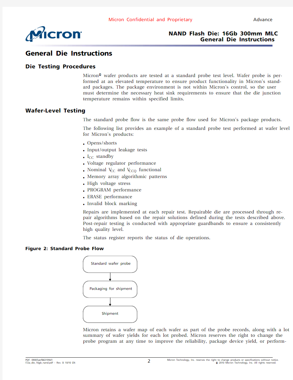
Figure 2: Standard Probe Flow
Micron retains a wafer map of each wafer as part of the probe records, along with a lot
summary of wafer yields for each lot probed. Micron reserves the right to change the
probe program at any time to improve the reliability, package device yield, or perform-
ance of the product. Die users may experience differences in performance and reliabili-
ty relative to Micron data sheet specifications. This is due to differences in package
capacitance, inductance, resistance, trace length, and device testing.
Functional Specification
The specifications in this die data sheet are provided for reference only. For target func-
tional and parametric specifications, refer to the packaged product data sheet. This
data sheet is available to customers under NDA; to obtain a copy, contact Micron
NAND Flash support at nandsupport@https://www.360docs.net/doc/7f17443066.html,.
Bonding Instructions
Refer to the Bond Pad Location from Pad 1 Center Table for a complete list of bond
pads and coordinates from bond pad 1 center, and to the Bond Pad Location from Die
Center Table for bond pad locations from center of die.
The back side of the die is at V SS potential. For improved thermal performance, it is rec-
ommended that the die be connected to the ground plane. It is also possible to leave
the back side of the die floating.
Micron recommends following the best practices guidelines (defined in the technical
note TN-29-24, "Micron Wire-Bonding Techniques," located on Micron's secure Web
site) when bonding to copper wafers with nickel-palladium metallization.
Wafer-Level Processing
Micron provides full-thickness wafers to accommodate post-processing. Post-process-
ing includes adding extra passivation or metal layers, or bumping bond-pads. The
street width is provided in the die outline, which also provides a reference from the cen-
ter of bond pad 1 to the center of the intersection of the two streets for easy alignment. Storage Requirements
Micron's wafer products are packaged for shipping in a cleanroom environment. Upon
receipt, the customer should transfer the die or wafers to a similar environment for stor-
age. Micron advises that customers avoid exposing Flash die products to ultraviolet
light or processing them at temperatures greater than 250°C for more than five minutes.
Failure to adhere to these handling instructions will result in irreparable damage to the
devices.
Micron also recommends that the wafers be maintained in a filtered nitrogen atmos-
phere until removed for assembly. The moisture content of the storage facility should
be maintained at 30% ±10% relative humidity. Precautions for avoiding ESD damage
are necessary during handling. The die must be in an ESD-protected environment for
inspection and assembly at all times.
Product Reliability Monitors
Micron’s QRA department continually samples product families for reliability studies.
These samples are subjected to a battery of tests known as "accelerated life and environ-
mental stress tests." During these tests, devices are stressed for many hours under
conditions designed to simulate years of normal field use. A summary of these product-
family evaluations is published on a regular basis and is available upon request.
Die/Wafer-Level Reliability and Screening
Extensive Micron qualification of both the die and the die manufacturing process
shows that production burn-in is not required to meet the endurance and data reten-
tion specifications on Flash products. Additional information is available upon request.
Bond Pad Locations and Identification
Bond pad locations are provided from the center of pad 1, located in the upper-left cor-
ner of the die (see Table 1), and from the center of the die (see Table 2).
Table 1: Bond Pad Location from Pad 1 Center
Notes: 1.Reference is to center of each bond pad from center of pad 1.
2.All die V CC and V SS pads must have separate connections.
3.DNU = do not use.
4.See Multiple-Die Stack Configurations (page 7) for bonding configuration.
5.For MT29F16G08CBACA this pad is DNU; for MT29F16G08CBECB connect to DQS.
Table 2: Bond Pad Location from Die Center
Notes: 1.Reference is to center of each bond pad from center of die.
2.All die V CC and V SS pads must have separate connections.
3.DNU = do not use.
4.See Multiple-Die Stack Configurations (page 7) for bonding configuration.
5.For MT29F16G08CBACA this pad is DNU; for MT29F16G08CBECB connect to DQS.
Multiple-Die Stack Configurations
More than one NAND die can be stacked into a package. It is possible for two die to
share a single CE# signal. When two die are connected to a single CE#, this permits Multi-LUN operations.
The multiple-die stack (MDS) bond pads are used to configure the NAND die to share a single CE#.
Table 3: MDS Bonding Configuration
Note:
1.DNU = do not use.
NAND Flash Die: 16Gb 300mm MLC Multiple-Die Stack Configurations
Device and Array Organization for Multiple-Die Stack Configurations
Figure 3: Example Device Organization for Single-Die Package
Async Sync CE# CE#CLE CLE ALE ALE WE# CLK RE# W/R#DQ[7:0] DQ[7:0]
N/A DQS WP#
WP#
R/B#
Note: 1.DNU = do not use.
Figure 4: Example Device Organization for Two-Die Package with Single CE#, Single I/O Channel
Async Sync CE# CE#CLE CLE ALE ALE WE# CLK RE# W/R#DQ[7:0] DQ[7:0]
N/A DQS WP#
WP#
R/B#
Note: 1.DNU = do not use.
Figure 5: Example Device Organization for Two-Die Package with Two CE#s, Two I/O Channels
CE#CLE-1ALE-1CLK-1W/R#-1DQ[7:0]-1DQS-1WP#-1
R/B#
CE2#CLE-2ALE-2CLK-2W/R#-2DQ[7:0]-2
DQS-2WP#-2
CE#CLE-1ALE-1WE#-1RE#-1DQ[7:0]-1
N/A WP#-1
CE2#CLE-2ALE-2WE#-2RE#-2DQ[7:0]-2
N/A WP#-2
R/B2#
Async Sync Note: 1.DNU = do not use.
Figure 6: Example Device Organization for a Four-Die Package with Two CE#s, Single I/O Channel
CE#
CLE
ALE
CLK W/R# DQ[7:0]
DQS
WP#
R/B#
CLE
ALE
CLK
W/R# DQ[7:0]
DQS
WP#R/B2#
CE#
CLE
ALE
WE#
RE#
DQ[7:0]
N/A
WP#
CE2#
CLE
ALE
WE#
RE#
DQ[7:0]
N/A
WP#
Async Sync
Note: 1.DNU = do not use.
Figure 7: Array Organization per Logical Unit (LUN)
(0, 2, 4, ..., 2046)(1, 3, 5, ..., 2047)
4320 bytes
Logical Unit (LUN)
Table 4: Array Addressing for Logical Unit (LUN)
Notes:
1.CAx = column address, PAx = page address, BAx = block address, LAx = LUN address; the
page address, block address, and LUN address are collectively called the row address.2.When using the synchronous interface, CA0 is forced to 0 internally; one data cycle al-ways returns one even byte and one odd byte.
3.Column addresses 4320 (10E0h) through 8191 (1FFFh) are invalid, out of bounds, do not
exist in the device, and cannot be addressed.4.BA[8] is the plane-select bit:
Plane 0: BA[8] = 0Plane 1: BA[8] = 1
https://www.360docs.net/doc/7f17443066.html,0 is the LUN-select bit. It is present only when two LUNs are shared on the target;
otherwise, it should be held LOW.LUN 0: LA0 = 0LUN 1: LA0 = 1
Identification Operations for Multiple-Die Stack Configurations
The data returned by the READ ID (90h) and READ PARAMETER PAGE (ECh) com-
mands are different depending on the MDS configuration (see Multiple-Die Stack
Configurations (page 7)).
Table 5: READ ID Parameters for Address 00h
Note: 1.h = hexadecimal.
Table 6: READ ID Parameters for Address 20h
Notes: 1.h = hexadecimal.
2.XXh = undefined.
Table 7: Parameter Page Data Structure Table
Table 7: Parameter Page Data Structure Table (Continued)
Table 7: Parameter Page Data Structure Table (Continued)
Table 7: Parameter Page Data Structure Table (Continued)
Table 7: Parameter Page Data Structure Table (Continued)
Table 7: Parameter Page Data Structure Table (Continued)
Table 7: Parameter Page Data Structure Table (Continued)
Die Features and Physical Specifications
Figure 8: L72A Die Outline
Note: 1.Die is not drawn to scale. Dimension are shown in Die Features and Physical Specifica-
tions (page 19)
Table 8: Die Dimensions
Table 8: Die Dimensions (Continued)
adobe 系列产品简介
给新手的Adobe软件不完全科普指南! /2015/03-20/200823.html @藻哲:Adobe的软件是大家日常使用频率非常高的软件,Adobe旗下都有些什么软件,这些东西是拿来干嘛的?对你的工作也没有帮助?今天就给各位简(话)略(唠)的说明一下!内含各种小技能小知识>>> 文章为个人见解(上班码字QAQ),欢迎交流,拒绝“友军之围”。文章偏长且经常跑题,建议收藏后慢慢吐槽。 首先,在开始之前回答两个重心问题: Q:我要不要买正版? A:2014年10月,Adobe属于中国的研发团队逐步解散,中国区的研发工作将交予Adobe印度公司负责。 大意就是,Adobe退出中国。想要了解的可以百度一下,有非常多的分析文章,我总结一下:Adobe在中国赚不到钱不单单是因为个人使用盗版,更是因为包括大企业和政府机关都会使用盗版(外国也是如此),重点是Adobe对中国市场的定位太高!价格贵得飞起且变动不灵活。(额,跑题了…)所以,你可以登录Adobe中国官网看看,现在最新的版本是CS6!而且价格是定死的!你可以再去Adobe香港看看,软件都是最新的,还可轻松登录云系统!软件也有多种套餐和优惠。所以即使你需要购买正版,也不要购买中国地区的。(个人见解,请勿随意参考) Q:盗版跟正版功能上有什么区别? A:这个问题挺多人问的,答案是:没有区别!有的同学发现自己安装的盗版有些功能不能用(比如PS的3D)其实是因为安装出错或者缺少需要的插件,建议下载大师版安装。Adobe的产品非常良心,导致盗版可以使用正版的全部功能,包括云系统!!!你完全可以使用盗版的云同步(感动得我合不拢腿)【给各位介绍一下这个非常神的功能,登录Creative Cloud后可以上传个人预设跟软件设置,特别是PS和AI,可以上传图层,比如你要把PSD 中某个元素发给同事改改,你们可以登录同一个账号,按一个按钮,你的PS图层就会出现在他的电脑AI上,完全不需要其他操作…】极其建议Adobe公司建立一个官方支付宝账号,方便被感动的人们自愿捐赠!(网络因人而异,有些版本或者地区可能会使用不了这个功能) 好的,= =,终于要开始正文了,本文完全没有鼓励大家使用盗版的意思,请各位也勿围绕盗版展开讨论。以下软件排名为乱序: Photoshop 说到PS,这玩意就是Adobe的发家致富之物,在很久很久之前,星球大战的特效师约翰·诺尔和他的弟弟在一个黑暗的房…停停停,不能扯历史了QAQ。各位感兴趣的可以自己上维基百科查看… PS就是一个图片处理软件,这个应该是不用介绍的,因为PS已经成为了一切修改图片的代言(曾经有师妹问我:师兄你是用什么软件PS的?)PS是一直领跑全球的图片处理软件,没有之一。
烽火系列产品介绍
Citrans 750城域骨干及汇聚节点 Citrans 750为标准型10G MSTP设备,提供强大的组网能力,可靠性设计完善,多业务接 口丰富,提供灵活的高阶/低阶业务调度和接入能力,是目前获得广泛商用的骨干或大型城 域网的汇聚层MSTP节点设备。 产品特点 组网能力强 Citrans 750支持多达6×10G的线路接口,同时支持最多16个 1+1/1:1/2BLSR保护的STM-1/4分支链/环,组网能力强大,适 合在复杂的网络环境下构建骨干层传输平台。 优化的多业务承载 Citrans 750除支持传统语音业务外,还支持10M/100Mb/s/1000Mb/s全速率的以太网业务,ATM业务;支持以太网业务的透传、交换、汇聚功能,支持GFP/LAPS/PPP封装、虚级联、LCAS、VLAN、STP、RPR、MPLS、ATM业务的统计复用等功能极大优化了数据业务的处理。将MSTP统一传输平台的技术优势发挥到淋漓尽致,最大限度地降低了建设和运营成本。 支持灵活的低阶业务接口 Citrans 750能够根据用户需要灵活配置低阶业务的交叉和接口模块,支持2M业务直接上下,相比于传统的采用低速率设备转接的方式,具有低成本、高可靠性、便于管理等等一系列突出优势。 槽位丰富,扩展性好 Citrans 750的槽位数量丰富,且各种业务接口完全通用,能够轻松适应网络结构的调整和业务扩展、升级带来的挑战。 高可用性设计 Citrans 750继承了烽火通信传统设备的高可用特性,在设备级提供重要部件的1+1备份;分散式电源供电,背板双电源接入,单盘双电源保护。网络级提供通道保护、复用段保护、子网连接保护等完善的保护措施,为您的网络提供高度可用性。 纳入OTNM2000/2100统一管理
电机系列产品介绍
Y系列(IP44)三相异步电动机(机座号80~355) 产品主要特点: Y系列(IP44)三相异步电动机(机座号80~355)系列标准化、系列化和通用化程度高,互换性好,体积小、重量轻,外形美观,效率、堵转转距、最大转距等性能指标均比JO2系列大大提高,其技术条件统一,易损件统一,外观基本统一,Y系列的安装尺寸及功率等级完全符合国际电工委员会(IEC)标准,并与德国 DIN42673标准相同,有利于配套和定购,也有利于在基本系列的基础上派生其他各种系列电机。 2008年本公司对Y系列进行了重新设计和改进,改进后其效率指标全部达到了GB 18613-2006《中小型三相异步电动机能效限定值及能效等级》的3级标准(等效于欧洲EFF2能效标准);符合IEC60034—2(1996)文件和国标《旋转电机(牵引电机除外)确定损耗和效率的试验方法》的要求,即B级绝缘电阻基准温度为95℃的规定。 主要技术参数: 额定频率为:50 Hz; 额定电压为:380 V; 外壳防护等级为:IP44; 冷却方法为:IC411; 结构及安装型式为:IM B3、IM B5、 IM B6、IM B7、IM B8、IM B35、IM V1、IM V3、IM V5、IM V6、IM V15和IM V36; 额定功率为:0.55 kW ,0.75 kW,1.1 kW,1.5 kW,2.2 kW,3 kW,4 kW,5.5 kW,7.5 kW,11 kW,15 kW,18.5 kW,22 kW,30 kW,37 kW,45 kW,55 kW,75 kW, 90 kW,110 kW,132 kW,160 kW (185 kW),200 kW(220 kW),250 kW,315 kW; 同步转速为:3000,1500,1000,750转/分,110Kw以上为3000,1500,1000,750,600转/分。 电动机的定额是以连续工作制(S1)为基准的连续定额。 功率在3 kW及以下者为Y接法,其它功率均为 接法。 主要应用场合: Y系列电动机为一般用途笼型三相异步电动机,可以用于启动性能,调速性
adobe 系列产品简介
给新手的Adobe软件不完全科普指南! https://www.360docs.net/doc/7f17443066.html,/edu/2015/03-20/200823.html @藻哲:Adobe的软件是大家日常使用频率非常高的软件,Adobe旗下都有些什么软件,这些东西是拿来干嘛的?对你的工作也没有帮助?今天就给各位简(话)略(唠)的说明一下!内含各种小技能小知识>>> 文章为个人见解(上班码字QAQ),欢迎交流,拒绝“友军之围”。文章偏长且经常跑题,建议收藏后慢慢吐槽。 首先,在开始之前回答两个重心问题: Q:我要不要买正版? A:2014年10月,Adobe属于中国的研发团队逐步解散,中国区的研发工作将交予Adobe印度公司负责。 大意就是,Adobe退出中国。想要了解的可以百度一下,有非常多的分析文章,我总结一下:Adobe在中国赚不到钱不单单是因为个人使用盗版,更是因为包括大企业和政府机关都会使用盗版(外国也是如此),重点是Adobe对中国市场的定位太高!价格贵得飞起且变动不灵活。(额,跑题了…)所以,你可以登录Adobe中国官网看看,现在最新的版本是CS6!而且价格是定死的!你可以再去Adobe香港看看,软件都是最新的,还可轻松登录云
系统!软件也有多种套餐和优惠。所以即使你需要购买正版,也不要购买中国地区的。(个人见解,请勿随意参考) Q:盗版跟正版功能上有什么区别? A:这个问题挺多人问的,答案是:没有区别!有的同学发现自己安装的盗版有些功能不能用(比如PS的3D)其实是因为安装出错或者缺少需要的插件,建议下载大师版安装。Adobe的产品非常良心,导致盗版可以使用正版的全部功能,包括云系统!!!你完全可以使用盗版的云同步(感动得我合不拢腿)【给各位介绍一下这个非常神的功能,登录Creative Cloud后可以上传个人预设跟软件设置,特别是PS和AI,可以上传图层,比如你要把PSD 中某个元素发给同事改改,你们可以登录同一个账号,按一个按钮,你的PS图层就会出现在他的电脑AI上,完全不需要其他操作…】极其建议Adobe公司建立一个官方支付宝账号,方便被感动的人们自愿捐赠!(网络因人而异,有些版本或者地区可能会使用不了这个功能) 好的,= =,终于要开始正文了,本文完全没有鼓励大家使用盗版的意思,请各位也勿围绕盗版展开讨论。以下软件排名为乱序:
伊利产品系列介绍
伊利系列产品 纯牛奶 类型规格及容量 伊利纯牛奶24*250ml 伊利纯牛奶6*1000ml 43.00元/箱 33.00元/箱 箱价产品诉求 早晨一杯天然,宣告活力百倍的一天开始。晚上一杯天然,是劳累一天的最好慰劳。和家人天天分享天然, 快乐、幸福、营养通通加倍没商量。我们的牛奶为什么天天天然的呢?大家都知道, 要孩子身心健康,就要让他在天然环境中均衡发展。我们为了产岀营养均衡的好奶,需要有均衡发展的奶 牛,因此,我们用培养孩子的观念养育奶牛。你看,在伊利天然牧场,那里有清新的空气,纯净、无污染的 泉水,种类繁多、且含有不同营养成分的天然牧草,奶牛们可以充分享受温暖的阳光,忘乎所以的互相嘻 闹,它们不但环境自在舒服,而且连它们每餐吃的,都是经过国家绿色食品发展中心认证的纯天然无污染的 绿色食品。它们有自己的名字、档案,还受到专职畜牧师和营养师的精心照顾,个个营养均衡、身心健康 哦!它们产岀的牛奶也与众不同,不但营养均衡,并且具有天然牛奶的独有香浓。为保证所产岀的牛奶保持 天然品质,牛奶的生产从奶牛乳房中挤岀的那一刻就在全封闭中,完全隔绝空气,并采用国际先进的全自 动、全封闭牛奶运输、生产灌装线,确保每一滴伊利牛奶原来的均衡营养不被破坏,是名副其实的天然牛 奶。
伊利低脂高钙奶24*250ml 50.00元/箱 伊利低脂高钙奶12*1000ml 70.00元/箱功 能 奶 伊利脱脂牛奶伊利脱脂牛奶伊利咖啡奶伊利草莓奶24*250ml 12*1000ml 24*250ml 50.00元/箱 70.00元/箱 40.00元/箱24*250ml 40.00元/箱 花 色 奶 伊利巧克力奶 富含天然乳钙的伊利高钙奶,是你最佳的钙源选择,因为这是从鲜牛奶中提取的乳钙,是一种具有良好感官特性 的新的天然钙源,它的含钙量较高,溶解性好,有良好的生物,利用度。在口味方面也比传统的钙制剂有了很大 的改善。最重要的是,由于乳钙是从天然牛奶中直接提取的,没有以往钙源所不可避免的副作用,其一升新鲜牛 奶所含活性钙约1250毫克,居众多食物之首,它 不但含量高,而且含VD3能促进人体肠壁对钙的吸收,吸收率高达98%,调节体内钙的代谢,维 持血清钙浓鸭,增进骨骼的钙化。就让我们用更多的热情投入到补钙运动中吧,从自己做起,从每天喝伊利高钙 奶始。 享尽纯牛奶的自然清新、天然香浓之际,是否又想在健康营养的前提下,尝尝更多的滋味,调 换调换多变的心情?天然和美味的绝配一一伊利的花色奶这时就是你的不二选择。伊利花色奶是 在草原鲜牛奶中添加适量的可饮用水、适量的稳定剂、香料、天然色素等添加剂制成,堪称香浓牛奶与鲜美口味的 完美组合,让你一口尝出缠绵在一起的两种味道。更有草莓味,巧克力味,咖啡味或甜味四种口味随意选择。草莓 奶酸甜爽口,新鲜诱人;咖啡奶馥郁浓香,回味悠长,巧克力奶幼滑浓郁,余香绵长;甜味奶柔和饱满,香甜入 心!每一口都能给你一个惊喜,一种满足,大饱口福之际,你会发现,快乐其实就是这么简单,又是这么丰富! 享尽纯牛奶的自然清新、天然香浓之际,是否又想在健康营养的前提下,尝尝更多的滋味,调 换调换多变的心情?天然和美味的绝配一一伊利的花色奶这时就是你的不二选择。伊利花色奶是 在草原鲜牛奶中添加适量的可饮用水、适量的稳定剂、香料、天然色素等添加剂制成,堪称香浓 牛奶与鲜美口味的完美组合,让你一口尝出缠绵在一起的两种味道。更有草莓味,巧克力味,咖 啡味或甜味四种口味随意选择。草莓奶酸甜爽口,新鲜诱人;咖啡奶馥郁浓香,回味悠长,巧克 大饱口福之际,你会发现,快乐其实就是这么简单,又是这么丰富! 力奶幼滑浓郁,余香绵长;甜味奶柔和饱满,香甜入心!每一口都能给你一个惊喜,一种满足, * 24*250ml 40.00元/箱
ibm全系列产品专题介绍
Systemx 产品概览
田晨
System x Technical Support Engineer Teamlead
AGENDA
Systemx 产品家族 海量服务器 企业级服务器 刀片服务器(Flex, BladeCenter) 高密度服务器(NextScale, iDataPlex) 网络交换机产品
2
Systemx 产品家族
New – completely refreshed, comprehensive portfolio
System x Innovation Heritage
X6
Flex System X6 System x3850 X6 System x3950 X6
iDataPlex
Flex System PureFlex
iDataPlex warm water cooling technology
2014 2013
BladeCenter eX5
2012
1997 - 2011
1st 1U form factor rack server – (1999) 1st scalable 16-socket X-Architecture (2002) 1st to market with blade servers (2002) Innovative iDataPlex – Dense (2008) Acquired Blade Network Technologies (2009) eX5 Launch –#1 market share (2010)
NeXtScale Dense Platform System x M4
4