CuInS2 Films for Photovoltaic Applications Deposited
CuInS2Films for Photovoltaic Applications Deposited by a
Low-Cost Method
T.Todorov,*,?E.Cordoncillo,?J.F.Sa′nchez-Royo,?J.Carda,?and P.Escribano?Departamento de Qu?′mica Inorga′nica y Orga′nica,Uni V ersidad Jaime I,12071Castello′n de la Plana, Spain,and Instituto de Ciencia de los Materiales,Uni V ersitat de Valencia,c/Dr.Moliner50,
46100Burjassot,Valencia,Spain
Recei V ed March20,2006
We report an atmospheric-pressure deposition method for preparing well-adhered and compact CuInS2 films.The precursor film is obtained by a solution-coating technique and is subjected to a low-cost and safe one-step reduction-sulfurization treatment.A maximum thickness of300nm is achieved per layer, and up to three layers were sulfurized at a time.The obtained films were characterized by X-ray diffraction (XRD),X-ray photoelectron spectroscopy(XPS),scanning electron microscopy(SEM)and visible-near-infrared(vis-NIR)spectrophotometry.
1.Introduction
If human civilization is to achieve sustainable develop-ment,it must urgently find a replacement for fossil fuels. The direct conversion of sunlight into electricity is a preferred method for clean and safe energy production in the future, and solar radiation is sufficiently abundant and widespread to satisfy society’s energy needs.Furthermore,photovoltaic installations are some of the most environmentally friendly and easily maintainable alternative energy converters.The main handicap to their widespread adoption is the high production price of the currently available photovoltaic modules based on crystalline silicon or vacuum-processed thin films.1,2New low-cost and easily scaled production technologies need to be developed before photovoltaics can contribute significantly to global energy production. Compound thin-film solar cell technologies are expected to lead to lower processing costs while maintaining high efficiency,making photovoltaics competitive with traditional means of energy production.In this sense,thin-film chal-copyrite solar cells are promising for future large-scale production.The high absorption coefficient and adequate band gap of these materials permits high efficiencies with relatively thin absorber layers.Highest theoretical efficiency (25%)3is attributed to CuInS2,although the experimental record(19.2%)has been achieved with CIGS[Cu(In,Ga)-(Se,S)2]absorbers.4Pilot plants for CIGS modules employing coevaporation5and rapid thermal treatment of stacked elemental layers6are already yielding stable production with considerable efficiency.Pilot facilities for CuInS2modules are being constructed as well.7Important cost reduction upon upscaling of these productions is envisioned,8although the necessary vacuum equipment would require large capital investments.
Although low-cost methods for chalcopyrite films deposi-tion have been reported,9they yield inferior film quality and cell performance.These methods include spray pyrolysis,10-13 electrodeposition,14,15and nanoparticle precursors.16-18Com-pact films have been obtained from ethylcellulose paste containing metal salts treated with elemental selenium vapor,16in this case forming an amorphous carbon under-layer.Relatively high efficiency(13.6%)has been obtained by printing suspensions of oxide nanoparticles followed by consecutive reduction and selenization with H2and H2Se.16 In most of these low-cost methods,problems with either layer adhesion or densification arise.Furthermore,the use of H2 and H2S or H2Se requires special safety precautions. Several reports describe the conversion of oxide precursors deposited by spray pyrolysis to chalcogenide films by direct treatment with chalcogen vapor,which can be considered safer and relatively environmentally friendly.CuInSe212,13
*Corresponding author:phone(+34)964728245;e-mail krassimi@qio.uji.es.?Universidad Jaime I.
?ICMUV.
(1)Surek,T.J.Cryst.Growth2005,275,292.
(2)Zweibel,K.Solar Energy Mater.Solar Cells2000,63,375.
(3)Siebentritt,S.Thin Solid Films2002,403,1.
(4)Ramanathan,K.;Contreras,M.;Perkins,C.;Asher,S.;Hasoon,F.;
Keane,J.;Young,D.;Romero,M.;Metzger,W.;Noufi,R.;Ward,J.;
Duda,A.Prog.Photo V oltaics Res.Appl.2003,11,225.
(5)Lammer,M.;Kniese,R.;Powalla,M.Thin Solid Films2004,451,
175.
(6)Palm,J.;Probst,V.;Karg,F.Solar Energy2004,77,757.
(7)Klenk,R.;Scheer,D.;Lux-Steiner,M.;Luck,I.;Meyer,N.;Ruhle,
U.Thin Solid Films2005,480,509.
(8)Powalla,M.;Dimmler,B.Thin Solid Films2000,361-362,540.
(9)Kaelin,M.;Rudmann,D.;Tiwari,A.Solar Energy2004,77,749.
(10)Oja,I.;Nanu,M.;Katerski,A.;Krunks,M.;Mere,A.;Raudoja,J.;
Goosens,A.Thin Solid Films2005,480-481,82.
(11)Hollingsworth,J.;Banger,K.;Jin,M.;Harris,J.;Cowen,J.;Bohannan,
E.;Switzer,J.;Buhro,W.;Hepp,A.Thin Solid Films2003,431-
432,63.
(12)Weng,S.;Cocivera,M.J.Appl.Phys.1993,74,2046.
(13)Beck,M.;Cocivera,M.Thin Solid Films1996,272,71.
(14)Taunier,S.;Grand,P.;Chomont,A.;Ramdani,O.;Naghavi,N.;
Hubert,C.;Mahe,E.;Kerrec,O.et al.Thin Solid Films2005,480-481,526.
(15)Bhattacharya,R.;Hiltner,J.;Batchelor,W.;Contreras,M.;Noufi,R.;
Sites,J.Thin Solid Films2000,361,396.
(16)Kaelin,M.;Rudmann,D.;Kurdesau,F.;Zogg,H.;Meyer,T.;Tiwari,
A.Thin Solid Films2005,480,486.
(17)Eberspacher,C.;Friedrich,C.;Pauls,K.;Serra,J.Thin Solid Films
2001,387,18.
(18)Kapur,V.;Bansal,A.;Asensio,I.Thin Solid Films2003,431,53.
3145
Chem.Mater.2006,18,3145-3150
10.1021/cm0606631CCC:$33.50?2006American Chemical Society
Published on Web06/03/2006
and CdS19were successfully obtained from oxide films without the use of additional reducing gases.
With some exceptions,10most of the low-cost approaches to absorber materials have been focused on selenide-based materials and their doping with elements such as Ga in order to tune the optical band gap to the optimal for solar energy conversion(1.5eV),which is inherent to pure CuInS2. This paper reports a low-cost and safe route for synthesiz-ing CuInS2films by use of amorphous oxide precursor film deposited by a soft-chemistry method.The substrates are
coated with triethanolamine-ethanol solutions of Cu(II)and In(III)acetates and subjected to a reduction-sulfurization treatment with ethanol-saturated nitrogen and elemental sulfur.
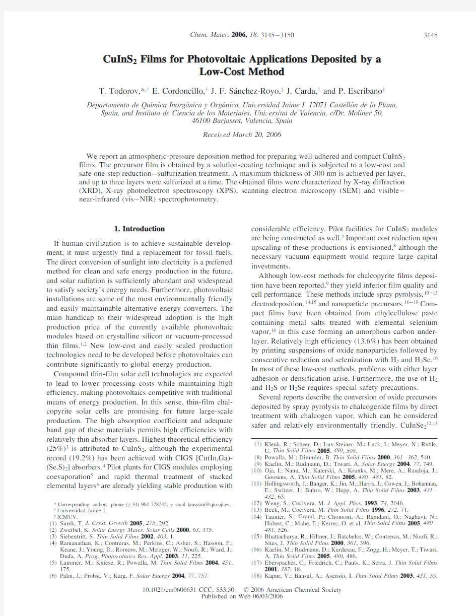
Previous work on soft-chemistry methods for copper-oxide film deposition reports the use of mono-and diethanolamine copper(II)acetate complexes.20While smaller crystal size was obtained with diethanolamine,the reasons for this were not discussed.Two possible explanations could be the better chelating ability of diethanolamine and the fact that the rate constant of the reduction of Cu(II)-amine complexes was found to increase in the order mono- To avoid a separate treatment and to favor the reduction reactions during the atmospheric pressure sulfurization process,we introduced ethanol vapor as a reducing agent in the N2carrier gas. The whole process is carried out at atmospheric pressure without the use of toxic or inflammable gases,thus reducing the health hazards as well as the materials and equipment costs.Although we have used the spin-coating technique, any standard coating method such as spraying,printing,or dipping can be used,achieving almost complete material utilization. 2.Experimental Section 2.1.Reagents.All reagents used for the deposition were analytical grade:copper(II)acetate monohydrate,Cu(CH3COO)2?H2O,(98%,Aldrich);indium(III)acetate,In(CH3COO)3,(99.99%, Aldrich);triethanolamine[tris-(2-hydroxyethyl)amine,TEA],(99%,Riedel-de Haen);ethanol,CH3CH2OH,(99.8%,Scharlau);sulfur, S(99.5%,J.P.Baker). 2.2.Preparation of the Coating Solution.Copper(II)acetate monohydrate and indium(III)acetate were dissolved into a TEA/ water/ethanol solution.The Cu:In:TEA:H2O:ethanol ratio was1:1: 5:4:26.The mixture was first stirred for4h at60°C and then for 24h at room temperature.The obtained transparent deep-blue solution was used directly(samples A and B)or diluted with ethanol to deposit thinner layers(sample D). 2.3.Film Deposition.Glass slides(Menzel-glaser)were used as substrates.Prior to deposition,the substrates were ultrasonically cleaned in a water-detergent solution and then washed with distilled deionized water and ethanol. The samples were spin-coated(Chemat Technology KW-4A coater)at2000rpm for1min,preceded by spin-up at500rpm for 2s.The obtained transparent films were heat-treated consecutively on two separate hot plates.The first one was maintained at250°C to eliminate the solvents and to initiate precursor decomposition, upon which the films turned reddish-brown.The second plate was adjusted by use of an infrared thermometer(Scantemp ST80XB) so that the surface of the films was maintained at350-360°C. During the5-min process,the samples turned transparent with a slightly brownish hue.The coating cycle was repeated1-3times for concentrated solutions(samples A1,2,3and B1,2,3,respectively) and8times for the solution diluted with an equal volume of ethanol (sample D). 2.4.Sulfurization.The samples were subjected to a novel one-step reduction-sulfurization process using ethanol-saturated nitro-gen gas and elemental sulfur.The reactor(Figure1)consisted of a50cm-long borosilicate glass tube inserted in a tubular oven.A glass bubbler filled with ethanol was connected to the inlet pipe. The sulfur source consisted of a smaller diameter15cm glass tube, whose position could be adjusted inside the wider tube.The outlet of the reactor was plugged with glass cotton.The hot gases that might otherwise corrode the metal parts of the oven were guided away through an exhaust tube made of aluminum foil on which most of the residual sulfur condensed.The treatments were performed under a fume hood. In a typical experiment,the source tube was loaded with2g of precipitated sulfur distributed along10cm and set at the beginning of the hot zone of the tubular oven.The samples were heated at a rate of20°C/min up to the maximum temperature s450°C for samples A,500°C for samples B,and550°C for samples C and D s in a flow of ethanol-saturated N2(about0.5L/min).During the heating,the material at the end of the sulfur source melted, initiating slow evaporation.Five minutes after the maximum temperature was reached,the sulfur source was moved manually about1cm at1-min intervals for10min into the hot zone.At the end of this intense sulfurization treatment,the reactor was withdrawn from the oven,letting the sulfur source cool for1min before removal of the samples from the hot zone. To study the reducing effect of ethanol,a three-layered sample was subjected to identical treatment at500°C in a clean glass tube without a sulfur source. (19)Weng,S.;Cocivera,M.Solar Energy Mater.Solar Cells1995,36, 301. (20)Oral,A.;Mensur,E.;Aslan,M.;Basaran,E.Mater.Chem.Phys.2004, 83,140. (21)Kumbhar,A.;Kishore,K.Radiat.Phys.Chem.2003,66,275. (22)Whitmire,K.;Hutchison,J.;Gardberg,A.;Edwards,C.Inorg.Chim. Acta1999,294,153. (23)Emons,T.;Li,J.;Nazar,L.J.Am.Chem.Soc.2002,124,8516. (24)Kirilov,A.;Kopylovich,M.;Kirilova,M.;Haukka,M.;Guedes da Silva,M.;Pombeiro,A.Angew.Chem.2005,117, 4419.Figure1.Experimental setup for the reduction-sulfurization process. 3146Chem.Mater.,Vol.18,No.13,2006Todoro V et al. The sulfurization treatment conditions of the films are sum-marized in Table1.The procedure was performed only once after the deposition of all precursor layers,except for sample E,which was sulfurized a total of three times after the deposition of each layer. 2.5.Characterization of the Films.The crystal structure of the films was monitored by X-ray powder diffraction(XRD)with a Siemens D5000D diffractometer equipped with a Cu K R radiation source and Siemens Diffract Plus software,which also determined diffraction peak positions and intensities.Data were collected by step-scanning from20°to60°2θwith a step size of0.05°2θand 1s counting time per step.The instrument was calibrated by use of an external Si standard,which served also as a reference for grain-size determination. The optical transmission of the films was measured with a Cary 500Scan UV-vis-NIR spectrophotometer.The data were regis-tered from400to1100nm with an uncoated glass as a reference. Film composition was studied by X-ray photoelectron spectros-copy(XPS)depth profiling.The measurements were carried out in an ultrahigh-vacuum evaporation chamber connected to an Escalab210multianalysis system(base pressure1.0×10-10mbar) from Thermo VG Scientific.Photoelectrons were excited with the Mg K R line(1253.6eV).The sample was successively sputtered by using an Ar ion gun until the film was removed from the sputtered area,allowing us to analyze the homogeneity of the sample. Film morphology and composition were determined by scanning electron microscopy(SEM)on a scanning electron microscope (Leica Leo440)equipped with a spectrometer for energy-dispersive X-ray microanalysis(EDX)under the following operating param-eters:acceleration voltage20kV,measuring time100s,working distance25mm,and counting rate1.2kcps.The samples for microstructure and microanalysis determination were introduced by use of an aluminum holder with graphite adhesive tape.The thickness of the films was estimated from micrographs of film cross sections. 3.Results and Discussion 3.1.X-ray Diffraction.The XRD of all films pretreated in air can be assigned to an amorphous material,although a small peak in the diffraction patterns of the reddish-brown samples obtained after the first firing at250°C could be attributed to elemental copper.This peak disappears as films turn transparent during the heat treatment at350°C. These results suggest that the reduction of Cu(II)to Cu(I) is initiated in the precursor solution as already mentioned in the Introduction.The oxidation of the organic material during the heat treatment leads to the reduction of copper to the elemental state at250°C that in the next firing at350°C generates amorphous material.The color change to transpar-ent with a very slight brownish hue suggests that the Cu(0) is oxidized to Cu(I).25Hence it can be concluded that prior to sulfurization the films are composed mainly of Cu(I)and In(III)amorphous oxides,although the presence of a small amount of Cu(II)cannot be excluded.12 The reducing effect of ethanol vapor during the next sulfurization step is demonstrated by repeating the treatment process at500°C,but in a flow of ethanol-saturated N2with no sulfur addition.The XRD results indicate the presence of metallic copper and In2O3. Thus it can be inferred that the proposed synthesis route can lead to the formation of Cu(I)through the reduction of Cu(II)complexes in solution,during the oxidation of the organic material and/or ethanol. Figure2presents the diffractograms of thin-film samples after sulfurization under different conditions.The diffraction data can be summarized as follows: The diffraction peaks can be assigned to the CuInS2 crystalline structure,space group I-42d,with a preferred (112)-plane orientation,according to the JCPDS27-159file. In the spectra of1A and1B-layered films,(Figure2,panels a and b,respectively),only(112)and(204)/(220)diffraction peaks are visible.For the rest of the samples,peaks at(004)/ (200)and(116)/(312)are also observed. Peak intensities increase with film thickness and with temperature increases from450to500°C.Contrary to our expectations,higher treatment temperatures have a much smaller effect on the intensities of the diffraction peaks than what would be expected from their improved crystallinity. This might indicate that at sulfurization temperatures as low as450°C the crystal quality is comparable to that of the films treated at550°C.On the other hand,a higher temperature reduces the full width at half-maximum(fwhm) of the(112)peak,indicating a grain-size increase. The particle size(D)was determined with Scherrer’s equation30for the(112)peak.The calculated average particle sizes ranged from36to68nm(Table1). From Table1,it could be inferred that,apart from sample A3,the average crystal size of the thin-film samples grows with the number of layers and is also influenced by the sulfurization temperature(comparing samples A and B).The observed exception may be due to the very small fluctuations of the sulfur partial pressure in the beginning of the treatment and the multiple phase transformations occurring during this period.26The eight-layered sample D,prepared from a diluted solution and sulfurized at550°C,had a larger size(61nm) than a typical three-layered sample C treated at the same conditions(33nm),demonstrating the effect of the deposition procedure,probably causing difference in the diffusion rate of the sulfur.Maximum particle size(68nm)was obtained when each layer was sulfurized individually(sample E). Further investigation is in progress in order to optimize the sulfurization treatment and achieve larger grain size, which is preferable for photovoltaic applications. 3.2.X-ray Photoelectron Spectroscopy.XPS spectra of a three-layered film sulfurized at500°C was taken at (25)Ogwu,A.CERAC Coating Mater.News2003,13,4. (26)Klopmann,C.;Djordjevic,J.;Rudigier,E.;Scheer,R.J.Cryst.Growth 2006,289,113. Table1.Film Processing Conditions and Average Crystal Size, Calculated by the Scherrer Equation sample ref no.of layers sulfurization temp(°C) avg crystal size by XRD(nm) A1145036 A2245048 A3345034 B1150039 B2250056 B3350061 C355033 D8(diluted)55061 E3450(3times)68 CuInS2Films Deposited by a Low-Cost Method Chem.Mater.,Vol.18,No.13,20063147 different sputtering depths up to about 600nm (Figure 3).The results should be considered within the known limita-tions associated with depth profiling techniques using ion beam sputtering.27Considering the difficulty of an accurate quantitative analysis,28,29the data represent only the distribu-tion behavior of the elements in the bulk of the film. As can be seen in Figure 3,after removal of the surface layers,including the area shaded by the larger grains (sputtering 2),a homogeneous distribution of the elements in the film is observed,which is almost stoichiometric according to the EDX results.Copper loss from the film surface was confirmed also by EDX analysis of this specific sample and may be due to volatilization of copper sulfides during the various phase transformations accompanying sulfurization treatment,as we already commented.Low carbon and oxygen impurities on the sample surface were detected,which could not be avoided during the character-ization.29The fact that these elements are almost absent after the second sputtering step indicates that they are not inherent to the sample. 3.3.Scanning Electron Microscopy.The surface of the amorphous oxide films before sulfurization was so smooth that no defects or defined crystallites could be observed by SEM.From cross-section images,whose resolution was very poor because of the limits of the technique,it was estimated that the crystallite size of the oxide precursor is about 10-12nm. Surface morphology and cross-sections of the sulfurized films are shown in Figure 4.It can be observed that the films are dense and adhered to the substrate.Except for sample E (not shown),in which the sulfurization process was applied after each coating cycle,no delamination upon fracturing can be detected by SEM.This,considering also the surface free of cracks and pinholes,is an indication of sufficient adherence to the substrate.12 All films had a dense bottom layer and an irregular surface of embedded grains ranging from 100to 800nm,depending on the deposition procedure and not on the sulfurization process.As can be seen,the size of these grains is about an order of magnitude bigger than the average crystallite size obtained by XRD.There are two possible reasons for this: (27)Dhlamini,F.;Alberts,V.J.Phys.Chem.Solids 2005,66,1880.(28)Zouaghi,M.;Nasrallah,T.;Marsillac,S.;Bernede,J.;Belgacem,S. Thin Solid Films 2001,382,39. (29)Qui,J.;Jin,Z,Qian,J.;Shi,Y.;Wu,W.J.Cryst.Growth 2005,282, 421. (30)West,A.Solid State Chemistry and its Applications ;John Wiley & Sons:New York, 1992. Figure 2.XRD of films prepared under different conditions:(a)A1,A2,and A3,of one,two,and three layers,respectively,sulfurized at 450°C;(b)B1,B2,and B3,of one,two,and three layers,respectively,sulfurized at 500°C;(c)C (three-layered)and D (eight-layered)-at 550°C;(E)individual layers sulfurized -at 450°C after each coating cycle. Figure 3.XPS spectra of a three-layered film sulfurized at 500°C up to a depth of approximately 600nm,taken before sputtering and after each of the four sputtering steps. 3148Chem.Mater.,Vol.18,No.13,2006Todoro V et al. the grains are agglomerates of smaller particles,or formation of larger crystals at the surface is caused by preferential consumption of sulfur vapor in the beginning of the process before it is able to diffuse in depth.When concentrated solution was employed,the grains were larger in the samples with more layers (Figure 4c,d).Sample D,prepared from a diluted solution (eight layers)exhibited a smoother surface (Figure 4b).Upon rupture,the bottom layer revealed particles or agglomerates of irregular shape and size with a prevail-ingly vertical orientation,which might indicate partial columnar growth. The thickness of the dense layer of each sample was determined from the micrographs of the cross-sections.Thickness of up to 300,600,or 900nm was achieved with a single sulfurization treatment of one-,two-,or three-layered films,respectively. The film surface composition was determined by energy-dispersive X-ray analysis (EDX).A ratio close to 1:1of Cu to In was obtained in films prepared at 500°C,although high reproducibility of this ratio was obtained only in bulk (determined by EDX spot analysis of film cross section)while the surface composition in repeated experiments could show slight Cu deficiency.Apart from the eight-layered sample D,all films,whether prepared at lower or higher temperatures,had indium-rich surfaces.We attribute this copper loss to volatilization of some species during the several phase transformations that occur during the sulfuiza-tion treatment.26The obtained results were further related to the optical band gap of the samples (Figure 7). As already mentioned,further investigation is in progress in order to optimize sulfurization treatment and achieve both larger grain size and better control of surface composition.3.4.Optical Properties.Figure 5displays the room-temperature transmission spectra for all obtained thin films.The data were recorded in the wavelength range of 400-1100nm. From these graphs it can be concluded that,even in one-layered films (A1and B1),a significant part of the visible spectrum is absorbed (Figure 5a).Film C,having three layers,shows a higher absorption than film D,which is of similar thickness but was obtained from a diluted solution and eight coating cycles.The optical transmission of typical three-layered films was less than 5%in the visible spectrum,which could be considered acceptable for photovoltaic applications.The optical band gaps of the films were determined by use of the transmission data together with film thickness determined by SEM.According to an established method, 19 Figure 4.Micrographs of the cross-sections of samples A3(a)and D (b)and morphology of film B1(c)and B2(d) surfaces. Figure 5.Optical transmittance spectra of (a)one and two-layered films;(b)three-layered films. CuInS 2Films Deposited by a Low-Cost Method Chem.Mater.,Vol.18,No.13,20063149 (R E )2was plotted against E ,where R is the absorption coefficient and E is the corresponding photon energy h ν,as seen in Figure 6. The obtained values range from 1.42to 1.47eV,being slightly lower than those of monocrystalline CuInS 2(~1.53eV)but adequate for photovoltaic applications and compa-rable to those obtained by other deposition methods.11,31Although a study of intentionally varied Cu/In ratio on the properties of the films will be published elsewhere,the limited copper loss during the sulfurization treatment ob-served in this work influences the optical band gap value.This fact could be observed in Figure 7,in which the Cu/In ratio decrease leads to a band gap increase.This trend has already been reported by other authors.32It can be sum-marized that the band gap values increase when the particle size and the Cu/In ratio decrease.As observed in other semiconductor systems,the optical absorption blue shift is associated with quantum confinement effects.33,34 After the treatment optimization is completed,the next step of our work will study the properties of these films in complete solar cells. 4.Conclusions Single-phase compact CuInS 2films have been deposited successfully at atmospheric pressure by coating a precursor layer from solution and subjecting it to a novel reduction -sulfurization technique.Although further treatment and precursor composition optimization is required in order to increase grain size,films with high optical absorption and a band gap adequate for photovoltaic applications were prepared with simple and inexpensive equipment.No toxic or inflammable gases were used.The method is suitable for industrial production,permitting fast,cheap,and safe deposi-tion of large-area absorbers for photovoltaic modules.Acknowledgment.This work has been supported by the Spanish Ministry of Education and Science through predoctoral scholarship FPU AP-2004-6965,by Bancaja Foundation-UJI through Project P1-1B2003-27,and by Generalitat Valenciana through Group Project 05/006. CM0606631 (31)Krunks,M.;Bijakina,O.;Varema,T.;Mellikov,E.Thin Solid Films 1999,338,125. (32)Hou,X.;Choy,K.Thin Solid Films 2005,480,13.(33)Brus,L.J.Chem.Phys.1984,80,4403.(34)Cordoncillo,E.;Escribano,P.;Monro ′s,G.;Tena,M.A.;Orera,V.; Carda,J.J.Solid State Chem.1995,118, 1. Figure 6.Plot of (R E )2vs E :(a,top panel)samples sulfurized at 450°C;(b,bottom panel)samples sulfurized at 500and 550° C. Figure 7.Relationship between film surface composition and optical band gap. 3150Chem.Mater.,Vol.18,No.13,2006Todoro V et al. Unit 1 This is me! Comic strip & Welcome to the unit I. Teaching aims and learning objectives By the end of the lesson, students should be able to: 1. know the two cartoon characters, Eddie and Hobo, and the six students at Sunshine Middle School; 2. greet each other properly in English; 3. introduce oneself to others in English. II. Teaching contents 1. New words and phrases: master, e-dog, good morning/good afternoon/good evening/good night 2. New structures: What’s your name? My name is … Nice to meet you. Nice to meet you, too. III. Focus o f the lesson and predicted area of difficulty How to introduce each other and greet each other in English. IV. Teaching procedures Comic strip Step 1 Lead-in:Enjoy the video “make friends”. T: Today we’ll learn U nit 1 This is me! Do you like the song in the video? We are now new students at Donglin Middle School, and meet many new classmates. Do you want to make more friends? I’d like you to meet two new friends in our books. Do you want to know them? 【设计意图:由视频再到图片make friends引出不同人物的名字。】 Step 2 Presentation 1. Learn some new words (1) Show some pictures of the two cartoon characters. 3长江学者和创新团队发展计划资助项目(IR T0547) 徐慢:男,1964年生,博士研究生 E 2mail :opluse @https://www.360docs.net/doc/9d1994023.html, 薄膜太阳能电池3 徐 慢,夏冬林,杨 晟,赵修建 (武汉理工大学硅酸盐工程教育部重点实验室,武汉430070) 摘要 薄膜太阳能电池作为一种新的能源材料正在得到迅速的发展和进步,主要介绍了非晶硅、多晶硅薄膜太 阳能电池以及CIGS 薄膜太阳能电池,通过比较这几种薄膜太阳能电池各自的特点阐述了各种薄膜太阳能电池的发展状况。 关键词 光电功能薄膜 薄膜 太阳能电池 Thin Film Solar Cells XU Man ,XIA Donglin ,YAN G Sheng ,ZHAO Xiujian (Key Laboratory of Silicate Materials Science and Engineering of Ministry of Education , Wuhan University of Technology ,Wuhan 430070) Abstract Thin film solar cells are under study by many research group s.This paper makes an introduction of the application of photoelectric f unctional thin films in solar cells ,mainly in the application of a 2Si ∶H ,poly 2Si ∶H and CIGS thin film solar cells and also includes the introduction of their development and preparation techniques. K ey w ords photoelectric f unction thin films ,thin film ,solar cells 0 前言 随着社会的进步与发展,如今光电技术已经成为热门的学科,同时它与各种学科之间的互相交叉也大大促进了各种新的光电子材料的发展。例如,薄膜技术与光电子学领域的互相渗透使得光电子薄膜技术不断迅速发展,涌现了各种新型的光电薄膜器件,并且这些光电薄膜器件正在以较快的速度不断发展和进步。对光电薄膜材料的研究和开发工作是非常活跃的,所涉及的光电薄膜材料也很丰富,这些材料主要包括:G e 和Si 单晶以及以它们为基的掺杂体;化合物半导体有:CdS 、CdSe 、Cd Te 、ZnSe 、HgSe 、Hg Te 、PbS 、PbSe 、InP 、InAs 、InSb 、G aAs 、G aSb 等[1]。 在光(包括不可见光)的照射下,物体发射电子的现象即使物质发生某些电性质的变化,就称为光电效应。光电效应主要有光电导效应、光生伏特效应和光电子发射效应3种。光电材料中光伏材料一直是研究的热点,利用光伏效应原理不仅可以制作探测光信号的光电转化元件,还可以制造光电池———薄膜太阳能电池。随着世界能源的紧缺,薄膜太阳能电池作为一种光电功能薄膜,可以有效地解决能源短缺问题,而且它无污染,易于大面积推广。 1 薄膜太阳能电池 目前薄膜太阳能电池按材料可分为硅薄膜型、化合物半导 体薄膜型和有机薄膜型。化合物半导体薄膜型又分为非结晶型(如a 2Si ∶H )、ⅢV 2族(如CaAs )、Ⅱ2Ⅵ族(CdS 系)和磷化锌 (Zn 3P 2)等[2,3] 。 以硅为主的太阳能电池从1954年第一块单晶硅太阳电池开始,已经获得了极大的发展和演化。第一代单晶硅太阳能电 池虽然效率高,但制备所需的高纯硅工艺复杂且成本较高。为降低成本,非晶硅薄膜太阳能电池在此基础上得到了很大的发展,它制备工艺相对简单,易实现自动化生产,已在1980年开始实现产业化生产[4],但是非晶硅薄膜太阳能电池存在光致衰减效应(S 2W 效应),因而阻碍了它的进一步发展。多晶硅薄膜太阳能电池因同时具有单晶硅的高迁移率及非晶硅材料成本低、可大面积制备的优点,且无光致衰减效应,因而在薄膜太阳能电池方面得到了越来越多的重视。另外,CIGS 薄膜作为一种性能优异的化合物半导体光伏材料应用在薄膜太阳能电池上也成为各国研究的热点之一,其光电转化效率高,性能稳定而且不会发生光致衰减效应。本文将着重介绍非晶硅(a 2Si )、多晶硅(Poly 2Si )、铜铟镓硒(CIGS )这几种薄膜太阳能电池。 1.1 a 2Si ∶H 薄膜 相对于单晶硅太阳能电池,非晶硅薄膜是一种极有希望大幅度降低太阳电池成本的材料。非晶硅薄膜太阳能电池具有诸多优点使之成为一种优良的光电薄膜光伏器件。(1)非晶硅的光吸收系数大,因而作为太阳能电池时,薄膜所需厚度相对其他材料如砷化镓时,要小得多;(2)相对于单晶硅,非晶硅薄膜太阳能电池制造工艺简单,制造过程能量消耗少;(3)可实现大面积化及连续的生产;(4)可以采用玻璃或不锈钢等材料作为衬底,因而容易降低成本;(5)可以做成叠层结构,提高效率。自1976年美国的Carlson 和Wronski 制备出第一个非晶硅太阳能电池以来,非晶硅太阳能电池就成为世界各国太阳电池的研究重点。非晶硅太阳电池由于经济上的优势使之在整个太阳电池领域中的地位正在迅速升高,成为一些发达国家能源计划的重点。在薄膜太阳电池中,非晶硅太阳电池是唯一能进行大规模生产的器件,且价格便宜,市场占有率逐年增加。它能应用在如计算器、手表等弱光电池市场,也能应用在微波中继站、光伏水泵等 ? 901?薄膜太阳能电池/徐 慢等 三种主要的薄膜太阳能电池详解 摘要:上述电池中,尽管硫化镉薄膜电池的效率较非晶硅薄膜太阳能电池效率高,成本较单晶硅电池低,并且也易于大规模生产,但由于镉有剧毒,会对环境造成严重的污染,因此,并不是晶体硅太阳能电池最理想的替代。砷化镓III-V化合物及铜铟硒薄膜电池由于具有较高的转换效率受到人们的普遍重视。 关键字:薄膜太阳能电池, 砷化镓, 单晶硅电池 单晶硅是制造太阳能电池的理想材料,但是由于其制取工艺相对复杂,耗能大,仍然需要其他更加廉价的材料来取代。为了寻找单晶硅电池的替代品,人们除开发了多晶硅,非晶硅薄膜太阳能电池外,又不断研制其它材料的太阳能电池。其中主要包括砷化镓III-V族化合物,硫化镉,碲化镉及铜锢硒薄膜电池等。来源:大比特半导体器件网 上述电池中,尽管硫化镉薄膜电池的效率较非晶硅薄膜太阳能电池效率高,成本较单晶硅电池低,并且也易于大规模生产,但由于镉有剧毒,会对环境造成严重的污染,因此,并不是晶体硅太阳能电池最理想的替代。砷化镓III-V化合物及铜铟硒薄膜电池由于具有较高的转换效率受到人们的普遍重视。来源:大比特半导体器件网 砷化镓太阳能电池 GaAs属于III-V族化合物半导体材料,其能隙为 1.4eV,正好为高吸收率太阳光的值,与太阳光谱的匹配较适合,且能耐高温,在250℃的条件下,光电转换性能仍很良好,其最高光电转换效率约30%,特别适合做高温聚光太阳电池。砷化镓生产方式和传统的硅晶圆生产方式大不相同,砷化镓需要采用磊晶技术制造,这种磊晶圆的直径通常为4—6英寸,比硅晶圆的12英寸要小得多。磊晶圆需要特殊的机台,同时砷化镓原材料成本高出硅很多,最终导致砷化镓成品IC成本比较高。磊晶目前有两种,一种是化学的MOCVD,一种是物理的MBE。GaAs等III-V化合物薄膜电池的制备主要采用MOVPE和LP E技术,其中MOVPE方法制备GaAs薄膜电池受衬底位错,反应压力,III-V比率,总流量等诸多参数的影响。GaAs(砷化镓)光电池大多采用液相外延法或MOCVD技术制备。用GaAs作衬底的光电池效率高达29.5%(一般在19.5%左右) ,产品耐高温和辐射,但生产成本高,产量受限,目前主要作空间电源用。以硅片作衬底,MOCVD技术 Unit 2 Task – Self-assessment I.词汇 A.根据句意、首字母或中文提示写出单词。 1.Huang Jiguang is one of the bravest h in my heart. 2.Who often p tennis on Wednesdays in your class? 3.I like the film because it’s very (有趣的). 4.He goes to the dancing lessons (两次) a month. 5.I hope we can have more weeks (休息) than before. 6.My cakes are bigger than his, but my milk is (少) than his. 7.Do you like to play (羽毛球) , Mike? 8.Of all the subjects, I like (物理) best. B.用所给单词的适当形式填空。 1.– Sorry, I am late. – Why don’t you (get) up early? 2.They (bring) some apples for their friends last week. 3.I think it may be difficult for me (finish) it in such a short time. 4.The boy in black enjoys (sit) on the beaches when he is free. 5.– What (be) your school like? – It (look) like a beautiful garden. 6.If you (want) to go, please let us know as soon as possible. 7.She often (do) some shopping on Sundays with her mother. 8.Li Ming plays football (well) than any other boy in his class. 薄膜太阳能电池分类 21世纪初之前,太阳能电池主要以硅系太阳能电池为主,超过89%的光伏市场由硅系列太阳能电池所占领,但自2003年以来,晶体硅太阳能电池的主要原料多晶硅价格快速上涨,因此,业内人士自热而然将目光转向了成本较低的薄膜电池。薄膜太阳电池可以使用在价格低廉的玻璃、塑料、陶瓷、石墨,金属片等不同材料当基板来制造,形成可产生电压的薄膜厚度仅需数μm,目前转换效率最高可达13%以上。薄膜电池太阳电池除了平面之外,也因为具有可挠性可以制作成非平面构造其使用范围大,可和建筑物结合或是变成建筑体的一部份,使用非常广泛。 1.硅基薄膜电池 硅基薄膜电池包括非晶硅薄膜电池、微晶硅薄膜电池、多晶硅薄膜电池,而目前市场主要是非晶硅薄膜电池产品。非晶硅的禁带宽度为1.7eV,通过掺硼或磷可得到p型或n型a-Si。为了提高效率和改善稳定性,还发展了p-i-n/p-i-n双层或多层结构式的叠层电池。 2.碲化镉(CdTe)薄膜电池 碲化镉薄膜电池是最早发展的太阳电池之一,由于其工艺过程简单,制造成本低,实验室转换效率已超过16%,大规模效率超过12%,远高于非晶硅电池。不过由于镉元素可能对环境造成污染,使用受到限制。近年来美国FirstSolar公司采取了独特的蒸气输运法沉积等特殊措施,解决了污染问题,开始大规模生产,并为德国建造世界最大的光伏电站提供40MW 碲化镉太阳电池组件。 3.铜铟镓硒(CIGS)薄膜电池 铜铟镓硒薄膜电池是近年来发展起来的新型太阳电池,通过磁控溅射、真空蒸发等方法,在基底上沉积铜铟镓硒薄膜,薄膜制作方法主要有多元分布蒸发法和金属预置层后硒化法等。基底一般用玻璃,也可用不锈钢作为柔性衬底。实验室最高效率已接近20%,成品组件效率已达到13%,是目前薄膜电池中效率最高的电池之一。 4.砷化镓(GaAs)薄膜电池 砷化镓薄膜电池是在单晶硅基板上以化学气相沉积法生长GaAs薄膜所制成的薄膜太阳电池,其直接带隙1.424eV,具有30%以上的高转换效率,很早就被使用于人造卫星的太阳电池板。然而砷化镓电池价格昂贵,且砷是有毒元素,所以极少在地面使用。 5.染料敏化薄膜电池 染料敏化太阳电池是太阳电池中相当新颖的技术产品,由透明导电基板、二氧化钛(TiO2)纳米微粒薄膜、染料(光敏化剂)、电解质和ITO电极所组成。目前仍停留在实验室阶段,实验室最高效率在11%左右。 非晶硅薄膜电池 简介 非晶硅(amorphous silicon α-Si)又称无定形硅。单质硅的一种形态。棕黑色或灰黑色的微晶体。硅不具有完整的金刚石晶胞,纯度不高。熔点、密度和硬度也明显低于晶体硅。非晶硅的化学性质比晶体硅活泼。可由活泼金属(如钠、钾等) 在加热下还原四卤化硅,或用碳等还原剂还原二氧化硅制得。结构特征为短程有序而长程无序的α-硅。纯α-硅因缺陷密度高而无法使用。采用辉光放电气相沉积法就得含氢的非晶硅薄膜,氢在其中补偿悬挂链,并进行掺杂和制作pn结。非晶硅在太阳辐射峰附近的光吸收系数比晶体硅大一个数量级。禁带宽度1.7~1.8eV,而迁移率和少子寿命远比晶体硅低。现已工业使用,主要用于提炼纯硅,制造太阳电池、薄膜晶体管、复印鼓、光电传感器等。 非晶硅薄膜电池的起源 非晶硅薄膜太阳能电池由Carlson和Wronski在20世纪70年代中期开发成功,80年代其生产曾达到高潮,约占全球太阳能电池总量的20%左右,但由于非晶硅太阳能电池转化效率 化合物薄膜太阳能电池 陆宇衡171840741 南京大学数理科学类 一、摘要 能源短缺是21世纪面临的主要问题之一。寻找清洁、环保及廉价的可再生新能源迫在眉睫。太阳能光伏发电是公认的解决这一难题的方式之一。薄膜光伏电池具有制造成本低、能量回收期短、便于大面积连续生产等优点,被公认为未来太阳电池发展的重要方向之一,半导体薄膜太阳电池也在一步步发展中,其中CdTe和CIGS是两大重要的研究方向,CdTe 和CIGS各具特点,而且分别已经发展出各自的制作工艺,在实验室中已经有较高的光电转换效率。未来光伏发电应用趋向多样性、灵活性,这位薄膜太阳电池尤其是化合物薄膜电池提供了良好的发展机遇,因为CIGS和CdTe薄膜太阳电池具有可与晶体硅电池竞争的成本、可靠性高、稳定性好、光电转换效率高、能量回收期短、组建应用多样性等优势。但同时它们也面临这很大的挑战,所以进一步的发展迫在眉睫。 二、关键词 太阳能,化合物,光伏电池,薄膜。 三、前言 薄膜太阳电池具有制造成本低、能量回收期短、便于大面积连续生产等优点,同时它还可被制成柔性可卷曲形状,使其应用范围更加广泛。因此,薄膜太阳电池被公认为未来太阳电池发展的重要方向之一,并且受到国内外研究单位和产业界的持续广泛的关注。半导体化合物薄膜太阳电池主要包括碲化镉薄膜太阳电池(CdTe thin film solar cell)、铜铟镓硒薄膜太阳电池(CIGS thin film solar cell)等。在2013年6月,美国GE Global Research公布了CdTe太阳电池的最新世界纪录,光电转换效率达到了19.6%【1】,2012年9月瑞士EMPA 小组在柔性衬底上成功制备光电转换效率达到20.4%【1】的CIGS太阳电池。本文就将向大家介绍CdTe薄膜太阳电池和CIGS薄膜太阳电池。 四、CdTe薄膜太阳电池 1、简介 CdTe薄膜太阳电池是以p型CdTe和n型CdS的异质结为基础的薄膜太阳电池,CdTe 是II-VI族化合物,具有和立方硫化锌类似的结构,是直接带隙化合物半导体材料,其禁带宽度约为1.45eV【2】,吸收的光谱范围相对较宽,比较接近光伏材料的理想禁带宽度1.5eV 【2】。CdTe有较高的光学吸收系数,在可见光范围,吸收系数可以高达105cm?1,所以理论上大约只要几微米厚的薄膜就足以吸收90%的光【2】,理论光电转换效率约为28%【3】。 2、结构与特点 CdTe薄膜太阳电池的结构从上至下依次为玻璃、TCO (Transparent Conducting Oxide)、CdS、CdTe、金属电极,光从玻璃那一侧进入。它的制作过程是先将透明导电氧化物膜,即TCO沉积在玻璃衬底上,然后分别依次制备n型CdS、p型CdTe与背接触金属电极,TCO 的制备方法通常为真空溅射、电子束蒸发、化学气相沉积法等【4】,常用的TCO材料为ITO, ZnO: Al, ZnO: B, SnO: F等【4】,显然,其中ZnO基的TCO膜占重要地位。CdS薄膜的厚度通常会小于10nm。CdTe吸收层的质量严重影响着电池转换效率,比较成熟的CdTe薄膜制备方法有近空间升华法(CSS)、电化学沉积法(ECD)、真空蒸发法等。通常CdTe薄膜需要在CdCl2中400℃进行30分钟的退火处理,从而提高CdTe薄膜的性能【5】。退火处理后的CdTe薄膜晶粒尺寸增大,同时促进了CdS/CdTe界面的混合晶化【5】。 3、CdTe薄膜制备工艺【6】 如上面所介绍的,制备工艺主要有近空间升华法、电化学沉积法、真空蒸发法等。 非晶硅薄膜太阳能电池及制造工艺 一、非晶硅薄膜太阳能电池结构、制造技术简介 1、电池结构 分为:单结、双结、三结 2、制造技术 ①单室,多片玻璃衬底制造技术。主要以美国Chronar、APS、EPV公司为代表 ②多室,双片(或多片)玻璃衬底制造技。主要以日本KANEKA公司为代表 ③卷绕柔性衬底制造技术(衬底:不锈钢、聚酰亚胺)。主要以美国Uni-Solar 公司为代表。 所谓“单室,多片玻璃衬底制造技术”就是指在一个真空室内,完成P、I、N 三层非晶硅的沉积方法。 作为工业生产的设备,重点考虑生产效率问题,因此,工业生产用的“单室,多片玻璃衬底制造技术”的非晶硅沉积,其配置可以由X个真空室组成(X为≥1的正整数),每个真空室可以放Y个沉积夹具(Y为≥1的正整数),例如:?1986年哈尔滨哈克公司、1988年深圳宇康公司从美国Chronar公司引进的内联式非晶硅太阳能电池生产线中非晶硅沉积用6个真空室,每个真空室装1个分立夹具,每1个分立夹具装4片基片,即生产线一批次沉积6×1×4=24片基片,每片基片面积305mm×915mm。 ?1990年美国APS公司生产线非晶硅沉积用1个真空室,该沉积室可装1个集成夹具,该集成夹具可装48片基片,即生产线一批次沉积1×48=48片基片,每片基片面积760mm×1520mm。 ?本世纪初我国天津津能公司、泰国曼谷太阳公司(BangKok Solar Corp)、泰国光伏公司(Thai Photovoltaic Ltd)、分别引进美国EPV技术生产线,非晶硅沉积也是1个真空室,真空室可装1个集成夹具,集成夹具可装48片基片,即生产线一批次沉积1×48=48片基片,每片基片面积635mm×1250mm。 ?国内有许多国产化设备的生产厂家,每条生产线非晶硅沉积有只用1个真空室,真空室可装2个沉积夹具,或3个沉积夹具,或4个沉积夹具;也有每条生产线非晶硅沉积有2个真空室或3个真空室,而每个真空室可装2个沉积夹具,或3个沉积夹具。总之目前国内主要非晶硅电池生产线不管是进口还是国产均主要是用单室,多片玻璃衬底制造技术,下面就该技术的生产制造工艺作简单介绍。 二、非晶硅太阳能电池制造工艺 1、内部结构及生产制造工艺流程 下图是美国Chronar公司技术为代表的内联式单结非晶硅电池内部结构示意图:图1、内联式单结非晶硅电池内部结构示意图 薄膜电池技术发展现状 太阳能电池发展中,薄膜电池从一开始就以低成本成为众人关注的亮点,目前国际上已经能进行产业化大规模生产的薄膜电池主要有3种,硅基薄膜太阳能电池、铜铟镓硒薄膜太阳能电池(CIGS )、碲化镉薄膜太阳能电池(CdTe ),其中,硅基薄膜电池以其特有的优势快速发展。 2010年行业专家预测,a-Si ,CdTe ,CIGS 3种电池将分别占有薄膜光伏市场的52%,37%和11%。可 见,硅基薄膜电池在中长期发展阶段仍将占据薄膜光伏市场的主导地位。薄膜电池近几年全球产量、市场份额趋势预测见表1、表2。笔者将重点介绍硅基薄膜太阳电池技术和薄膜太阳能电池市场发展现状。 摘 要:详细叙述了硅基薄膜太阳能电池结构、工艺制造技术,a-Si 沉积设备,并针对薄膜电池技术的发展现状, 分析了薄膜电池引起波动和变化的原因,展望了BIPV 薄膜电池在未来城市建筑中的应用前景。关键词:薄膜太阳能电池;非晶硅;转换效率中图分类号:TN604 文献标志码:A 收稿日期:2011-05-12;修回日期:2011-06-16 作者简介:张世伟(1962-),男,山西运城人,高级工程师,主要从事电子工艺及专用设备研究,E-mail :scjs@https://www.360docs.net/doc/9d1994023.html, 。 薄膜太阳能电池技术及市场发展现状 (中国电子科技集团公司第二研究所,山西 太原 030024) 张世伟 文章编号:1674-9146(2011)07-0041-04 表1 近几年薄膜电池全球产量 200920102011201220137211224196027373136185.5341.5484627.577311041605214426493151 2010.53170.545886013.5706054.9150.6246.7344.0544.63 9.2310.7710.5510.4310.9535.8638.6142.7245.5144.42年份 碲化镉(CdTe ) /MW 铜铟镓硒(CIGS ) /MW 非晶硅薄膜 /MW 全球产量/MW CdTe 市场份额/%CIGS 市场份额/%非晶硅薄膜市场份额 /% 表2 市场份额及趋势预测 2009201020112012201311531865270535553625464591.5721.5880107020902680311937464158 3707513765458181885356.3952.1847.6545.7946.97 12.5211.5111.0210.7612.0931.163.3141.3343.4540.95年份 碲化镉(CdTe )/MW 铜铟镓硒(CIGS )/MW 非晶硅薄膜 /MW 全球产量/MW CdTe 市场份额/%CIGS 市场份额/%非晶硅薄膜市场份额 /% Module 1 Unit1 Back to school Reading Realizing your potential Hello, everyone! Welcome to senior high school! Today is the start o f a new term, the start of a three-year journey and the start of a promising futu re. I can't wait to describe to you what senior high school life is like. The path befo re you leads to a world full of challenges: a new environment, new knowledge and new w ays of thinking. However, for those of you with a positive mind, op portunity lies in each challenge. When you rise to the challenges, you will have the opportunity to acquire great knowledge and enjoy personal growth. Most importantly, your time and effort at senior high school will open the door to your potential. "What is potential"you may simply, potential is your natural ability that can be developed when you try hard enough. Who knows what be autiful works of art you will create, what medical advances you will make or what amazing technologies you will develop! The possibilitie s are endless, and I have confidence in your ability to make a difference to your family, to your community and to our country. Over the next three years, you will d iscover your potential while you develop as a student and as a person. To fully realize your potential,it is important for you to make t he most of our school resources. Take advantage of your classes, learn from your teachers and classmat 非晶硅薄膜太阳能电池基础知识 一、优点: 1.光谱特性好(弱光性好、光谱吸收范围宽) 2.温度特性好(温度上升时电池效率下降很小) 3.成本能耗低(硅用量少:2um、生产温度底:200度) 4.生产效率高(连续,大面积,自动化生产) 5.使用方便(重量轻,厚度薄.可弯曲,易携带) 6.无毒无污染、美观大方 缺点: 二、非晶硅薄膜太阳能电池的四个效应: 1.光电效应 2.光致衰退效应(薄膜经较长时间的强光照射或电流通过,在其内部将产生缺陷而 使薄膜的使用性能下降,简称为S-W效应) 3.边缘效应(边缘效率比中心效率低) 4.面积效应(面积越大,效率越低) 三、结构 1.一般结构 2.非晶\微晶硅叠层结构 衬底:玻璃、不锈钢、特种塑料 TOC :透明导电氧化膜(要求:透光性>80%、表面绒面度12~15% 面电阻R 9~13 Ω ) 四、原理 非晶硅太阳电池的工作原理是基于半导体的光伏效应。当太阳光照射到电池上时,电池吸收光层(i 层)能产生光生电子—空穴对,在电池内建电场Vb 的作用下,光生电子和空穴被分离,空穴漂移到P 边,电子漂移到N 边,形成光生电动势VL, VL 与内建电势Vb 相反,当VL = Vb 时,达到平衡; IL = 0, VL 达到最大值,称之为开路电压Voc ; 当外电路接通时,则形成最大光电流,称之为短路电流Isc ,此时VL= 0;当外电路加入负载时,则维持某一光电压VL 和光电流IL 。其I--V 特性曲线见图 3 SiO2(20~40nm) TCO(700~1000nm) a-si(~300nm) SiO2(100nm) μc-Si (~1.7μm ) AZO (~100nm) Ag (130~200nm) 薄膜太陽能電池發展背景 薄膜太陽能電池,顧名思義,乃是在塑膠、玻璃或是金屬基板上形成可產生光電效應的薄膜,厚度僅需數μm,因此在同一受光面積之下比矽晶圓太陽能電池大幅減少矽原料的用量。薄膜太陽能電池並非是新概念的產品,實際上人造衛星就早已經普遍採用砷化鎵(GaAs)所製造的高轉換效率薄膜太陽能電池板(以單晶矽作為基板,轉換效能在30%以上)。 不過,一方面因為製造成本相當高昂,另一方面除了太空等特殊領域之外,應用市場並不多,因此直到近幾年因為太陽能發電市場快速興起後,發現矽晶圓太陽電池在材料成本上的侷限性,才再度成為產業研發中的顯學。目標則是發展出材料成本低廉,又有利於大量生產的薄膜型太陽能電池。 自2006下半年以來,因全球太陽能市場需求成長,造成矽原料供應不足、矽晶太陽能電池及模組生產成本水漲船高。而薄膜太陽能電池因具有輕薄、低成本、可撓曲、多種外觀設計等優點,成為繼矽晶太陽能電池之後,被認為是當前最具發展潛力的太陽能技術。 太陽能電池技術發展 第一代結晶矽 單晶、多晶、非晶 第二代薄膜太陽能電池 矽薄膜、化合物薄膜 第三代染料敏化太陽能電池(DSSC)、其他新技術、新材料薄膜太陽能電池發電原理 薄膜太陽能電池,是以pn半導體接面作為光吸收及能量轉換的主體結構。在基板上分別塗上二種具不同導電性質的p型半導體及n型半導體,當太陽光照射在pn接面,部份電子因而擁有足夠的能量,離開原子而變成自由電子,失去電子的原子因而產生電洞。透過p型半導體及n型半導體分別吸引電洞與電子,把正電和負電分開,在pn接面兩端因而產生電位差。在導電層接上電路,使電子得以通過,並與在pn 接面另一端的電洞再次結合,電路中便產生電流,再經由導線傳輸至負載。 從光產生電的過程當中可知,薄膜太陽能電池的能量轉換效率,與材料的能隙大 第一讲Past and Present A man goes to church and starts talking to God. He says: "God, what is a million dollars to you?" and God says: "A penny", then the man says: "God, what is a million years to you?" and God says: "a second", then the man says: "God, can I have a penny?" and God says "In a second." 一男子进入教堂和上帝对话.他问:"主啊, 一百万美元对你意味着多少?"上帝回答:"一便士."男子又问:"那一百万年呢?"上帝说:"一秒钟."最后男子请求道:"上帝,我能得到一便士吗?"上帝回答:"过一秒钟." 词汇复习 vocabulary meaning vocabulary meaning northern situation married interview pollution environment waste transport condition primary narrow exactly Part I 基础热身 1. 教材原句:You used to share food with me. 【友情提醒】注意学习use 相关用法 【知识链接】used to do sth 过去常常做某事 be / get used to doing sth 习惯于做某事 be used to do sth 被用来做某事 【典型题练习】 1) On summer evenings, Grandpa used to funny stories to us children. 2) ---Is your father a teacher? 单晶硅、多晶硅、非晶硅、薄膜太阳能电池 的工作原理及区别 硅太阳能电池的外形及基本结构如图1。其中基本材料为P型单晶硅,厚度为0.3—0.5mm左右。上表面为N+型区,构成一个PN+结。顶区表面有栅状金属电极,硅片背面为金属底电极。上下电极分别与N+区和P区形成欧姆接触,整个上表面还均匀覆盖着减反射膜。 当入发射光照在电池表面时,光子穿过减反射膜进入硅中,能量大于硅禁带宽度的光子在N+区,PN+结空间电荷区和P区中激发出光生电子——空穴对。各区中的光生载流子如果在复合前能越过耗尽区,就对发光电压作出贡献。光生电子留于N+区,光生空穴留于P区,在PN+结的两侧形成正负电荷的积累,产生光生电压,此为光生伏打效应。当光伏电池两端接一负载后,光电池就从P区经负载流至N+区,负载中就有功率输出。 太阳能电池各区对不同波长光的敏感型是不同的。靠近顶区湿产生阳光电流对短波长的紫光(或紫外光)敏感,约占总光源电流的5-10%(随N+区厚度而变),PN+结空间电荷的光生电流对可见光敏感,约占5 %左右。电池基体域 产生的光电流对红外光敏感,占80-90%,是光生电流的主要组成部分。 2.单晶硅太阳能电池 单晶硅太阳能电池是当前开发得最快的一种太阳能电池,它的构成和生产工艺已定型,产品已广泛用于宇宙空间和地面设施。这种太阳能电池以高纯的单晶硅棒为原料,纯度要求99.999%。为了降低生产成本,现在地面应用的太阳能电池等采用太阳能级的单晶硅棒,材料性能指标有所放宽。有的也可使用半导体器件加工的头尾料和废次单晶硅材料,经过复拉制成太阳能电池专用的单晶硅棒。将单晶硅棒切成片,一般片厚约0.3毫米。硅片经过成形、抛磨、清洗等工序,制成待加工的原料硅片。加工太阳能电池片,首先要在硅片上掺杂和扩散,一般掺杂物为微量的硼、磷、锑等。扩散是在石英管制成的高温扩散炉中进行。这样就在硅片上形成PN结。然后采用丝网印刷法,将配好的银浆印在硅片上做成栅线,经过烧结,同时制成背电极,并在有栅线的面涂覆减反射源,以防大量的光子被光滑的硅片表面反射掉,至此,单晶硅太阳能电池的单体片就制成了。单体片经过抽查检验,即可按所需要的规格组装成太阳能电池组件(太阳能电池板),用串联和并联的方法构成一定的输出电压和电流,最后用框架和封装材料进行封装。用户根据系统设计,可 Unit 1 Back to school Extended reading School life in the UK Last year, I had the chance to study at a British secondary school as an exchange student. I stayed with a lovely host family and went to school with their son, Daniel. We were both in year ten and we got on well. He is learning Chinese and will come to stay with me this year in China! The British school day begins at 9 a.m. and ends at 4 p.m. Students usually have to learn nine subjects at secondary school. Every student in the UK must study English, Maths and the Science subjects: Biology, Chemistry and Physics. Students can also choose to study other subjects, such as History, Art and Business. The classes are different from those in China. Each teacher has their own classroom and the students move around for every lesson. In most of my classes, there were only about 20 students. In the beginning, however, it was still tough for me to remember everyone’s name! I enjoyed most of the classes, but some of them were quite challenging. Technology classes were fun. I made a clock to take home. The teacher helped me put the parts together. I like it so much that I still use it as my alarm! I found Maths quite easy and enjoyable because the material was less advanced in the UK than in China. However, learning in English was a great challenge for me. There were a lot of difficult English words, especially in Geography and Biology. Class discussion is very important in the UK, but I could not make much of a contribution because sometimes I wasn’t able to exp ress myself clearly in English. Although there was not as much homework as I was used to, it was still challenging. Fortunately, my teachers and classmates were always helpful and gave me lots of encouragement.My language skills improved over time. During the hour-long lunchtime, I ate in the school dining hall. There were lots of options including bread and butter, chicken pie and puddings, but I still missed my mum’s cooking! After lunch, I often played on the school’s huge sports field with Daniel and his friends. Sometimes we just relaxed under a tree or sat on the grass. After school, there were many clubs to join. The one that attracted me most was the Rugby Club. We played once a week, and it was really fun. Also, I enjoyed acting in the Theatre Club. I still have photos of myself acting in William Shakespeare’s A Midsummer Night’s Dream. Joining clubs was a great way to meet British students and make friends with them. I am glad to have the opportunity to experience this different way of life. I met some great people and learnt a lot about school life in the UK. Daniel and his family were fantastic hosts, and his friends were very nice as well. I can’t wait for Daniel to visit China!2018-2019学年最新牛津译林版(7A)英语全册教案
薄膜太阳能电池
三种主要的薄膜太阳能电池详解
新版牛津译林Unit 2
薄膜太阳能电池分类
化合物薄膜太阳能电池.doc
非晶硅薄膜太阳能电池及制造工艺
薄膜太阳能电池技术及市场发展现状
(新牛津译林)模块一U1-reading课文
薄膜太阳能电池基础知识整理
薄膜太阳能电池发展背景
新版牛津译林8BU1精讲
单晶硅、多晶硅、非晶硅、薄膜太阳能电池地工作原理及区别1
高中英语译林牛津新版 模块一unit 1 Extended reading