AD7918中文资料
Information furnished by Analog Devices is believed to be accurate and reliable. However, no responsibility is assumed by Analog Devices for its
use, nor for any infringements of patents or other rights of third parties that may result from its use. No license is granted by implication or otherwise under any patent or patent rights of Analog Devices. Trademarks and registered trademarks are the property of their respective companies.One Technology Way, P.O. Box 9106, Norwood, MA 02062-9106, U.S.A. Tel: 781/329-4700 https://www.360docs.net/doc/ba4543730.html, Fax: 781/326-8703? 2003 Analog Devices, Inc. All rights reserved.
REV.A
AD7908/AD7918/AD7928 8-Channel, 1 MSPS, 8-/10-/12-Bit ADCs with Sequencer in 20-Lead TSSOP
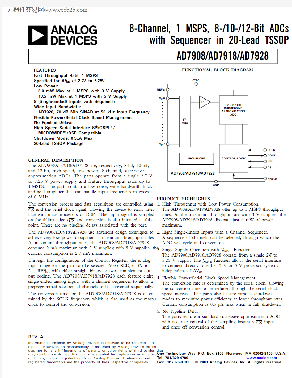
FUNCTIONAL BLOCK DIAGRAM
?
?
?
?
?
?
?
?
?
?
?
?
?
V IN7
SCLK
DOUT
DIN
CS
V DRIVE REF IN
V IN0
FEATURES
Fast Throughput Rate: 1 MSPS
Specified for AV DD of 2.7V to 5.25V
Low Power:
6.0 mW Max at 1 MSPS with 3 V Supply
13.5 mW Max at 1 MSPS with 5 V Supply
8 (Single-Ended) Inputs with Sequencer
Wide Input Bandwidth:
AD7928, 70 dB Min SINAD at 50 kHz Input Frequency Flexible Power/Serial Clock Speed Management
No Pipeline Delays
High Speed Serial Interface SPI?/QSPI?/
MICROWIRE?/DSP Compatible
Shutdown Mode: 0.5 ?A Max
20-Lead TSSOP Package
GENERAL DESCRIPTION
The AD7908/AD7918/AD7928 are, respectively, 8-bit, 10-bit, and 12-bit, high speed, low power, 8-channel, successive approximation ADCs. The parts operate from a single 2.7 V to 5.25 V power supply and feature throughput rates up to 1MSPS. The parts contain a low noise, wide bandwidth track-and-hold amplifier that can handle input frequencies in excess
of 8 MHz.
The conversion process and data acquisition are controlled using CS and the serial clock signal, allowing the device to easily inter-face with microprocessors or DSPs. The input signal is sampled on the falling edge of CS and conversion is also initiated at this point. There are no pipeline delays associated with the part. The AD7908/AD7918/AD7928 use advanced design techniques to achieve very low power dissipation at maximum throughput rates. At maximum throughput rates, the AD7908/AD7918/AD7928 consume 2 mA maximum with 3 V supplies; with 5 V supplies, the current consumption is 2.7 mA maximum.
Through the configuration of the Control Register, the analog input range for the part can be selected as 0V to REF IN or 0V to 2 ? REF IN, with either straight binary or twos complement out-put coding. The AD7908/AD7918/AD7928 each feature eight single-ended analog inputs with a channel sequencer to allow a preprogrammed selection of channels to be converted sequentially. The conversion time for the AD7908/AD7918/AD7928 is deter-mined by the SCLK frequency, which is also used as the master clock to control the conversion.PRODUCT HIGHLIGHTS
1.High Throughput with Low Power Consumption.
The AD7908/AD7918/AD7928 offer up to 1 MSPS throughput rates. At the maximum throughput rate with 3 V supplies, the AD7908/AD7918/AD7928 dissipate just 6 mW of power
maximum.
2.Eight Single-Ended Inputs with a Channel Sequencer.
A sequence of channels can be selected, through which the
ADC will cycle and convert on.
3.Single-Supply Operation with V DRIVE Function.
The AD7908/AD7918/AD7928 operate from a single 2.7V to
5.25 V supply. The V DRIVE function allows the serial interface
to connect directly to either 3 V or 5 V processor systems
independent of AV DD.
4.Flexible Power/Serial Clock Speed Management.
The conversion rate is determined by the serial clock, allowing the conversion time to be reduced through the serial clock
speed increase. The parts also feature various shutdown
modes to maximize power efficiency at lower throughput rates.
Current consumption is 0.5 μA max when in full shutdown.
5. No Pipeline Delay.
The parts feature a standard successive approximation ADC with accurate control of the sampling instant via a CS input and once off conversion control.
AD7908/AD7918/AD7928
REV. A
Parameter
B Version 1
Unit Test Conditions/Comments
DYNAMIC PERFORMANCE
f IN = 50 kHz Sine Wave, f SCLK = 20 MHz
Signal-to-(Noise + Distortion) (SINAD)249dB min Signal-to-Noise Ratio (SNR)2
49dB min Total Harmonic Distortion (THD)2–66dB max Peak Harmonic or Spurious Noise (SFDR)2
–64dB max
Intermodulation Distortion (IMD)2fa = 40.1 kHz, fb = 41.5 kHz
Second Order Terms –90dB typ Third Order Terms –90dB typ Aperture Delay 10ns typ Aperture Jitter
50ps typ Channel-to-Channel Isolation 2–85dB typ f IN = 400 kHz Full Power Bandwidth 8.2MHz typ @ 3 dB 1.6
MHz typ @ 0.1 dB
DC ACCURACY 2Resolution
8Bits
Integral Nonlinearity ±0.2LSB max Differential Nonlinearity ±0.2LSB max Guaranteed No Missed Codes to 8 Bits 0 V to REF IN Input Range Straight Binary Output Coding
Offset Error
±0.5LSB max Offset Error Match ±0.05LSB max Gain Error
±0.2LSB max Gain Error Match
±0.05LSB max 0 V to 2 ? REF IN Input Range –REF IN to +REF IN Biased about REF IN with Positive Gain Error
±0.2LSB max Twos Complement Output Coding Positive Gain Error Match ±0.05LSB max Zero Code Error
±0.5LSB max Zero Code Error Match ±0.1LSB max Negative Gain Error
±0.2LSB max Negative Gain Error Match ±0.05LSB max ANALOG INPUT
Input Voltage Ranges 0 to REF IN
V RANGE Bit Set to 1
0 to 2 ? REF IN V
RANGE Bit Set to 0, AV DD /V DRIVE = 4.75 V to 5.25V
DC Leakage Current ±1μA max Input Capacitance 20pF typ REFERENCE INPUT REF IN Input Voltage 2.5V
±1% Specified Performance DC Leakage Current ±1μA max REF IN Input Impedance 36
k ? typ f SAMPLE = 1 MSPS
LOGIC INPUTS
Input High Voltage, V INH 0.7 ? V DRIVE V min Input Low Voltage, V INL 0.3 ? V DRIVE V max Input Current, I IN
±1μA max Typically 10 nA, V IN = 0 V or V DRIVE
Input Capacitance, C IN 3
10
pF max
LOGIC OUTPUTS
Output High Voltage, V OH V DRIVE – 0.2V min I SOURCE = 200 μA, AV DD = 2.7 V to 5.25 V Output Low Voltage, V OL
0.4V max I SINK = 200 μA Floating-State Leakage Current ±1μA max Floating-State Output Capacitance 310pF max Output Coding
Straight (Natural) Binary Coding Bit Set to 1Twos Complement Coding Bit Set to 0
CONVERSION RATE Conversion Time
800ns max 16 SCLK Cycles with SCLK at 20 MHz Track-and-Hold Acquisition Time 300ns max Sine Wave Input 300ns max Full-Scale Step Input
Throughput Rate
1
MSPS max See Serial Interface Section
(AV DD = V DRIVE = 2.7V to 5.25V, REF IN = 2.5V, f SCLK = 20MHz, T A = T MIN to T MAX , unless otherwise noted.)
AD7908–SPECIFICATIONS
–2–
AD7908/AD7918/AD7928
REV. A Parameter
B Version 1Unit Test Conditions/Comments
POWER REQUIREMENTS AV DD 2.7/5.25V min/max V DRIVE 2.7/5.25V min/max I DD 4
Digital I/Ps = 0 V or V DRIVE
Normal Mode (Static)
600μA typ AV DD = 2.7 V to 5.25 V, SCLK On or Off Normal Mode (Operational)
2.7mA max AV DD = 4.75 V to 5.25 V, f SCLK = 20 MHz 2mA max AV DD = 2.7 V to
3.6 V, f SCLK = 20 MHz Using Auto Shutdown Mode 960μA typ f SAMPLE = 250 kSPS 0.5μA max (Static)
Full Shutdown Mode 0.5μA max SCLK On or Off (20 nA typ)Power Dissipation 4
Normal Mode (Operational)13.5mW max AV DD = 5 V, f SCLK = 20 MHz 6mW max AV DD = 3 V, f SCLK = 20 MHz Auto Shutdown Mode (Static) 2.5μW max AV DD = 5 V 1.5μW max AV DD = 3 V Full Shutdown Mode
2.5μW max AV DD = 5 V 1.5
μW max
AV DD = 3 V
NOTES 1
Temperature ranges as follows: B Version: –40°C to +85°C.2
See Terminology section.3
Sample tested @ 25°C to ensure compliance.4
See Power vs. Throughput Rate section.
Specifications subject to change without notice.
–3–
AD7908/AD7918/AD7928
REV. A
Parameter
B Version 1Unit Test Conditions/Comments
DYNAMIC PERFORMANCE
f IN = 50 kHz Sine Wave, f SCLK = 20 MHz
Signal-to-(Noise + Distortion) (SINAD)261dB min Signal-to-Noise Ratio (SNR)2
61dB min Total Harmonic Distortion (THD)2–72dB max Peak Harmonic or Spurious Noise (SFDR)2
–74dB max
Intermodulation Distortion (IMD)2fa = 40.1 kHz, fb = 41.5 kHz
Second Order Terms –90dB typ Third Order Terms –90dB typ Aperture Delay 10ns typ Aperture Jitter
50ps typ Channel-to-Channel Isolation 2–85dB typ f IN = 400 kHz Full Power Bandwidth 8.2MHz typ @ 3 dB 1.6MHz typ @ 0.1 dB
DC ACCURACY 2Resolution
10Bits
Integral Nonlinearity ±0.5LSB max Differential Nonlinearity ±0.5LSB max Guaranteed No Missed Codes to 10 Bits 0 V to REF IN Input Range Straight Binary Output Coding
Offset Error
±2LSB max Offset Error Match ±0.2LSB max Gain Error
±0.5LSB max Gain Error Match
±0.2LSB max 0 V to 2 ? REF IN Input Range –REF IN to +REF IN Biased about REF IN with Positive Gain Error
±0.5LSB max Twos Complement Output Coding Positive Gain Error Match ±0.2LSB max Zero Code Error
±2LSB max Zero Code Error Match ±0.2LSB max Negative Gain Error
±0.5LSB max Negative Gain Error Match ±0.2
LSB max ANALOG INPUT
Input Voltage Ranges 0 to REF IN
V RANGE Bit Set to 1
0 to 2 ? REF IN V
RANGE Bit Set to 0, AV DD /V DRIVE = 4.75 V to 5.25V
DC Leakage Current ±1μA max Input Capacitance 20pF typ REFERENCE INPUT REF IN Input Voltage 2.5V
±1% Specified Performance DC Leakage Current ±1μA max REF IN Input Impedance 36
k ? typ f SAMPLE = 1 MSPS
LOGIC INPUTS
Input High Voltage, V INH 0.7 ? V DRIVE V min Input Low Voltage, V INL 0.3 ? V DRIVE V max Input Current, I IN
±1μA max Typically 10 nA, V IN = 0 V or V DRIVE
Input Capacitance, C IN 3
10
pF max
LOGIC OUTPUTS
Output High Voltage, V OH V DRIVE – 0.2V min I SOURCE = 200 μA, AV DD = 2.7 V to 5.25 V Output Low Voltage, V OL
0.4V max I SINK = 200 μA Floating-State Leakage Current ±1μA max Floating-State Output Capacitance 310pF max Output Coding
Straight (Natural) Binary Coding Bit Set to 1Twos Complement Coding Bit Set to 0
CONVERSION RATE Conversion Time
800ns max 16 SCLK Cycles with SCLK at 20 MHz Track-and-Hold Acquisition Time 300ns max Sine Wave Input 300ns max Full-Scale Step Input
Throughput Rate
1
MSPS max
See Serial Interface Section
(AV DD = V DRIVE = 2.7V to 5.25V, REF IN = 2.5V, f SCLK = 20MHz, T A = T MIN to T MAX , unless otherwise noted.)
AD7918–SPECIFICATIONS
–4–
AD7908/AD7918/AD7928
REV. A Parameter
B Version 1Unit Test Conditions/Comments
POWER REQUIREMENTS AV DD 2.7/5.25V min/max V DRIVE 2.7/5.25V min/max I DD 4
Digital I/Ps = 0 V or V DRIVE
Normal Mode (Static)
600μA typ AV DD = 2.7 V to 5.25 V, SCLK On or Off Normal Mode (Operational)
2.7mA max AV DD = 4.75 V to 5.25 V, f SCLK = 20 MHz 2mA max AV DD = 2.7 V to
3.6 V, f SCLK = 20 MHz Using Auto Shutdown Mode 960μA typ f SAMPLE = 250 kSPS 0.5μA max (Static)
Full Shutdown Mode 0.5μA max SCLK On or Off (20 nA typ)Power Dissipation 4
Normal Mode (Operational)13.5mW max AV DD = 5 V, f SCLK = 20 MHz 6mW max AV DD = 3 V, f SCLK = 20 MHz Auto Shutdown Mode (Static) 2.5μW max AV DD = 5 V 1.5μW max AV DD = 3 V Full Shutdown Mode
2.5μW max AV DD = 5 V 1.5
μW max
AV DD = 3 V
NOTES 1
Temperature ranges as follows: B Version: –40°C to +85°C.2
See Terminology section.3
Sample tested @ 25°C to ensure compliance.4
See Power vs. Throughput Rate section.
Specifications subject to change without notice.
–5–
AD7908/AD7918/AD7928
REV. A
(AV DD = V DRIVE = 2.7V to 5.25V, REF IN = 2.5V, f SCLK = 20MHz, T A = T MIN to T MAX , unless otherwise noted.)
Parameter
B Version 2
Unit Test Conditions/Comments
DYNAMIC PERFORMANCE
f IN = 50 kHz Sine Wave, f SCLK = 20 MHz Signal-to-(Noise + Distortion) (SINAD)270dB min @ 5 V
69dB min @ 3 V Typically 70 dB Signal-to-Noise Ratio (SNR)2
70dB min Total Harmonic Distortion (THD)2–77dB max @ 5 V Typically –84 dB –73dB max @ 3 V Typically –77 dB Peak Harmonic or Spurious Noise –78dB max @ 5 V Typically –86 dB (SFDR)2
–76dB max @ 3 V Typically –80 dB
Intermodulation Distortion (IMD)2fa = 40.1 kHz, fb = 41.5 kHz
Second Order Terms –90dB typ Third Order Terms –90dB typ Aperture Delay 10ns typ Aperture Jitter
50ps typ Channel-to-Channel Isolation 2–85dB typ f IN = 400 kHz Full Power Bandwidth 8.2MHz typ @ 3 dB 1.6
MHz typ @ 0.1 dB
DC ACCURACY 2Resolution
12Bits
Integral Nonlinearity ±1
LSB max Differential Nonlinearity –0.9/+1.5LSB max Guaranteed No Missed Codes to 12 Bits 0 V to REF IN Input Range Straight Binary Output Coding Offset Error
±8LSB max Typically ±0.5 LSB
Offset Error Match ±0.5LSB max Gain Error
±1.5LSB max Gain Error Match
±0.5LSB max 0 V to 2 ? REF IN Input Range –REF IN to +REF IN Biased about REF IN with Positive Gain Error
±1.5LSB max Twos Complement Output Coding Positive Gain Error Match ±0.5LSB max Zero Code Error
±8LSB max Typically ±0.8 LSB
Zero Code Error Match ±0.5LSB max Negative Gain Error
±1LSB max Negative Gain Error Match ±0.5
LSB max ANALOG INPUT
Input Voltage Ranges 0 to REF IN
V RANGE Bit Set to 1
0 to 2 ? REF IN V
RANGE Bit Set to 0, AV DD /V DRIVE = 4.75 V to 5.25V
DC Leakage Current ±1μA max Input Capacitance 20pF typ REFERENCE INPUT REF IN Input Voltage 2.5V
±1% Specified Performance DC Leakage Current ±1μA max REF IN Input Impedance 36
k ? typ f SAMPLE = 1 MSPS
LOGIC INPUTS
Input High Voltage, V INH 0.7 ? V DRIVE V min Input Low Voltage, V INL 0.3 ? V DRIVE V max Input Current, I IN
±1μA max Typically 10 nA, V IN = 0 V or V DRIVE
Input Capacitance, C IN 3
10
pF max
LOGIC OUTPUTS
Output High Voltage, V OH V DRIVE – 0.2V min I SOURCE = 200 μA, AV DD = 2.7 V to 5.25 V Output Low Voltage, V OL
0.4V max I SINK = 200 μA Floating-State Leakage Current ±1μA max Floating-State Output Capacitance 310pF max Output Coding
Straight (Natural) Binary Coding Bit Set to 1Twos Complement
Coding Bit Set to 0
AD7928–SPECIFICATIONS
–6–
AD7908/AD7918/AD7928
REV. A Parameter
B Version 1Unit Test Conditions/Comments
CONVERSION RATE Conversion Time
800ns max 16 SCLK Cycles with SCLK at 20 MHz Track-and-Hold Acquisition Time 300ns max Sine Wave Input 300ns max Full-Scale Step Input
Throughput Rate
1MSPS max See Serial Interface Section
POWER REQUIREMENTS AV DD 2.7/5.25V min/max V DRIVE 2.7/5.25V min/max I DD 4
Digital I/Ps = 0 V or V DRIVE
Normal Mode (Static)
600μA typ AV DD = 2.7 V to 5.25 V, SCLK On or Off Normal Mode (Operational)
2.7mA max AV DD = 4.75 V to 5.25 V, f SCLK = 20 MHz 2mA max AV DD = 2.7 V to
3.6 V, f SCLK = 20 MHz Using Auto Shutdown Mode 960μA typ f SAMPLE = 250 kSPS 0.5μA max (Static)
Full Shutdown Mode 0.5μA max SCLK On or Off (20 nA typ)Power Dissipation 4
Normal Mode (Operational)13.5mW max AV DD = 5 V, f SCLK = 20 MHz 6mW max AV DD = 3 V, f SCLK = 20 MHz Auto Shutdown Mode (Static) 2.5μW max AV DD = 5 V 1.5μW max AV DD = 3 V Full Shutdown Mode
2.5μW max AV DD = 5 V 1.5
μW max
AV DD = 3 V
NOTES 1
Temperature ranges as follows: B Version: –40°C to +85°C.2
See Terminology section.3
Sample tested @ 25°C to ensure compliance.4
See Power vs. Throughput Rate section.
Specifications subject to change without notice.
–7–
AD7908/AD7918/AD7928REV. A
TIMING SPECIFICATIONS 1
(AV DD = 2.7 V to 5.25 V, V DRIVE < AV DD , REF IN = 2.5 V, T A = T MIN to T MAX , unless otherwise noted.)
Limit at T MIN , T MAX AD7908/AD7918/AD7928Parameter AV DD = 3 V AV DD = 5 V Unit
Description
f SCLK 21010
kHz min 20
20
MHz max t CONVERT 16 ? t SCLK 16 ? t SCLK t QUIET 5050ns min Minimum Quiet Time Required between CS Rising Edge and Start of Next Conversion t 21010ns min CS to SCLK Setup Time
t 333530ns max
Delay from CS until DOUT Three-State Disabled t 4340
40
ns max Data Access Time after SCLK Falling Edge t 50.4 ? t SCLK 0.4 ? t SCLK ns min SCLK Low Pulse Width t 60.4 ? t SCLK 0.4 ? t SCLK ns min SCLK High Pulse Width
t 71010ns min SCLK to DOUT Valid Hold Time
t 8415/4515/35ns min/max SCLK Falling Edge to DOUT High Impedance t 91010ns min DIN Setup Time Prior to SCLK Falling Edge t 1055ns min DIN Hold Time after SCLK Falling Edge t 112020ns min Sixteenth SCLK Falling Edge to CS High
t 12
1
1
μs max
Power-Up Time from Full Power-Down/Auto Shutdown Mode
NOTES 1
Sample tested at 25°C to ensure compliance. All input signals are specified with tr = tf = 5 ns (10% to 90% of AV DD ) and timed from a voltage level of 1.6 V.See Figure 1. The 3 V operating range spans from 2.7 V to 3.6 V. The 5 V operating range spans from 4.75 V to 5.25 V.2
Mark/Space ratio for the SCLK input is 40/60 to 60/40.3
Measured with the load circuit of Figure 1 and defined as the time required for the output to cross 0.4 V or 0.7 ? V DRIVE .4
t 8 is derived from the measured time taken by the data outputs to change 0.5 V when loaded with the circuit of Figure 1. The measured number is then extrapolated back to remove the effects of charging or discharging the 50 pF capacitor. This means that the time ,t 8, quoted in the timing characteristics is the true bus relinquish time of the part and is independent of the bus loading.Specifications subject to change without notice.
TO OUTPUT
PIN
Figure 1.Load Circuit for Digital Output Timing Specifications
–8–
AD7908/AD7918/AD7928
REV. A ABSOLUTE MAXIMUM RATINGS 1
(T A = 25°C, unless otherwise noted.)
AV DD to AGND . . . . . . . . . . . . . . . . . . . . . . . –0.3 V to +7 V V DRIVE to AGND . . . . . . . . . . . . . . . . –0.3 V to AV DD + 0.3 V Analog Input Voltage to AGND . . . . –0.3 V to AV DD + 0.3 V Digital Input Voltage to AGND . . . . . . . . . . . . –0.3 V to +7 V Digital Output Voltage to AGND . . . –0.3 V to AV DD + 0.3 V REF IN to AGND . . . . . . . . . . . . . . . . –0.3 V to AV DD + 0.3 V Input Current to Any Pin Except Supplies 2 . . . . . . . . ±10 mA Operating Temperature Range
Commercial (B Version) . . . . . . . . . . . . . . –40°C to +85°C Storage Temperature Range . . . . . . . . . . . –65°C to +150°C Junction Temperature . . . . . . . . . . . . . . . . . . . . . . . . . . 150°C
TSSOP Package, Power Dissipation . . . . . . . . . . . . . 450 mW q JA Thermal Impedance . . . . . . . . . . . . . 143°C/W (TSSOP)q JC Thermal Impedance . . . . . . . . . . . . . . 45°C/W (TSSOP)Lead Temperature, Soldering
Vapor Phase (60 sec) . . . . . . . . . . . . . . . . . . . . . . . . . 215°C Infrared (15 sec) . . . . . . . . . . . . . . . . . . . . . . . . . . . . 220°C ESD . . . . . . . . . . . . . . . . . . . . . . . . . . . . . . . . . . . . . . . . . .2 kV
NOTES 1
Stresses above those listed under Absolute Maximum Ratings may cause perma-nent damage to the device. This is a stress rating only and functional operation of the device at these or any other conditions above those listed in the operational sections of this specification is not implied. Exposure to absolute maximum rating conditions for extended periods may affect device reliability.2
Transient currents of up to 100 mA will not cause SCR latch-up.
–9–
CAUTION
ESD (electrostatic discharge) sensitive device. Electrostatic charges as high as 4000V readily accumulate on the human body and test equipment and can discharge without detection. Although the AD7908/AD7918/AD7928 feature proprietary ESD protection circuitry, permanent damage may occur on devices subjected to high energy electrostatic discharges. Therefore, proper ESD precautions
are recommended to avoid performance degradation or loss of functionality.
ORDERING GUIDE
Temperature Linearity Package Package Model
Range Error (LSB)1Option Description AD7908BRU
–40°C to +85°C ?0.2RU-20TSSOP AD7908BRU-REEL –40°C to +85°C ?0.2RU-20TSSOP AD7908BRU-REEL7–40°C to +85°C ?0.2RU-20TSSOP AD7918BRU
–40°C to +85°C ?0.5RU-20TSSOP AD7918BRU-REEL –40°C to +85°C ?0.5RU-20TSSOP AD7918BRU-REEL7–40°C to +85°C ?0.5RU-20TSSOP AD7928BRU
–40°C to +85°C ?1RU-20TSSOP AD7928BRU-REEL –40°C to +85°C ?1RU-20TSSOP AD7928BRU-REEL7–40°C to +85°C
?1
RU-20
TSSOP
EVAL-AD79x8CB 2
Evaluation Board EVAL-CONTROL BRD 3
Controller Board
NOTES 1
Linearity error here refers to integral linearity error.2
This can be used as a standalone evaluation board or in conjunction with the Evaluation Controller Board for evaluation/demonstration purposes.The board comes with one chip of each the AD7908, AD7918, and AD7928.3
This board is a complete unit allowing a PC to control and communicate with all Analog Devices evaluation boards ending in the CB designators.To order a complete evaluation kit, order the particular ADC evaluation board, e.g., EVAL-AD79x8CB, the EVAL-CONTROL BRD2,and a 12 V ac transformer. See relevant Evaluation Board Technical Note for more information.
AD7908/AD7918/AD7928
REV. A
PIN FUNCTION DESCRIPTIONS
Pin No.Mnemonic Function
1SCLK Serial Clock. Logic input. SCLK provides the serial clock for accessing data from the part. This clock
input is also used as the clock source for the AD7908/AD7918/AD7928’s conversion process.
2DIN Data In. Logic input. Data to be written to the AD7908/AD7918/AD7928’s Control Register is provided on this input and is clocked into the register on the falling edge of SCLK (see the Control Register section).3
CS Chip Select. Active low logic input. This input provides the dual function of initiating conversions on the AD7908/AD7918/AD7928, and also frames the serial data transfer.
4, 8, 17, 20
AGND
Analog Ground. Ground reference point for all analog circuitry on the AD7908/AD7918/AD7928.All analog input signals and any external reference signal should be referred to this AGND voltage.All AGND pins should be connected together.
5, 6AV DD Analog Power Supply Input. The AV DD range for the AD7908/AD7918/AD7928 is from 2.7 V to 5.25 V.For the 0 V to 2 ? REF IN range, AV DD should be from 4.75 V to 5.25 V.
7REF IN Reference Input for the AD7908/AD7918/AD7928. An external reference must be applied to this input.The voltage range for the external reference is 2.5 V ± 1% for specified performance.
16–9
V IN 0–V IN 7
Analog Input 0 through Analog Input 7. Eight single-ended analog input channels that are multiplexed into the on-chip track-and-hold. The analog input channel to be converted is selected by using the address bits ADD2 through ADD0 of the Control Register. The address bits, in conjunction with the SEQ and SHADOW bits, allow the Sequencer to be programmed. The input range for all input channels can extend from 0 V to REF IN or 0 V to 2 ? REF IN as selected via the RANGE bit in the Control Register. Any unused input channels must be connected to AGND to avoid noise pickup.
18DOUT
Data Out. Logic output. The conversion result from the AD7908/AD7918/AD7928 is provided on this output as a serial data stream. The bits are clocked out on the falling edge of the SCLK input. The data stream from the AD7908 consists of one leading zero, three address bits indicating which channel the conversion result corresponds to, followed by the eight bits of conversion data, followed by four trailing zeros, provided MSB first; the data stream from the AD7918 consists of one leading zero,three address bits indicating which channel the conversion result corresponds to, followed by the 10bits of conversion data, followed by two trailing zeros, also provided MSB first; the data stream from the AD7928 consists of one leading zero, three address bits indicating which channel the conversion result corresponds to, followed by the 12 bits of conversion data, provided MSB first. The output coding may be selected as straight binary or twos complement via the CODING bit in the Control Register.19V DRIVE
Logic Power Supply Input. The voltage supplied at this pin determines at what voltage the serial interface of the AD7908/AD7918/AD7928 will operate.
PIN CONFIGURATION
20-Lead TSSOP
AGND V DRIVE DOUT AGND AV V IN 0
AV V IN
1
REF V IN 2V IN 3V IN V IN 4V IN V IN 5
–10–
AD7908/AD7918/AD7928
REV. A TERMINOLOGY Integral Nonlinearity
This is the maximum deviation from a straight line passing through the endpoints of the ADC transfer function. The end-points of the transfer function are zero scale, a point 1 LSB below the first code transition, and full scale, a point 1 LSB above the last code transition.
Differential Nonlinearity
This is the difference between the measured and the ideal 1 LSB change between any two adjacent codes in the ADC.
Offset Error
This is the deviation of the first code transition (00 . . . 000) to (00 . . . 001) from the ideal, i.e., AGND + 1 LSB.
Offset Error Match
This is the difference in offset error between any two channels.
Gain Error
This is the deviation of the last code transition (111 . . . 110) to (111 . . . 111) from the ideal (i.e., REF IN – 1 LSB) after the offset error has been adjusted out.
Gain Error Match
This is the difference in Gain Error between any two channels.
Zero Code Error
This applies when using the twos complement output coding option, in particular to the 2 ? REF IN input range with –REF IN to +REF IN biased about the REF IN point. It is the deviation of the midscale transition (all 0s to all 1s) from the ideal V IN voltage,i.e., REF IN – 1 LSB.
Zero Code Error Match
This is the difference in Zero Code Error between any two channels.
Positive Gain Error
This applies when using the twos complement output coding option, in particular to the 2 ? REF IN input range with –REF IN to +REF IN biased about the REF IN point. It is the deviation of the last code transition (011. . .110) to (011 . . . 111) from the ideal (i.e., +REF IN – 1 LSB) after the Zero Code Error has been adjusted out.
Positive Gain Error Match
This is the difference in Positive Gain Error between any two
channels.
Negative Gain Error
This applies when using the twos complement output coding option, in particular to the 2 ? REF IN input range with –REF IN to +REF IN biased about the REF IN point. It is the deviation of the first code transition (100 . . . 000) to (100 . . . 001) from the ideal (i.e., –REF IN + 1 LSB) after the Zero Code Error has been adjusted out.
Negative Gain Error Match
This is the difference in Negative Gain Error between any two channels.
Channel-to-Channel Isolation
Channel-to-channel isolation is a measure of the level of crosstalk between channels. It is measured by applying a full-scale 400 kHz sine wave signal to all seven nonselected input channels and deter-mining how much that signal is attenuated in the selected channel with a 50 kHz signal. The figure is given worst case across all eight channels for the AD7908/AD7918/AD7928.
PSR (Power Supply Rejection)
Variations in power supply will affect the full scale transition, but not the converter ’s linearity. Power supply rejection is the maxi-mum change in full-scale transition point due to a change in power-supply voltage from the nominal value. See Typical Performance Curves.
Track-and-Hold Acquisition Time
The track-and-hold amplifier returns into track mode at the end of conversion. Track-and-hold acquisition time is the time required for the output of the track-and-hold amplifier to reach its final value, within ±1 LSB, after the end of conversion.
Signal-to-(Noise + Distortion) Ratio
This is the measured ratio of signal-to-(noise + distortion) at the output of the A/D converter. The signal is the rms amplitude of the fundamental.Noise is the sum of all nonfundamental signals up to half the sampling frequency (f S /2), excluding dc. The ratio is dependent on the number of quantization levels in the digiti-zation process; the more levels, the smaller the quantization noise. The theoretical signal-to-(noise + distortion) ratio for an ideal N-bit converter with a sine wave input is given by:
Signal to Noise Distortion N dB --()(..)+=+602176Thus for a 12-bit converter, this is 74dB; for a 10-bit converter,this is 62 dB; and for an 8-bit converter, this is 50 dB.
Total Harmonic Distortion
Total harmonic distortion (THD) is the ratio of the rms sum of harmonics to the fundamental. For the AD7908/AD7918/AD7928, it is defined as:
THD dB V V V V V V ()log
=++++202232425262
1
where V 1 is the rms amplitude of the fundamental and V 2, V 3,V 4, V 5, and V 6 are the rms amplitudes of the second through the sixth harmonics.
–11–
AD7908/AD7918/AD7928–Typical Performance Characteristics
REV. A
PERFORMANCE CURVES
TPC 1 shows a typical FFT plot for the AD7928 at 1 MSPS sample rate and 50 kHz input frequency. TPC 2 shows the signal-to-(noise + distortion) ratio performance versus input frequency for various supply voltages while sampling at 1 MSPS with an SCLK of 20 MHz.
TPC 3 shows the power supply rejection ratio versus supply ripple frequency for the AD7928 when no decoupling is used.The power supply rejection ratio is defined as the ratio of the power in the ADC output at full-scale frequency f, to the power of a 200 mV p-p sine wave applied to the ADC AV DD supply of frequency f S :
PSRR dB Pf Pfs ()log(/)=10Pf is equal to the power at frequency f in ADC output; Pf S is
equal to the power at frequency f S coupled onto the ADC AV DD supply. Here a 200 mV p-p sine wave is coupled onto the AV DD supply.
TPC 4 shows a graph of total harmonic distortion versus analog input frequency for various supply voltages, while TPC 5 shows a graph of total harmonic distortion versus analog input frequency for various source impedances. See the Analog Input section.TPC 6 and TPC 7 show typical INL and DNL plots for the AD7928.
FREQUENCY (kHz)
0100200300400500
S N R (d B )
50150
2503504504096 POINT FFT AV DD = 5V
f SAMPLE = 1MSPS f IN = 50kHz
SINAD = 71.147dB THD = –87.229dB SFDR = –90.744dB
TPC 1.AD7928 Dynamic Performance at 1 MSPS
INPUT FREQUENCY (kHz)
75
10
1000
S I N A D (d B )
70
65
60
55100
TPC 2.AD7928 SINAD vs. Analog Input Frequency for Various Supply Voltages at 1 MSPS
SUPPL Y RIPPLE FREQUENCY (kHz)
1000
P S R R (d B )
–40–60–80–90
500–20–50–70900
800
700600400300200100
–10–30
TPC 3.AD7928 PSRR vs. Supply Ripple Frequency
INPUT FREQUENCY (kHz)
–50
10
1000
T H D (d B )
–65
–75–85
–90
–60
–70–80
100
–55
TPC 4.AD7928 THD vs. Analog Input Frequency for Various Supply Voltages at 1 MSPS
INPUT FREQUENCY (kHz)
–50
10
1000
T H D
(d B )
–65
–75–85–90
–60
–70
–80100
–55TPC 5.AD7928 THD vs. Analog Input Frequency for Various Source Impedances
–12–
AD7908/AD7918/AD7928
REV. A
Table I.Control Register Bit Functions
MSB LSB
WRITE SEQ
DONTC ADD2ADD1ADD0PM1
PM0
SHADOW
DONTC
RANGE
CODING
Bit Mnemonic Comment
11
WRITE
The value written to this bit of the Control Register determines whether or not the following 11 bits will be loaded to the Control Register. If this bit is a 1, the following 11 bits will be written to the Control Register; if it is a 0, the remaining 11 bits are not loaded to the Control Register, and it remains unchanged.
10SEQ The SEQ bit in the Control Register is used in conjunction with the SHADOW bit to control the use of the sequencer function and access the SHADOW Register. (See Table IV.)
9DONTCARE
8–6
ADD2–ADD0These three address bits are loaded at the end of the present conversion sequence and select which analog
input channel is to be converted in the next serial transfer, or they may select the final channel in a consecutive sequence as described in Table IV. The selected input channel is decoded as shown in Table II. The address bits corresponding to the conversion result are also output on DOUT prior to the 12 bits of data,see the Serial Interface section. The next channel to be converted on will be selected by the mux on the 14th SCLK falling edge.5, 4PM1, PM0Power Management Bits. These two bits decode the mode of operation of the AD7908/AD7918/AD7928as shown in Table III.
3SHADOW The SHADOW bit in the Control Register is used in conjunction with the SEQ bit to control the use of the sequencer function and access the SHADOW Register. (See Table IV.)
2DONTCARE 1
RANGE
This bit selects the analog input range to be used on the AD7908/AD7918/AD7928. If it is set to 0, the analog input range will extend from 0 V to 2 ? REF IN . If it is set to 1, the analog input range will extend from 0 V to REF IN (for the next conversion). For 0 V to 2 ? REF IN , AV DD = 4.75 V to 5.25 V.
0CODING
This bit selects the type of output coding the AD7908/AD7918/AD7928 will use for the conversion result.If this bit is set to 0, the output coding for the part will be twos complement. If this bit is set to 1, the output coding from the part will be straight binary (for the next conversion).
CONTROL REGISTER
The Control Register on the AD7908/AD7918/AD7928 is a 12-bit, write-only register. Data is loaded from the DIN pin of the AD7908/AD7918/AD7928 on the falling edge of SCLK. The data is transferred on the DIN line at the same time that the conver-sion result is read from the part. The data transferred on the DIN line corresponds to the AD7908/AD7918/AD7928 configuration for the next conversion. This requires 16 serial clocks for every data transfer. Only the information provided on the first 12 falling clock edges (after CS falling edge) is loaded to the Control Register. MSB denotes the first bit in the data stream. The bit functions are outlined in Table I.
CODE
1.00
4096
I N L E R R O R (L S B )
–0.4–0.8–1.0
0.2–0.2–0.620480.6
AV DD = V DRIVE = 5V TEMP = 25?C
0.4
0.825603072
3584
512
1024
1536
TPC 6.AD7928 Typical INL CODE
1.0
04096
D N L
E R R O R (L S B )
–0.4–0.8
–1.0
0.2–0.2–0.620480.60.40.825603072358451210241536
TPC 7.AD7928 Typical DNL
–13–
AD7908/AD7918/AD7928
REV. A
Table II.Channel Selection
ADD2ADD1ADD0Analog Input Channel 000V IN 0001V IN 1010V IN 2011V IN 3100V IN 4101V IN 5110V IN 61
1
1
V IN 7
Table III.Power Mode Selection
PM1PM0Mode 1
1
Normal Operation . In this mode, the AD7908/AD7918/AD7928 remain in full power mode regardless of the status of any of the logic inputs.This mode allows the fastest possible throughput rate from the AD7908/AD7918/AD7928.10
Full Shutdown . In this mode, the AD7908/AD7918/AD7928 is in full shutdown mode with all circuitry powering down. The AD7908/AD7918/AD7928 retains the information in the Control Register while in full shutdown. The part remains in full shutdown until these bits are changed.01
Auto Shutdown . In this mode, the AD7908/AD7918/AD7928 automatically enters full shutdown mode at the end of each conversion when the control register is updated. Wake-up time from full shutdown is 1 μs and the user should ensure that 1 μs has elapsed before
attempting to perform a valid conversion on the part in this mode.
00
Invalid Selection . This configuration is not allowed.
SEQUENCER OPERATION
The configuration of the SEQ and SHADOW bits in the Control Register allows the user to select a particular mode of operation of the sequencer function. Table IV outlines the four modes of operation of the Sequencer.
Table IV.Sequence Selection
SEQ SHADOW Sequence Type 0
This configuration means that the sequence function is not used. The analog input channel selected for each individual conversion is determined by the contents of the channel address bits ADD0 through ADD2 in each prior write operation. This mode of operation reflects the traditional operation of a multichannel ADC, without the Sequencer function being used, where each write to the AD7908/AD7918/AD7928 selects the next channel for conversion. (See Figure 2.)
1
This configuration selects the SHADOW Register for programming. The following write operation will load the contents of the SHADOW Register. This will program the sequence of channels to be converted on continuously with each successive valid CS falling edge. (See SHADOW Register section, Table V, and Figure 3.) The channels selected need not be consecutive.10
If the SEQ and SHADOW bits are set in this way, then the sequence function will not be interrupted upon completion of the WRITE operation. This allows other bits in the Control Register to be altered between conversions while in a sequence, without terminating the cycle.
1
1This configuration is used in conjunction with the channel address bits ADD2 to ADD0 to program continuous conversions on a consecutive sequence of channels from Channel 0 to a selected final channel as determined by the channel address bits in the Control Register. (See Figure 4.)
–14–
AD7908/AD7918/AD7928
REV. A Table V.SHADOW Register Bit Functions
MSB LSB V IN 0
V IN 1V IN 2
V IN 3
V IN 4
V IN 5
V IN 6
V IN 7
V IN 0
V IN 1
V IN 2
V IN 3
V IN 4
V IN 5
V IN 6
V IN 7
------------------SEQUENCE ONE-------------------------------------------------------SEQUENCE TWO-----------------------
CS
CS
Figure 2.SEQ Bit = 0, SHADOW Bit = 0 Flowchart
SHADOW REGISTER
The SHADOW Register on the AD7908/AD7918/AD7928 is a 16-bit, write-only register. Data is loaded from the DIN pin of the AD7908/AD7918/AD7928 on the falling edge of SCLK.The data is transferred on the DIN line at the same time that a conversion result is read from the part. This requires 16 serial clock falling edges for the data transfer. The information is clocked into the SHADOW Register, provided that the SEQ and SHADOW bits were set to 0,1, respectively, in the previous write to the Control Register. MSB denotes the first bit in the data stream. Each bit represents an analog input from Channel 0 to Channel 7. Through programming the SHADOW Register,two sequences of channels may be selected, through which the AD7908/AD7918/AD7928 will cycle with each consecutive conversion after the write to the SHADOW Register. Sequence One will be performed first and then Sequence Two. If the user
does not wish to perform a second sequence option, then all 0s must be written to the last 8 LSBs of the SHADOW Register.To select a sequence of channels, the associated channel bit must be set for each analog input. The AD7908/AD7918/AD7928 will continuously cycle through the selected channels
in ascending order beginning with the lowest channel, until a write operation occurs (i.e., the WRITE bit is set to 1) with the SEQ and SHADOW bits configured in any way except 1,0.(See Table IV.) The bit functions are outlined in Table V.Figure 2 reflects the traditional operation of a multichannel ADC, where each serial transfer selects the next channel for conversion. In this mode of operation the Sequencer function is not used.
Figure 3 shows how to program the AD7908/AD7918/AD7928to continuously convert on a particular sequence of channels. To exit this mode of operation and revert back to the traditional mode of operation of a multichannel ADC (as outlined in Figure 2), ensure that the WRITE bit = 1 and the SEQ =SHADOW = 0 on the next serial transfer. Figure 4 shows how a sequence of consecutive channels can be converted on without having to program the SHADOW Register or write to the part on each serial transfer. Again to exit this mode of operation and revert back to the traditional mode of operation of a multichannel ADC (as outlined in Figure 2), ensure the WRITE bit = 1 and the SEQ = SHADOW = 0 on the next serial transfer.
CS
CS
CS
Figure 3.SEQ Bit = 0, SHADOW Bit = 1 Flowchart
–15–
AD7908/AD7918/AD7928
REV. A
CS
CS
CS
Figure 4.SEQ Bit = 1, SHADOW Bit = 1 Flowchart CIRCUIT INFORMATION
The AD7908/AD7918/AD7928 are high speed, 8-channel, 8-bit,10-bit, and 12-bit, single supply, A/D converters, respectively.The parts can be operated from a 2.7 V to 5.25 V supply. When operated from either a 5 V or 3 V supply, the AD7908/AD7918/AD7928 are capable of throughput rates of 1 MSPS when provided with a 20 MHz clock.
The AD7908/AD7918/AD7928 provide the user with an on-chip track-and-hold, A/D converter, and a serial interface housed in a 20-lead TSSOP package. The AD7908/AD7918/AD7928 each have eight single-ended input channels with a channel sequencer,allowing the user to select a channel sequence through which the ADC can cycle with each consecutive CS falling edge. The serial clock input accesses data from the part, controls the transfer of data written to the ADC, and provides the clock source for the successive approximation A/D converter. The analog input range for the AD7908/AD7918/AD7928 is 0 V to REF IN or 0V to 2 ? REF IN , depending on the status of Bit 1 in the Control Register. For the 0 to 2 ? REF IN range, the part must be oper-ated from a 4.75 V to 5.25 V supply.
The AD7908/AD7918/AD7928 provide flexible power management options to allow the user to achieve the best power performance for a given throughput rate. These options are selected by pro-gramming the power management bits, PM1 and PM0, in the Control Register.
CONVERTER OPERATION
The AD7908/AD7918/AD7928 are 8-, 10-, and 12-bit succes-sive approximation analog-to-digital converters based around a capacitive DAC, respectively. The AD7908/AD7918/AD7928can convert analog input signals in the range 0 V to REF IN or 0V to 2 ? REF IN . Figures 5 and 6 show simplified schematics of the ADC. The ADC is comprised of control logic, SAR, and
a capacitive DAC, which are used to add and subtract fixed amounts of charge from the sampling capacitor to bring the comparator back into a balanced condition. Figure 5 shows the ADC during its acquisition phase. SW2 is closed and SW1 is in position A. The comparator is held in a balanced condition and the sampling capacitor acquires the signal on the selected V IN
channel.
V IN V IN Figure 5.ADC Acquisition Phase
When the ADC starts a conversion (see Figure 6), SW2 will open and SW1 will move to position B, causing the comparator to become unbalanced. The Control Logic and the Capacitive DAC are used to add and subtract fixed amounts of charge from the sampling capacitor to bring the comparator back into a balanced condition. When the comparator is rebalanced, the conversion is complete. The Control Logic generates the ADC
output code. Figures 8 and 9 show the ADC transfer functions.
V IN V IN Figure 6.ADC Conversion Phase
Analog Input
Figure 7 shows an equivalent circuit of the analog input structure of the AD7908/AD7918/AD7928. The two diodes D1 and D2provide ESD protection for the analog inputs. Care must be taken to ensure that the analog input signal never exceeds the supply rails by more than 300 mV. This will cause these diodes to become forward biased and start conducting current into the substrate. 10mA is the maximum current these diodes can conduct without causing irreversible damage to the part. The capacitor C1 in Figure 7 is typically about 4 pF and can primarily be attrib-uted to pin capacitance. The resistor R1 is a lumped component made up of the on resistance of the track-and-hold switch and also includes the on resistance of the input multiplexer. The total resistance is typically about 400?. The capacitor C2 is the ADC sampling capacitor and has a capacitance of 30 pF typically.For ac applications, removing high frequency components from the analog input signal is recommended by use of an RC low-pass filter on the relevant analog input pin. In applications where harmonic distortion and signal-to-noise ratio are critical, the analog input should be driven from a low impedance source. Large source impedances will significantly affect the ac performance of the ADC. This may necessitate the use of an input buffer ampli-fier. The choice of the op amp will be a function of the particular application.
–16–
AD7908/AD7918/AD7928
REV. A When no amplifier is used to drive the analog input, the source impedance should be limited to low values. The maximum source impedance will depend on the amount of total harmonic distortion (THD) that can be tolerated. The THD will increase as the source impedance increases, and performance will degrade. (See TPC 5.)
V
Figure 7.Equivalent Analog Input Circuit
ADC TRANSFER FUNCTION
The output coding of the AD7908/AD7918/AD7928 is either straight binary or twos complement, depending on the status of the LSB in the Control Register. The designed code transitions occur at successive LSB values (i.e., 1 LSB, 2LSBs, and so on).The LSB size is REF IN /256 for the AD7908, REF IN /1024 for the AD7918, and REF IN /4096 for the AD7928. The ideal transfer characteristic for the AD7908/AD7918/AD7928 when straight binary coding is selected is shown in Figure 8, and the ideal transfer characteristic for the AD7908/AD7918/AD7928 when twos complement coding is selected is shown in Figure 9.
000 (000)
ANALOG INPUT
111...111000...001000...010111 (110)
??
111 (000)
?
011 (111)
??
NOTE: V REF IS EITHER REF IN OR 2 ? REF IN
Figure 8.Straight Binary Transfer Characteristic
A D C C O D E
ANALOG INPUT
V REF ? 1LSB
100 (000)
011...111100...001100...010011 (110)
??000...001111 (111)
??000…000Figure 9.Twos Complement Transfer Characteristic with REF IN ± REF IN Input Range
Handling Bipolar Input Signals
Figure 10 shows how useful the combination of the 2 ? REF IN input range and the twos complement output coding scheme is for handling bipolar input signals. If the bipolar input signal is biased about REF IN and twos complement output coding is selected, then REF IN becomes the zero code point, –REF IN is negative full scale and +REF IN becomes positive full scale, with a dynamic range of 2 ? REF IN .
TYPICAL CONNECTION DIAGRAM
Figure 11 shows a typical connection diagram for the AD7908/
AD7918/AD7928. In this setup, the AGND pin is connected to the analog ground plane of the system. In Figure 11, REF IN is connected to a decoupled 2.5 V supply from a reference source,the AD780, to provide an analog input range of 0 V to 2.5V (if RANGE bit is 1) or 0 V to 5 V (if RANGE bit is 0). Although the AD7908/AD7918/AD7928 is connected to a V DD of 5 V, the serial interface is connected to a 3 V microprocessor. The V DRIVE pin of the AD7908/AD7918/AD7928 is connected to the same 3V supply of the microprocessor to allow a 3 V logic interface (see the Digital Inputs section). The conversion result is output in a 16-bit word. This 16-bit data stream consists of a leading zero,three address bits indicating which channel the conversion result corresponds to, followed by the 12 bits of conversion data for the AD7928 (10 bits of data for the AD7918 and 8 bits of data for the AD7908, each followed by two and four trailing zeros, respec-tively). For applications where power consumption is of
011 (111)
000 (000)
100 (000)
0V
Figure 10.Handling Bipolar Signals
–17–
AD7908/AD7918/AD7928
REV. A
concern, the power-down modes should be used between
conversions or bursts of several conversions to improve power performance. (See the Modes of Operation section.)
NOTE: ALL UNUSED INPUT CHANNELS SHOULD BE CONNECTED TO AGND
Figure 11.Typical Connection Diagram
Analog Input Selection
Any one of eight analog input channels may be selected for
conversion by programming the multiplexer with the address bits ADD2–ADD0 in the Control Register. The channel configurations are shown in Table II. The AD7908/AD7918/AD7928 may also be configured to automatically cycle through a number of channels as selected. The sequencer feature is accessed via the SEQ and SHADOW bits in the Control Register. (See Table IV.)The AD7908/AD7918/AD7928 can be programmed to continu-ously convert on a selection of channels in ascending order. The analog input channels to be converted on are selected through programming the relevant bits in the SHADOW Register (see Table V). The next serial transfer will then act on the sequence programmed by executing a conversion on the lowest channel in the selection. The next serial transfer will result in a conversion on the next highest channel in the sequence, and so on.It is not necessary to write to the Control Register once a
sequencer operation has been initiated. The WRITE bit must be set to zero or the DIN line tied low to ensure the Control Register is not accidently overwritten, or the sequence operation inter-rupted. If the Control Register is written to at any time during the sequence, then it must be ensured that the SEQ and SHADOW bits are set to 1,0 to avoid interrupting the automatic conversion sequence. This pattern will continue until such time as the AD7908/AD7918/AD7928 is written to and the SEQ and SHADOW bits are configured with any bit combination except 1,0. On completion of the sequence, the AD7908/AD7918/AD7928 sequencer will return to the first selected channel in the SHADOW Register and commence the sequence again.Rather than selecting a particular sequence of channels, a num-ber of consecutive channels beginning with Channel 0 may also be programmed via the Control Register alone, without needing to write to the SHADOW Register. This is possible if the SEQ and SHADOW bits are set to 1,1. The channel address bits ADD2 through ADD0 will then determine the final channel in the consecutive sequence. The next conversion will be on Chan-nel 0, then Channel 1, and so on until the channel selected via the address bits ADD2 through ADD0 is reached. The cycle will begin again on the next serial transfer, provided the WRITE bit is set to low, or if high, that the SEQ and SHADOW bits are set to 1,0; then the ADC will continue its preprogrammed auto-matic sequence uninterrupted.
Regardless of which channel selection method is used, the 16-bit word output from the AD7928 during each conversion will always contain a leading zero, three channel address bits that the conversion result corresponds to, followed by the 12-bit conversion result; the AD7918 will output a leading zero, three channel address bits that the conversion result corresponds to,followed by the 10-bit conversion result and two trailing zeros; the AD7908 will output a leading zero, three channel address bits that the conversion result corresponds to, followed by the 8-bit conver-sion result and four trailing zeros. (See the Serial Interface section.)
Digital Inputs
The digital inputs applied to the AD7908/AD7918/AD7928 are not limited by the maximum ratings that limit the analog inputs.Instead, the digital inputs applied can go to 7 V and are not restricted by the AV DD + 0.3 V limit as on the analog inputs.Another advantage of SCLK, DIN, and CS not being restricted by the AV DD + 0.3 V limit is the fact that power supply sequenc-ing issues are avoided. If CS , DIN, or SCLK are applied before AV DD , there is no risk of latch-up as there would be on the analog inputs if a signal greater than 0.3 V was applied prior to AV DD .
V DRIVE
The AD7908/AD7918/AD7928 also have the V DRIVE feature.V DRIVE controls the voltage at which the serial interface operates.V DRIVE allows the ADC to easily interface to both 3 V and 5V processors. For example, if the AD7908/AD7918/AD7928 were operated with an AV DD of 5 V, the V DRIVE pin could be powered from a 3 V supply. The AD7908/AD7918/AD7928 have better dynamic performance with an AV DD of 5 V while still being able to interface to 3 V processors. Care should be taken to ensure V DRIVE does not exceed AV DD by more than 0.3 V. (See the Absolute Maximum Ratings.)
Reference
An external reference source should be used to supply the 2.5 V reference to the AD7908/AD7918/AD7928. Errors in the refer-ence source will result in gain errors in the AD7908/AD7918/AD7928 transfer function and will add to the specified full-scale errors of the part. A capacitor of at least 0.1 μF should be placed on the REF IN pin. Suitable reference sources for the AD7908/AD7918/AD7928 include the AD780, REF193, AD1582,ADR03, ADR381, ADR391, and ADR421.
If 2.5 V is applied to the REF IN pin, the analog input range can either be 0 V to 2.5 V or 0 V to 5 V, depending on the setting of the RANGE bit in the Control Register.
MODES OF OPERATION
The AD7908/AD7918/AD7928 have a number of different modes of operation. These modes are designed to provide flex-ible power management options. These options can be chosen to optimize the power dissipation/throughput rate ratio for dif-fering application requirements. The mode of operation of the AD7908/AD7918/AD7928 is controlled by the power manage-ment bits, PM1 and PM0, in the Control Register, as detailed in Table III. When power supplies are first applied to the AD7908/AD7918/AD7928, care should be taken to ensure that the part is placed in the required mode of operation. (See the Powering Up the AD7908/AD7918/AD7928 section.)
–18–
AD7908/AD7918/AD7928
REV. A Normal Mode (PM1 = PM0 = 1)
This mode is intended for the fastest throughput rate performance as the user does not have to worry about any power-up times with the AD7908/AD7918/AD7928 remaining fully powered at all times. Figure 12 shows the general diagram of the operation of the AD7908/AD7918/AD7928 in this mode.
The conversion is initiated on the falling edge of CS and the track-and-hold will enter hold mode as described in the Serial Interface section. The data presented to the AD7908/AD7918/AD7928 on the DIN line during the first 12 clock cycles of the data transfer are loaded into the Control Register (provided WRITE bit is set to 1). If data is to be written to the SHADOW Register (SEQ = 0, SHADOW = 1 on previous write), data pre-sented on the DIN line during the first 16 SCLK cycles is loaded into the SHADOW Register. The part will remain fully powered up in Normal mode at the end of the conversion as long as PM1and PM0 are both loaded with 1 on every data transfer.Sixteen serial clock cycles are required to complete the conversion and access the conversion result. The track-and-hold will go back into track on the 14th SCLK falling edge. CS may then idle high until the next conversion or may idle low until sometime prior to the next conversion, (effectively idling CS low).
Once a data transfer is complete (DOUT has returned to three-state), another conversion can be initiated after the quiet time,t QUIET , has elapsed by bringing CS low again.
CS
SCLK
NOTES
1. CONTROL REGISTER DA T A IS LOADED ON FIRST 12 SCLK CYCLES
2. SHADOW REGISTER DA T A IS LOADED ON FIRST 16 SCLK CYCLES
Figure 12.Normal Mode Operation
Full Shutdown (PM1 = 1, PM0 = 0)
In this mode, all internal circuitry on the AD7908/AD7918/AD7928 is powered down. The part retains information in the Control Register during full shutdown. The AD7908/AD7918/AD7928 remains in full shutdown until the power management bits in the Control Register, PM1 and PM0, are changed.If a write to the Control Register occurs while the part is in Full Shutdown, with the power management bits changed to PM0 =PM1 = 1, Normal mode, the part will begin to power up on the CS rising edge. The track-and-hold that was in hold while the part was in Full Shutdown will return to track on the 14th SCLK falling edge.
To ensure that the part is fully powered up, t POWER UP , should have elapsed before the next CS falling edge. Figure 13 shows the general diagram for this sequence.
Auto Shutdown (PM1 = 0, PM0 = 1)
In this mode, the AD7908/AD7918/AD7928 automatically
enters shutdown at the end of each conversion when the control register is updated. When the part is in shutdown, the track and hold is in hold mode. Figure 14 shows the general diagram of the operation of the AD7908/AD7918/AD7928 in this mode. In shutdown mode, all internal circuitry on the AD7908/AD7918/AD7928 is powered down. The part retains information in the Control Register during shutdown. The AD7908/AD7918/AD7928 remains in shutdown until the next CS falling edge it receives. On this CS falling edge, the track-and-hold that was in hold while the part was in shutdown will return to track. Wake-up time from auto shutdown is 1 μs, and the user should ensure that 1 μs has elapsed before attempting a valid conversion.When running the AD7908/AD7918/AD7928 with a 20 MHz clock, one dummy cycle should be sufficient to ensure the part is fully powered up. During this dummy cycle the contents of the Control Register should remain unchanged; therefore the WRITE bit should be 0 on the DIN line. This dummy cycle effectively halves the throughput rate of the part, with every other conversion result being valid. In this mode, the power consumption of the part is greatly reduced with the part enter-ing shutdown at the end of each conversion. When the Control Register is programmed to move into Auto Shutdown, it does so at the end of the conversion. The user can move the ADC in and out of the low power state by controlling the CS signal.
Powering Up the AD7908/AD7918/AD7928
When supplies are first applied to the AD7908/AD7918/AD7928,the ADC may power up in any of the operating modes of the part. To ensure the part is placed into the required operating mode, the user should perform a dummy cycle operation as out-lined in Figure 15.
The three dummy conversion operation outlined in Figure 15must be performed to place the part into the Auto Shutdown mode. The first two conversions of this dummy cycle operation are performed with the DIN line tied high; for the third conver-sion of the dummy cycle operation, the user should write the desired Control Register configuration to the AD7908/AD7918/AD7928 in order to place the part into the Auto Shutdown
mode. On the third CS rising edge after the supplies are applied,the Control Register will contain the correct information and valid data will result from the next conversion.
Therefore, to ensure the part is placed into the correct operating mode, when supplies are first applied to the AD7908/AD7918/AD7928, the user must first issue two serial write operations with the DIN line tied high, and on the third conversion cycle the user can then write to the Control Register to place the part into any of the operating modes. The user should not write to the SHADOW Register until the fourth conversion cycle after the supplies are applied to the ADC, in order to guarantee the Control Register contains the correct data.
If the user wants to place the part into either the Normal mode or Full Shutdown mode, the second dummy cycle with DIN tied high can be omitted from the three dummy conversion operation outlined in Figure 15.
–19–
AD7908/AD7918/AD7928
REV. A
CS
SCLK
DOUT DIN
1
14
16
1
14
16
P ART IS IN FULL SHUTDOWN
P ART BEGINS
TO POWER UP ON
THE P ART IS FULL Y POWERED UP CONTROL REGISTER IS LOADED ON THE FIRST 12 CLOCKS. PM1 = 1, PM0 = 1
TO KEEP THE P ART IN NORMAL MODE, LOAD PM1 = PM0 = 1 IN CONTROL REGISTER
Figure 13.Full Shutdown Mode Operation
CS
SCLK
DOUT
DIN P ART ENTERS
SHUTDOWN ON CS RISING EDGE AS CONTROL REGISTER IS LOADED ON THE FIRST 12 CLOCKS, PM1 ? 0, PM0 ? 1
CONTROL REGISTER CONTENTS SHOULD NOT CHANGE, WRITE BIT ? 0
TO KEEP P
ART IN THIS MODE, LOAD PM1 ? 0, PM0
? 1 IN CONTROL REGISTER OR SET WRITE BIT = 0
P ART IS FULL Y POWERED UP
P ART BEGINS TO POWER UP ON CS
P ART ENTERS
SHUTDOWN ON CS RISING EDGE AS Figure 14.Auto Shutdown Mode Operation
CS
SCLK
DOUT DIN
CORRECT VALUE IN CONTROL REGISTER, VALID DA T A FROM NEXT CONVERSION, USER CAN WRITE TO SHADOW REGISTER KEEP DIN LINE TIED HIGH FOR FIRST TWO DUMMY CONVERSIONS
CONTROL REGISTER IS LOADED ON THE FIRST 12 CLOCK EDGES
Figure 15.Placing AD7928 into the Required Operating Mode after Supplies are Applied
POWER VS. THROUGHPUT RATE
By operating in Auto Shutdown mode on the AD7908/AD7918/AD7928, the average power consumption of the ADC decreases at lower throughput rates. Figure 16 shows how as the through-put rate is reduced, the part remains in its shutdown state longer and the average power consumption over time drops accordingly.For example if the AD7928 is operated in a continuous sam-pling mode, with a throughput rate of 100 kSPS and an SCLK of 20MHz (AV DD = 5 V), and the device is placed in Auto Shutdown mode, i.e., if PM1 = 0 and PM0 = 1, then the power consumption is calculated as follows:
The maximum power dissipation during normal operation is 13.5 mW (AV DD = 5 V). If the power-up time from Auto Shutdown
is one dummy cycle, i.e., 1 μs, and the remaining conversion time is another cycle, i.e., 1 μs, then the AD7928 can be said to dissipate 13.5 mW for 2 μs during each conversion cycle.For the remainder of the conversion cycle, 8 μs, the part remains in Auto Shutdown mode. The AD7928 can be said to dissipate 2.5μW for the remaining 8 μs of the conversion cycle. If the throughput rate is 100 kSPS, the cycle time is 10 μs and the average power dissipated during each cycle is (2/10) ? (13.5 mW) + (8/10) ? (2.5μW) = 2.702 mW.Figure 16 shows the maximum power versus throughput rate when using the Auto Shutdown mode with 3 V and 5V supplies.
–20–