TPS77518DG4中文资料
https://www.360docs.net/doc/c32917912.html,
FEATURES DESCRIPTION APPLICATIONS
V TPS775xx,TPS776xx
SLVS232I–SEPTEMBER1999–REVISED AUGUST2007 TPS775xx with RESET Output,TPS776xx with PG Output FAST-TRANSIENT-RESPONSE500mA LOW-DROPOUT VOLTAGE REGULATORS
?Open Drain Power-On Reset with200ms Delay The TPS775xx and TPS776xx devices are designed (TPS775xx)to have a fast transient response and be stable with
a10μF low ESR capacitor.This combination ?Open Drain Power Good(TPS776xx)
provides high performance at a reasonable cost.?500mA Low-Dropout Voltage Regulator
Because the PMOS device behaves as a low-value ?Available in Fixed Output and Adjustable
resistor,the dropout voltage is very low(typically Versions
169mV at an output current of500mA for the ?Dropout Voltage to169mV(Typ)at500mA TPS77x33)and is directly proportional to the output (TPS77x33)current.Additionally,since the PMOS pass element
is a voltage-driven device,the quiescent current is ?Ultralow85μA Typical Quiescent Current
very low and independent of output loading(typically ?Fast Transient Response
85μA over the full range of output current,0mA to ?2%Tolerance Over Specified Conditions for500mA).These two key specifications yield a Fixed-Output Versions significant improvement in operating life for
battery-powered systems.This LDO family also ?8-Pin SOIC and20-Pin TSSOP PowerPAD?
features a sleep mode;applying a TTL high signal to (PWP)Packages
EN(enable)shuts down the regulator,reducing the ?Thermal Shutdown Protection
quiescent current to1μA at T J=+25°C.
The RESET output of the TPS775xx initiates a reset
in microcomputer and microprocessor systems in the ?FPGA Power
event of an undervoltage condition.An internal ?DSP Core and I/O Voltages comparator in the TPS775xx monitors the output
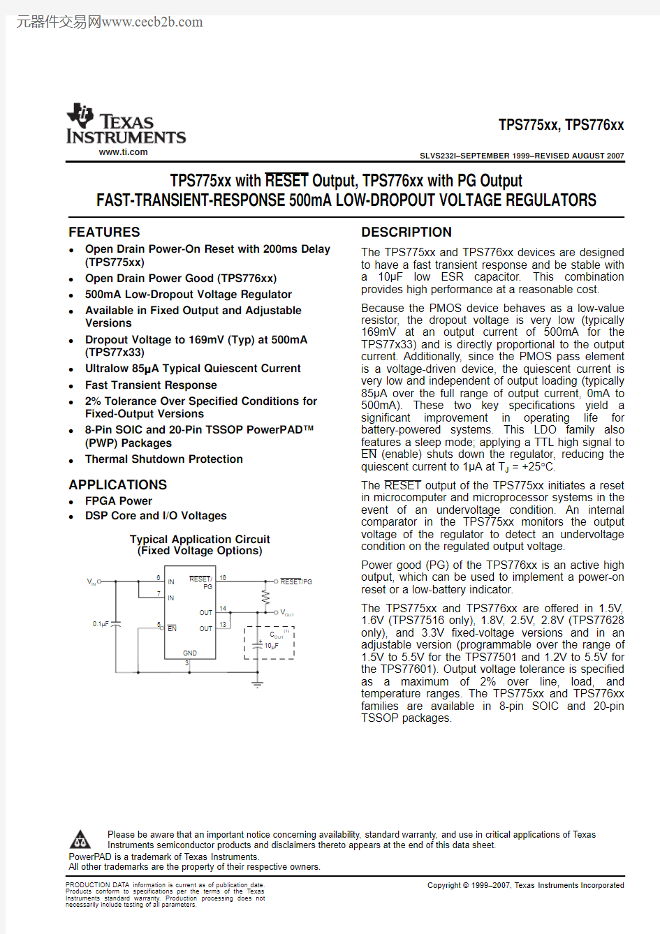
voltage of the regulator to detect an undervoltage Typical Application Circuit condition on the regulated output voltage.
(Fixed Voltage Options)
Power good(PG)of the TPS776xx is an active high
output,which can be used to implement a power-on
reset or a low-battery indicator.
The TPS775xx and TPS776xx are offered in1.5V,
1.6V(TPS77516only),1.8V,
2.5V,2.8V(TPS77628
only),and 3.3V fixed-voltage versions and in an
adjustable version(programmable over the range of
1.5V to5.5V for the TPS77501and1.2V to5.5V for
the TPS77601).Output voltage tolerance is specified
as a maximum of2%over line,load,and
temperature ranges.The TPS775xx and TPS776xx
families are available in8-pin SOIC and20-pin
TSSOP packages.
Please be aware that an important notice concerning availability,standard warranty,and use in critical applications of Texas
Instruments semiconductor products and disclaimers thereto appears at the end of this data sheet.
PowerPAD is a trademark of Texas Instruments.
https://www.360docs.net/doc/c32917912.html,
ABSOLUTE MAXIMUM RATINGS
DISSIPATION RATINGS
TPS775xx,TPS776xx
SLVS232I–SEPTEMBER 1999–REVISED AUGUST 2007
This integrated circuit can be damaged by ESD.Texas Instruments recommends that all integrated circuits be handled with appropriate precautions.Failure to observe proper handling and installation procedures can cause damage.
ESD damage can range from subtle performance degradation to complete device failure.Precision integrated circuits may be more susceptible to damage because very small parametric changes could cause the device not to meet its published specifications.
ORDERING INFORMATION (1)
PRODUCT
V OUT (2)
TPS775xx yyyz ,TPS776xx yyyz
XX is nominal output voltage (for example,28=2.8V,285=2.85V,01=Adjustable).YYY is package designator.Z is package quantity.
(1)For the most current package and ordering information see the Package Option Addendum at the end of this document,or see the TI website at https://www.360docs.net/doc/c32917912.html, .
(2)Custom fixed output voltages are available;minimum order quantities may apply.Contact factory for details and availability.
Over operating temperature range (unless otherwise noted)(1)
PARAMETER
TPS775xx,TPS776xx
UNIT Input voltage range,V IN (2)
–0.3to +13.5V Voltage range at EN
–0.3to +16.5
V Maximum RESET voltage (TPS775xx)16.5V Maximum PG voltage (TPS776xx)16.5V Peak output current Internally limited
Voltage range at OUT,FB 7
V Continuous total power dissipation See Dissipation Ratings Table Operating junction temperature range,T J –40to +125°C Storage junction temperature range ,T STG –65to +150
°C ESD rating,HBM 2
kV
(1)Stresses above these ratings may cause permanent damage to the device.Exposure to absolute maximum conditions for extended periods may degrade device reliability.These are stress ratings only,and functional operation of the device at these or any other conditions beyond those specified is not implied.
(2)
All voltages are with respect to network terminal ground.
AIRFLOW DERATING FACTOR BOARD PACKAGE
(CFM)
T A <+25°C ABOVE T A =+25°C
T A =+70°C T A =+85°C 0568mW 5.68mW/°C 312mW 227mW —D 250904mW 9.04mW/°C 497mW 361mW 0 2.9mW 23.5mW/°C 1.9W 1.5W Low-K (1)PWP 300 4.3mW 34.6mW/°C 2.8W 2.2W 03W 23.8mW/°C 1.9W 1.5W High-K (2)PWP
300
7.2W
57.9mW/°C
4.6W
3.8W
(1)This parameter is measured with the recommended copper heat sink pattern on a 1-layer,5in ?5in printed circuit board (PCB),1-ounce copper,2in ?2in coverage (4in 2).
(2)
This parameter is measured with the recommended copper heat sink pattern on a 8-layer,1.5in ?2in PCB,1-ounce copper with layers 1,2,4,5,7,and 8at 5%coverage (0.9in 2)and layers 3and 6at 100%coverage (6in 2).For more information,refer to TI technical brief SLMA002.
https://www.360docs.net/doc/c32917912.html,
ELECTRICAL CHARACTERISTICS
TPS775xx,TPS776xx SLVS232I–SEPTEMBER1999–REVISED AUGUST2007
Over recommended operating temperature range(T J=–40°C to+125°C),V IN=V OUT(TYP)+1V;I OUT=1mA,V EN=0V,C OUT= 10μF,unless otherwise noted.Typical values are at T J=+25°C.
PARAMETER TEST CONDITIONS MIN TYP MAX UNIT
V IN Input voltage range 2.710V
TPS77501 1.5 5.5V V OUT Output voltage range
TPS77601 1.2 5.5V
V OUT+1V≤V IN≤10V(1)
V OUT Accuracy–2.0+2.0%
10μA
I OUT=10mA85
I GND Ground pin currentμA
I OUT=500mA125
ΔV OUT%/ΔV IN Output voltage line regulation V OUT+1V≤V IN≤10V(1)0.01%/V ΔV OUT%/ΔI OUT Load regulation3mV
Output noise voltage
V N TPS77x18I C=500mA,C OUT=10μF53μV RMS BW=200Hz to100kHz
TPS77628I OUT=500mA285410mV V DO Dropout voltage(2)TPS77533I OUT=500mA169287mV
TPS77633I OUT=500mA169287mV
I CL Output current limit V OUT=0V 1.2 1.6 1.9A
T SD Shutdown temperature150°C T J Operating junction temperature range–40+125°C
EN=V IN,at T J=+25°C,
1
2.7V I STBY Standby currentμA EN=V IN,2.7V I FB FB input current TPS77x01FB=1.5V2nA V EN(HI)High-level enable input voltage 1.7V V EN(LO)Low-level enable input voltage0.9V PSRR Power-supply ripple rejection f=100Hz,C OUT=10μF60dB Minimum input voltage for valid RESET I OUT(RESET)=300μA 1.1V Trip threshold voltage V OUT decreasing9298%V OUT Hysteresis voltage Measured at V OUT0.5%V OUT RESET (TPS775xx)Output low voltage V IN =2.7V,I OUT(RESET)=1mA0.150.4V Leakage current V(RESET)=5V1μA RESET time-out delay200ms Minimum input voltage for valid PG I OUT(PG)=300μA 1.1V Trip threshold voltage V OUT decreasing9298%V OUT PG Hysteresis voltage Measured at V OUT0.5%V OUT (TPS776xx) Output low voltage V IN=2.7V,I OUT(PG)=1mA0.150.4V Leakage current V(PG)=5V1μA EN=0V–101 Input current(EN)μA EN=V IN–11 (1)Minimum V IN=V OUT+V DO or2.7V,whichever is greater. (2)V DO is not measured for fixed output versions with V OUT(NOM)<2.8V because mimimum V IN=2.7V. https://www.360docs.net/doc/c32917912.html, FUNCTIONAL BLOCK DIAGRAMS External to the device GND OUT PG or RESET TPS775xx,TPS776xx SLVS232I–SEPTEMBER 1999–REVISED AUGUST 2007 Adjustable Voltage Versions Fixed Voltage Versions https://www.360docs.net/doc/c32917912.html, PIN CONFIGURATIONS GND/HSINK GND/HSINK NC NC FB/NC OUT OUT GND/HSINK GND/HSINK GND/HSINK GND/HSINK GND NC EN IN IN NC GND/HSINK GND/HSINK RESET/PG TPS775xx,TPS776xx SLVS232I–SEPTEMBER 1999–REVISED AUGUST 2007 TSSOP-20SOIC-8PWP D (TOP VIEW) (TOP VIEW) Table 1.PIN DESCRIPTIONS TPS775xx,TPS776xx TSSOP-20SOIC-8(D)(PWP)NAME PIN NO. PIN NO. DESCRIPTION EN 25Negative polarity enable (EN)input Adjustable voltage version only;feedback voltage for setting output voltage of the device.FB 715 Not internally connected on adjustable versions. 1,2,3,9,10, GND 111,12,19,Ground 20 IN 3,46,7Input voltage OUT 5,613,14Regulated output voltage RESET 816TPS775xx devices only;open-drain RESET output. PG 816TPS776xx devices only;open-drain power-good (PG)output.NC —4,8,17,18 No internal connection PAD/TAB — — Should be soldered to ground plane and used for heat sinking. https://www.360docs.net/doc/c32917912.html, V V IN TYPICAL CHARACTERISTICS TPS775xx,TPS776xx SLVS232I–SEPTEMBER 1999–REVISED AUGUST 2007 TPS775xx RESET Timing Diagram (1)V res is res standards for semiconductor symbology. (2) V IT :Trip voltage is typically 5%lower than the output voltage (95%V OUT ).V IT–to V IT+is the hysteresis voltage. Table of Graphs FIGURE NO. vs Output Current Figure 3,Figure 4,Figure 5V OUT Output Voltage vs Free-Air Temperature Figure 6,Figure 7,Figure 8 vs Time Figure 20I GND Ground Current vs Free-Air Temperature Figure 9PSRR Power-Supply Ripple Rejection vs Frequency Figure 10Output Spectral Noise Density vs Frequency Figure 11Z OUT Output Impedance vs Frequency Figure 12vs Input Voltage Figure 13V DO Dropout Voltage vs Free-Air Temperature Figure 14V IN Input Voltage (Min)vs Output Voltage Figure 15LINE Line Transient Response Figure 16,Figure 18LOAD Load Transient Response Figure 17,Figure 19ESR Equivalent Series Resistance vs Output Current Figure 22,Figure 23 https://www.360docs.net/doc/c32917912.html, TYPICAL CHARACTERISTICS 3.28303.28153.2800 3.28253.2820 3.28103.2835 3.2805V O u t p u t V o l t a g e V -O U T -0.2 0.3 0.4 0.5 0.0 0.1 I OUT --Output Current A 1.4980 1.4965 1.4950 1.4975 1.4970 1.4960 1.4985 1.4955 V O u t p u t V o l t a g e V -O U T -0.2 0.3 0.4 0.5 0.0 0.1 I OUT --Output Current A 2.49552.49402.4920 2.4950 2.49452.49352.49602.4930 2.4925V O u t p u t V o l t a g e V -O U T -0.20.30.40.5 0.00.1I OUT --Output Current A 3.31 3.28 3.25 -40 03.30 3.29 3.27 -20100140 3.32 -601203.26 204060 80V O u t p u t V o l t a g e V -O U T -T A --Free-Air T emperature C °TPS775xx,TPS776xx SLVS232I–SEPTEMBER 1999–REVISED AUGUST 2007 Over operating temperature range (T J =–40°C to +125°C)unless otherwise noted.Typical values are at T J =+25°C. TPS77x33 TPS77x15 OUTPUT VOLTAGE OUTPUT VOLTAGE vs OUTPUT CURRENT vs OUTPUT CURRENT Figure 3. Figure 4. TPS77x25 TPS77x33 OUTPUT VOLTAGE OUTPUT VOLTAGE vs OUTPUT CURRENT vs FREE-AIR TEMPERATURE Figure 5.Figure 6. https://www.360docs.net/doc/c32917912.html, 1.515 1.500 1.485 1.510 1.505 1.495 1.490 V O u t p u t V o l t a g e V -O U T --40 -20 100 140 -60120 20 40 60 80 T A --Free-Air T emperature C ° 2.515 2.500 2.480 2.5102.505 2.495 2.490 2.485 -40 -20 100 140 -60120 20 40 60 80 T A --Free-Air T emperature C °V O u t p u t V o l t a g e V -O U T -100 95 90 85 80 75 G r o u n d C u r r e n t A m --40 0-20100140 -6012020406080T A --Free-Air T emperature C °6050403020100 -10 90 80P S R R P o w e r S u p p l y R i p p l e R e j e c t i o n d B --10 10 10 10 10 10 6 f --Frequency Hz 70TPS775xx,TPS776xx SLVS232I–SEPTEMBER 1999–REVISED AUGUST 2007 TYPICAL CHARACTERISTICS (continued) Over operating temperature range (T J =–40°C to +125°C)unless otherwise noted.Typical values are at T J =+25°C. TPS77x15 TPS77x25 OUTPUT VOLTAGE OUTPUT VOLTAGE vs FREE-AIR TEMPERATURE vs FREE-AIR TEMPERATURE Figure 7. Figure 8. TPS77xxx TPS77x33 GROUND CURRENT POWER-SUPPLY RIPPLE REJECTION vs FREE-AIR TEMPERATURE vs FREQUENCY Figure 9.Figure 10. https://www.360docs.net/doc/c32917912.html, 10 10 10 10 5 10 -5 10 -6 10 -7 f --Frequency Hz 10 -8 O u t p u t S p e c t r a l N o i s e D e n s i t y V /m -H z ?10 1 10 2 10 10 4 10 5 10 6 f --Frequency Hz 10 -1 10 -2 10 Z O u t p u t I m p e d a n c e -W O U T -300 150 0250 200 100 2.5 50 V D r o p o u t V o l t a g e V -D O -m 350 V IN --Input Voltage V 3.0 3.5 4.0 4.5 5.0 -400-20100140 -6012020406080T A --Free-Air T emperature C °V D r o p o u t V o l t a g e V -D O -m 10 1 10 -1 10 2 10 10 -2 10 3 TPS775xx,TPS776xx SLVS232I–SEPTEMBER 1999–REVISED AUGUST 2007 TYPICAL CHARACTERISTICS (continued) Over operating temperature range (T J =–40°C to +125°C)unless otherwise noted.Typical values are at T J =+25°C. TPS77x33 TPS77x33 OUTPUT SPECTRAL NOISE DENSITY OUTPUT IMPEDANCE vs FREQUENCY vs FREQUENCY Figure 11.Figure 12. TPS77x01 TPS77x33 DROPOUT VOLTAGE DROPOUT VOLTAGE vs INPUT VOLTAGE vs FREE-AIR TEMPERATURE Figure 13.Figure 14. https://www.360docs.net/doc/c32917912.html, 1003.7 2.7 020406080100120140160180200 t --Time s V O U T --C h a n g e i n O u t p u t V o l t a g e m V -10 V I n p u t V o l t a g e V -I N -3 2.7 21.50 1.75 2.0 2.25 2.50 2.754 3.0 3.25 3.5 V I n p u t V o l t a g e V -I N -V OUT --Output Voltage V 500 500V O U T --C h a n g e i n O u t p u t V o l t a g e m V -50 0204060 80100120140160 180200t --Time s I O u t p u t C u r r e n t m A -O U T - 020406080100120140160180200 t --Time s 1005.3 4.3 V O U T --C h a n g e i n O u t p u t V o l t a g e m V -10 V I n p u t V o l t a g e V -I N -TPS775xx,TPS776xx SLVS232I–SEPTEMBER 1999–REVISED AUGUST 2007 TYPICAL CHARACTERISTICS (continued) Over operating temperature range (T J =–40°C to +125°C)unless otherwise noted.Typical values are at T J =+25°C. INPUT VOLTAGE (MIN)TPS77x15 vs OUTPUT VOLTAGE LINE TRANSIENT RESPONSE Figure 15. Figure 16. TPS77x15 TPS77x33 LOAD TRANSIENT RESPONSE LINE TRANSIENT RESPONSE Figure 17.Figure 18. https://www.360docs.net/doc/c32917912.html, 020406080100120140160180200 t --Time s 5000 500V O U T --C h a n g e i n O u t p u t V o l t a g e m V -50 I O u t p u t C u r r e n t m A -O U T -320 1 400.10.20.30.40.50.60.70.80.9 1.0 t --Time ms V O U T --O u t p u t V o l t a g e V E n a b l e P u l s e V -TPS775xx,TPS776xx SLVS232I–SEPTEMBER 1999–REVISED AUGUST 2007 TYPICAL CHARACTERISTICS (continued) Over operating temperature range (T J =–40°C to +125°C)unless otherwise noted.Typical values are at T J =+25°C. TPS77x33 TPS77x33OUTPUT VOLTAGE LOAD TRANSIENT RESPONSE vs TIME (AT STARTUP) Figure 19.Figure 20. https://www.360docs.net/doc/c32917912.html, V 0.1 10 1 0.01 I OUT-- Output Current mA 100200300400500 E S R E q u i v a l e n t S e r i e s R e s i s t a n c e - - 10 0.1 1 0.01 I OUT-- Output Current mA 100200300400500 E S R E q u i v a l e n t S e r i e s R e s i s t a n c e - - TPS775xx,TPS776xx SLVS232I–SEPTEMBER1999–REVISED AUGUST2007 TYPICAL CHARACTERISTICS(continued) Over operating temperature range(T J=–40°C to+125°C)unless otherwise noted.Typical values are at T J=+25°C. Test Circuit for Typical Regions of Stability(Figure22and Figure23)(Fixed Output Options) Figure21. TYPICAL REGION OF STABILITY TYPICAL REGION OF STABILITY EQUIVALENT SERIES RESISTANCE(1)EQUIVALENT SERIES RESISTANCE(1) vs OUTPUT CURRENT vs OUTPUT CURRENT (1)Equivalent series resistance(ESR)refers to(1)Equivalent series resistance(ESR)refers to the total series resistance,including the the total series resistance,including the ESR of the capacitor,any series resistance ESR of the capacitor,any series resistance added externally,and PWB trace resistance added externally,and PWB trace resistance to C OUT.to C OUT. Figure22.Figure23. https://www.360docs.net/doc/c32917912.html, APPLICATION INFORMATION Minimum Load Requirements FB—Pin Connection(Adjustable Version Only) External Capacitor Requirements V TPS775xx,TPS776xx SLVS232I–SEPTEMBER1999–REVISED AUGUST2007 The TPS775xx and TPS776xx feature very low quiescent current,which remains virtually constant even with varying loads.Conventional LDO regulators use a pnp pass element,the base current of which is directly proportional to the load current through the regulator(I B=I C/β).The TPS775xx and TPS776xx use a PMOS transistor to pass current;because the gate of the PMOS is voltage driven,operating current is low and invariable over the full load range. Another pitfall associated with the pnp-pass element is its tendency to saturate when the device goes into dropout.The resulting drop inβforces an increase in I B to maintain the load.During power up,this I B increase translates to large start-up currents.Systems with limited supply current may fail to start up.In battery-powered systems,it means rapid battery discharge when the voltage decays below the minimum required for regulation. The TPS775xx and TPS776xx quiescent currents remain low even when the regulator drops out,eliminating both problems. The TPS775xx and TPS776xx families also feature a shutdown mode that places the output in the high-impedance state(essentially equal to the feedback-divider resistance)and reduces quiescent current to 2μA.If the shutdown feature is not used,EN should be tied to ground. The TPS775xx and TPS776xx families are stable at zero load;no minimum load is required for operation. The FB pin is an input pin to sense the output voltage and close the loop for the adjustable option.The output voltage is sensed through a resistor divider network to close the loop as it is shown in Figure25.Normally,this connection should be as short as possible;however,the connection can be made near a critical circuit to improve performance at that point.Internally,FB connects to a high-impedance wide-bandwidth amplifier and noise pickup feeds through to the regulator output.Routing the FB connection to minimize/avoid noise pickup is essential. An input capacitor is not usually required;however,a ceramic bypass capacitor(0.047μF or larger)improves load transient response and noise rejection if the TPS775xx or TPS776xx are located more than a few inches from the power supply.A higher-capacitance electrolytic capacitor may be necessary if large(hundreds of milliamps)load transients with fast rise times are anticipated. Like all low dropout regulators,the TPS775xx and TPS776xx require an output capacitor connected between OUT and GND to stabilize the internal control loop.The minimum recommended capacitance value is10μF and the ESR(equivalent series resistance)must be between50m?and1.5?.Capacitor values10μF or larger are acceptable,provided the ESR is less than1.5?.Solid tantalum electrolytic,aluminum electrolytic,and multilayer ceramic capacitors are all suitable,provided they meet the requirements described previously. Figure24.Typical Application Circuit(Fixed Versions) https://www.360docs.net/doc/c32917912.html, Programming the TPS77x01Adjustable LDO Regulator V = V x (1 + ) OUT ref R R 1 2 (1) V V OUT ref 1) x R -2 R = ( 1(2) OUT >OUTPUT VOLTAGE PROGRAMMING GUIDE R 1R 2UNIT OUTPUT VOLTAGE 2.5V 3.3V 3.6V 4.75V 121196226332 110110110110 k W k W k W k W Reset Indicator Power-Good Indicator TPS775xx,TPS776xx SLVS232I–SEPTEMBER 1999–REVISED AUGUST 2007 APPLICATION INFORMATION (continued) The output voltage of the TPS77x01adjustable regulator is programmed using an external resistor divider as shown in Figure 25.The output voltage is calculated using Equation 1: Where: ? V ref =1.1834V typ (the internal reference voltage) Resistors R 1and R 2should be chosen for approximately 10μA divider current.Lower value resistors can be used,but offer no inherent advantage and waste more power.Higher values should be avoided as leakage currents at FB increase the output voltage error.The recommended design procedure is to choose R 2=110k ?to set the divider current at approximately 10μA and then calculate R 1using Equation 2: Figure 25.TPS77x01Adjustable LDO Regulator Programming The TPS775xx features a RESET output that can be used to monitor the status of the regulator.The internal comparator monitors the output voltage:when the output drops to between 92%and 98%of its nominal regulated value,the RESET output transistor turns on,taking the signal low.The open-drain output requires a pullup resistor.If not used,it can be left floating.RESET can be used to drive power-on reset circuitry or as a low-battery indicator.RESET does not assert itself when the regulated output voltage falls outside the specified 2%tolerance,but instead reports an output voltage low relative to its nominal regulated value (refer to Timing Diagram for start-up sequence). The TPS776xx features a power-good (PG)output that can be used to monitor the status of the regulator.The internal comparator monitors the output voltage:when the output drops to between 92%and 98%of its nominal regulated value,the PG output transistor turns on,taking the signal low.The open-drain output requires a pullup resistor.If not used,it can be left floating.PG can be used to drive power-on reset circuitry or used as a low-battery indicator. https://www.360docs.net/doc/c32917912.html, Regulator Protection Power Dissipation and Junction Temperature P = D(max)R q JA T J(max)T -A 1 derating factor from the dissipation rating tables P = (V V ) x I -D IN OUT OUT TPS775xx,TPS776xx SLVS232I–SEPTEMBER 1999–REVISED AUGUST 2007 APPLICATION INFORMATION (continued) The TPS775xx and TPS776xx PMOS-pass transistors have a built-in back diode that conducts reverse currents when the input voltage drops below the output voltage (for example,during power down).Current is conducted from the output to the input and is not internally limited.When extended reverse voltage is anticipated,external limiting may be appropriate. The TPS775xx and TPS776xx also feature internal current limiting and thermal protection.During normal operation,the TPS775xx and TPS776xx limit output current to approximately 1.7A.When current limiting engages,the output voltage scales back linearly until the overcurrent condition ends.While current limiting is designed to prevent gross device failure,care should be taken not to exceed the power dissipation ratings of the package.If the temperature of the device exceeds +150°C(typ),thermal-protection circuitry shuts it down.Once the device has cooled below +130°C(typ),regulator operation resumes. Specified regulator operation is assured to a junction temperature of +125°C;the maximum junction temperature should be restricted to +125°C under normal operating conditions.This restriction limits the power dissipation the regulator can handle in any given application.To ensure the junction temperature is within acceptable limits,calculate the maximum allowable dissipation,P D(max),and the actual dissipation,P D ,which must be less than or equal to P D(max). The maximum-power-dissipation limit is determined using the following equation: where: ?T J(max)is the maximum allowable junction temperature ? R θJA is the thermal resistance junction-to-ambient for the package,and is calculated as ? T A is the ambient temperature The regulator dissipation is calculated using: Power dissipation resulting from quiescent current is negligible.Excessive power dissipation will trigger the thermal protection circuit. PACKAGING INFORMATION Orderable Device Status (1)Package Type Package Drawing Pins Package Qty Eco Plan (2) Lead/Ball Finish MSL Peak Temp (3)TPS77501D ACTIVE SOIC D 875Green (RoHS &no Sb/Br)CU NIPDAU Level-1-260C-UNLIM TPS77501DG4ACTIVE SOIC D 875 Green (RoHS &no Sb/Br) CU NIPDAU Level-1-260C-UNLIM TPS77501DR ACTIVE SOIC D 82500Green (RoHS & no Sb/Br)CU NIPDAU Level-1-260C-UNLIM TPS77501DRG4ACTIVE SOIC D 82500Green (RoHS & no Sb/Br)CU NIPDAU Level-1-260C-UNLIM TPS77501PWP ACTIVE HTSSOP PWP 2070Green (RoHS &no Sb/Br)CU NIPDAU Level-2-260C-1YEAR TPS77501PWPG4ACTIVE HTSSOP PWP 2070 Green (RoHS &no Sb/Br) CU NIPDAU Level-2-260C-1YEAR TPS77501PWPR ACTIVE HTSSOP PWP 202000Green (RoHS & no Sb/Br)CU NIPDAU Level-2-260C-1YEAR TPS77501PWPRG4 ACTIVE HTSSOP PWP 202000Green (RoHS & no Sb/Br)CU NIPDAU Level-2-260C-1YEAR TPS77515D ACTIVE SOIC D 875Green (RoHS &no Sb/Br)CU NIPDAU Level-1-260C-UNLIM TPS77515DG4ACTIVE SOIC D 875 Green (RoHS &no Sb/Br) CU NIPDAU Level-1-260C-UNLIM TPS77515DR ACTIVE SOIC D 82500Green (RoHS & no Sb/Br)CU NIPDAU Level-1-260C-UNLIM TPS77515DRG4ACTIVE SOIC D 82500Green (RoHS & no Sb/Br)CU NIPDAU Level-1-260C-UNLIM TPS77515PWP ACTIVE HTSSOP PWP 2070Green (RoHS &no Sb/Br)CU NIPDAU Level-2-260C-1YEAR TPS77515PWPG4ACTIVE HTSSOP PWP 2070 Green (RoHS &no Sb/Br) CU NIPDAU Level-2-260C-1YEAR TPS77515PWPR ACTIVE HTSSOP PWP 202000Green (RoHS & no Sb/Br)CU NIPDAU Level-2-260C-1YEAR TPS77515PWPRG4 ACTIVE HTSSOP PWP 202000Green (RoHS & no Sb/Br)CU NIPDAU Level-2-260C-1YEAR TPS77516D ACTIVE SOIC D 875Green (RoHS &no Sb/Br)CU NIPDAU Level-1-260C-UNLIM TPS77516DG4ACTIVE SOIC D 875 Green (RoHS &no Sb/Br) CU NIPDAU Level-1-260C-UNLIM TPS77516DR ACTIVE SOIC D 82500Green (RoHS & no Sb/Br)CU NIPDAU Level-1-260C-UNLIM TPS77516DRG4ACTIVE SOIC D 82500Green (RoHS & no Sb/Br)CU NIPDAU Level-1-260C-UNLIM TPS77516PWP ACTIVE HTSSOP PWP 2070Green (RoHS &no Sb/Br)CU NIPDAU Level-2-260C-1YEAR TPS77516PWPG4ACTIVE HTSSOP PWP 2070 Green (RoHS &no Sb/Br) CU NIPDAU Level-2-260C-1YEAR TPS77516PWPR ACTIVE HTSSOP PWP 202000Green (RoHS & no Sb/Br)CU NIPDAU Level-2-260C-1YEAR TPS77516PWPRG4 ACTIVE HTSSOP PWP 202000Green (RoHS & no Sb/Br)CU NIPDAU Level-2-260C-1YEAR TPS77518D ACTIVE SOIC D 8 75 Green (RoHS &no Sb/Br) CU NIPDAU Level-1-260C-UNLIM https://www.360docs.net/doc/c32917912.html, 19-Jun-2007 Orderable Device Status (1)Package Type Package Drawing Pins Package Qty Eco Plan (2) Lead/Ball Finish MSL Peak Temp (3)TPS77518DG4ACTIVE SOIC D 875 Green (RoHS &no Sb/Br) CU NIPDAU Level-1-260C-UNLIM TPS77518DR ACTIVE SOIC D 82500Green (RoHS & no Sb/Br)CU NIPDAU Level-1-260C-UNLIM TPS77518DRG4ACTIVE SOIC D 82500Green (RoHS & no Sb/Br)CU NIPDAU Level-1-260C-UNLIM TPS77518PWP ACTIVE HTSSOP PWP 2070Green (RoHS &no Sb/Br)CU NIPDAU Level-2-260C-1YEAR TPS77518PWPG4ACTIVE HTSSOP PWP 2070 Green (RoHS &no Sb/Br) CU NIPDAU Level-2-260C-1YEAR TPS77518PWPR ACTIVE HTSSOP PWP 202000Green (RoHS & no Sb/Br)CU NIPDAU Level-2-260C-1YEAR TPS77518PWPRG4 ACTIVE HTSSOP PWP 202000Green (RoHS & no Sb/Br)CU NIPDAU Level-2-260C-1YEAR TPS77525D ACTIVE SOIC D 875Green (RoHS &no Sb/Br)CU NIPDAU Level-1-260C-UNLIM TPS77525DG4ACTIVE SOIC D 875 Green (RoHS &no Sb/Br) CU NIPDAU Level-1-260C-UNLIM TPS77525DR ACTIVE SOIC D 82500Green (RoHS & no Sb/Br)CU NIPDAU Level-1-260C-UNLIM TPS77525DRG4ACTIVE SOIC D 82500Green (RoHS & no Sb/Br)CU NIPDAU Level-1-260C-UNLIM TPS77525PWP ACTIVE HTSSOP PWP 2070Green (RoHS &no Sb/Br)CU NIPDAU Level-2-260C-1YEAR TPS77525PWPG4ACTIVE HTSSOP PWP 2070 Green (RoHS &no Sb/Br) CU NIPDAU Level-2-260C-1YEAR TPS77525PWPR ACTIVE HTSSOP PWP 202000Green (RoHS & no Sb/Br)CU NIPDAU Level-2-260C-1YEAR TPS77525PWPRG4 ACTIVE HTSSOP PWP 202000Green (RoHS & no Sb/Br)CU NIPDAU Level-2-260C-1YEAR TPS77533D ACTIVE SOIC D 875Green (RoHS &no Sb/Br)CU NIPDAU Level-1-260C-UNLIM TPS77533DG4ACTIVE SOIC D 875 Green (RoHS &no Sb/Br) CU NIPDAU Level-1-260C-UNLIM TPS77533DR ACTIVE SOIC D 82500Green (RoHS & no Sb/Br)CU NIPDAU Level-1-260C-UNLIM TPS77533DRG4ACTIVE SOIC D 82500Green (RoHS & no Sb/Br)CU NIPDAU Level-1-260C-UNLIM TPS77533PWP ACTIVE HTSSOP PWP 2070Green (RoHS &no Sb/Br)CU NIPDAU Level-2-260C-1YEAR TPS77533PWPG4ACTIVE HTSSOP PWP 2070 Green (RoHS &no Sb/Br) CU NIPDAU Level-2-260C-1YEAR TPS77533PWPR ACTIVE HTSSOP PWP 202000Green (RoHS & no Sb/Br)CU NIPDAU Level-2-260C-1YEAR TPS77533PWPRG4 ACTIVE HTSSOP PWP 202000Green (RoHS & no Sb/Br)CU NIPDAU Level-2-260C-1YEAR TPS77601D ACTIVE SOIC D 875Green (RoHS &no Sb/Br)CU NIPDAU Level-1-260C-UNLIM TPS77601DG4ACTIVE SOIC D 875 Green (RoHS &no Sb/Br) CU NIPDAU Level-1-260C-UNLIM TPS77601DR ACTIVE SOIC D 8 2500Green (RoHS & no Sb/Br) CU NIPDAU Level-1-260C-UNLIM https://www.360docs.net/doc/c32917912.html, 19-Jun-2007 Orderable Device Status (1)Package Type Package Drawing Pins Package Qty Eco Plan (2) Lead/Ball Finish MSL Peak Temp (3)TPS77601DRG4ACTIVE SOIC D 82500Green (RoHS & no Sb/Br)CU NIPDAU Level-1-260C-UNLIM TPS77601PWP ACTIVE HTSSOP PWP 2070Green (RoHS &no Sb/Br)CU NIPDAU Level-2-260C-1YEAR TPS77601PWPG4ACTIVE HTSSOP PWP 2070 Green (RoHS &no Sb/Br) CU NIPDAU Level-2-260C-1YEAR TPS77601PWPR ACTIVE HTSSOP PWP 202000Green (RoHS & no Sb/Br)CU NIPDAU Level-2-260C-1YEAR TPS77601PWPRG4 ACTIVE HTSSOP PWP 202000Green (RoHS & no Sb/Br)CU NIPDAU Level-2-260C-1YEAR TPS77615D ACTIVE SOIC D 875Green (RoHS &no Sb/Br)CU NIPDAU Level-1-260C-UNLIM TPS77615DG4ACTIVE SOIC D 875 Green (RoHS &no Sb/Br) CU NIPDAU Level-1-260C-UNLIM TPS77615DR ACTIVE SOIC D 82500Green (RoHS & no Sb/Br)CU NIPDAU Level-1-260C-UNLIM TPS77615DRG4ACTIVE SOIC D 82500Green (RoHS & no Sb/Br)CU NIPDAU Level-1-260C-UNLIM TPS77615PWP ACTIVE HTSSOP PWP 2070Green (RoHS &no Sb/Br)CU NIPDAU Level-2-260C-1YEAR TPS77615PWPG4ACTIVE HTSSOP PWP 2070 Green (RoHS &no Sb/Br) CU NIPDAU Level-2-260C-1YEAR TPS77615PWPR ACTIVE HTSSOP PWP 202000Green (RoHS & no Sb/Br)CU NIPDAU Level-2-260C-1YEAR TPS77615PWPRG4 ACTIVE HTSSOP PWP 202000Green (RoHS & no Sb/Br)CU NIPDAU Level-2-260C-1YEAR TPS77618D ACTIVE SOIC D 875Green (RoHS &no Sb/Br)CU NIPDAU Level-1-260C-UNLIM TPS77618DG4ACTIVE SOIC D 875 Green (RoHS &no Sb/Br) CU NIPDAU Level-1-260C-UNLIM TPS77618DR ACTIVE SOIC D 82500Green (RoHS & no Sb/Br)CU NIPDAU Level-1-260C-UNLIM TPS77618DRG4ACTIVE SOIC D 82500Green (RoHS & no Sb/Br)CU NIPDAU Level-1-260C-UNLIM TPS77618PWP ACTIVE HTSSOP PWP 2070Green (RoHS &no Sb/Br)CU NIPDAU Level-2-260C-1YEAR TPS77618PWPG4ACTIVE HTSSOP PWP 2070 Green (RoHS &no Sb/Br) CU NIPDAU Level-2-260C-1YEAR TPS77618PWPR ACTIVE HTSSOP PWP 202000Green (RoHS & no Sb/Br)CU NIPDAU Level-2-260C-1YEAR TPS77618PWPRG4 ACTIVE HTSSOP PWP 202000Green (RoHS & no Sb/Br)CU NIPDAU Level-2-260C-1YEAR TPS77625D ACTIVE SOIC D 875Green (RoHS &no Sb/Br)CU NIPDAU Level-1-260C-UNLIM TPS77625DG4ACTIVE SOIC D 875 Green (RoHS &no Sb/Br) CU NIPDAU Level-1-260C-UNLIM TPS77625DR ACTIVE SOIC D 82500Green (RoHS & no Sb/Br)CU NIPDAU Level-1-260C-UNLIM TPS77625DRG4ACTIVE SOIC D 82500Green (RoHS & no Sb/Br)CU NIPDAU Level-1-260C-UNLIM TPS77625PWP ACTIVE HTSSOP PWP 20 70 Green (RoHS &no Sb/Br) CU NIPDAU Level-2-260C-1YEAR https://www.360docs.net/doc/c32917912.html, 19-Jun-2007 Orderable Device Status(1)Package Type Package Drawing Pins Package Qty Eco Plan(2)Lead/Ball Finish MSL Peak Temp(3) TPS77625PWPG4ACTIVE HTSSOP PWP2070Green(RoHS& no Sb/Br) CU NIPDAU Level-2-260C-1YEAR TPS77625PWPR ACTIVE HTSSOP PWP202000Green(RoHS& no Sb/Br) CU NIPDAU Level-2-260C-1YEAR TPS77625PWPRG4ACTIVE HTSSOP PWP202000Green(RoHS& no Sb/Br) CU NIPDAU Level-2-260C-1YEAR TPS77628D ACTIVE SOIC D875Green(RoHS& no Sb/Br) CU NIPDAU Level-1-260C-UNLIM TPS77628DG4ACTIVE SOIC D875Green(RoHS& no Sb/Br) CU NIPDAU Level-1-260C-UNLIM TPS77628DRG4ACTIVE SOIC D8TBD Call TI Call TI TPS77628PWP ACTIVE HTSSOP PWP2070Green(RoHS& no Sb/Br) CU NIPDAU Level-2-260C-1YEAR TPS77628PWPG4ACTIVE HTSSOP PWP2070Green(RoHS& no Sb/Br) CU NIPDAU Level-2-260C-1YEAR TPS77628PWPR ACTIVE HTSSOP PWP202000Green(RoHS& no Sb/Br) CU NIPDAU Level-2-260C-1YEAR TPS77628PWPRG4ACTIVE HTSSOP PWP202000Green(RoHS& no Sb/Br)CU NIPDAU Level-2-260C-1YEAR TPS77633D ACTIVE SOIC D875Green(RoHS& no Sb/Br) CU NIPDAU Level-1-260C-UNLIM TPS77633DG4ACTIVE SOIC D875Green(RoHS& no Sb/Br) CU NIPDAU Level-1-260C-UNLIM TPS77633DR ACTIVE SOIC D82500Green(RoHS& no Sb/Br) CU NIPDAU Level-1-260C-UNLIM TPS77633DRG4ACTIVE SOIC D82500Green(RoHS& no Sb/Br) CU NIPDAU Level-1-260C-UNLIM TPS77633PWP ACTIVE HTSSOP PWP2070Green(RoHS& no Sb/Br) CU NIPDAU Level-2-260C-1YEAR TPS77633PWPG4ACTIVE HTSSOP PWP2070Green(RoHS& no Sb/Br) CU NIPDAU Level-2-260C-1YEAR TPS77633PWPR ACTIVE HTSSOP PWP202000Green(RoHS& no Sb/Br) CU NIPDAU Level-2-260C-1YEAR TPS77633PWPRG4ACTIVE HTSSOP PWP202000Green(RoHS& no Sb/Br) CU NIPDAU Level-2-260C-1YEAR (1)The marketing status values are defined as follows: ACTIVE:Product device recommended for new designs. LIFEBUY:TI has announced that the device will be discontinued,and a lifetime-buy period is in effect. NRND:Not recommended for new designs.Device is in production to support existing customers,but TI does not recommend using this part in a new design. PREVIEW:Device has been announced but is not in production.Samples may or may not be available. OBSOLETE:TI has discontinued the production of the device. (2)Eco Plan-The planned eco-friendly classification:Pb-Free(RoHS),Pb-Free(RoHS Exempt),or Green(RoHS&no Sb/Br)-please check https://www.360docs.net/doc/c32917912.html,/productcontent for the latest availability information and additional product content details. TBD:The Pb-Free/Green conversion plan has not been defined. Pb-Free(RoHS):TI's terms"Lead-Free"or"Pb-Free"mean semiconductor products that are compatible with the current RoHS requirements for all6substances,including the requirement that lead not exceed0.1%by weight in homogeneous materials.Where designed to be soldered at high temperatures,TI Pb-Free products are suitable for use in specified lead-free processes. Pb-Free(RoHS Exempt):This component has a RoHS exemption for either1)lead-based flip-chip solder bumps used between the die and package,or2)lead-based die adhesive used between the die and leadframe.The component is otherwise considered Pb-Free(RoHS compatible)as defined above. Green(RoHS&no Sb/Br):TI defines"Green"to mean Pb-Free(RoHS compatible),and free of Bromine(Br)and Antimony(Sb)based flame retardants(Br or Sb do not exceed0.1%by weight in homogeneous material) https://www.360docs.net/doc/c32917912.html,19-Jun-2007 (3) MSL,Peak Temp.--The Moisture Sensitivity Level rating according to the JEDEC industry standard classifications,and peak solder temperature. Important Information and Disclaimer:The information provided on this page represents TI's knowledge and belief as of the date that it is provided.TI bases its knowledge and belief on information provided by third parties,and makes no representation or warranty as to the accuracy of such information.Efforts are underway to better integrate information from third parties.TI has taken and continues to take reasonable steps to provide representative and accurate information but may not have conducted destructive testing or chemical analysis on incoming materials and chemicals.TI and TI suppliers consider certain information to be proprietary,and thus CAS numbers and other limited information may not be available for release. In no event shall TI's liability arising out of such information exceed the total purchase price of the TI part(s)at issue in this document sold by TI to Customer on an annual basis. https://www.360docs.net/doc/c32917912.html, 19-Jun-2007