Cadence中Capture向Allegro中导入网表时的常见错误

一、Capture生成netlist的时候报错:
1.Unable to open c:\Cadence\PSD_14.2\tools\capture\allegro.cfg for reading. Please correct the above error(s) to proceed
错误解释:
allegro.cfg文件找不到或allegro.cfg文件不能打开,这个问题的根源是,有可能每台电脑上安装Allegro的的位置不一样,allegro.cfg 文件找不到是理所当然的。
处理办法:
点生成netlist,点setup,修改路径为capture\allegro.cfg所在路径,把allegro.cfg文件的位置选择你现在安装目录的文件位置。
2. Spawning... "C:\Cadence\PSD_15.1\tools\capture\pstswp.exe" -pst -d "F:\gcht\CC2430\Projects\mysch.dsn" -n
"C:\CADENCE\PSD_15.1\TOOLS\PROJECTS" -c
"C:\Cadence\PSD_15.1\tools\capture\allegro.cfg" -v 3 -j
"CC2430_DEMO"
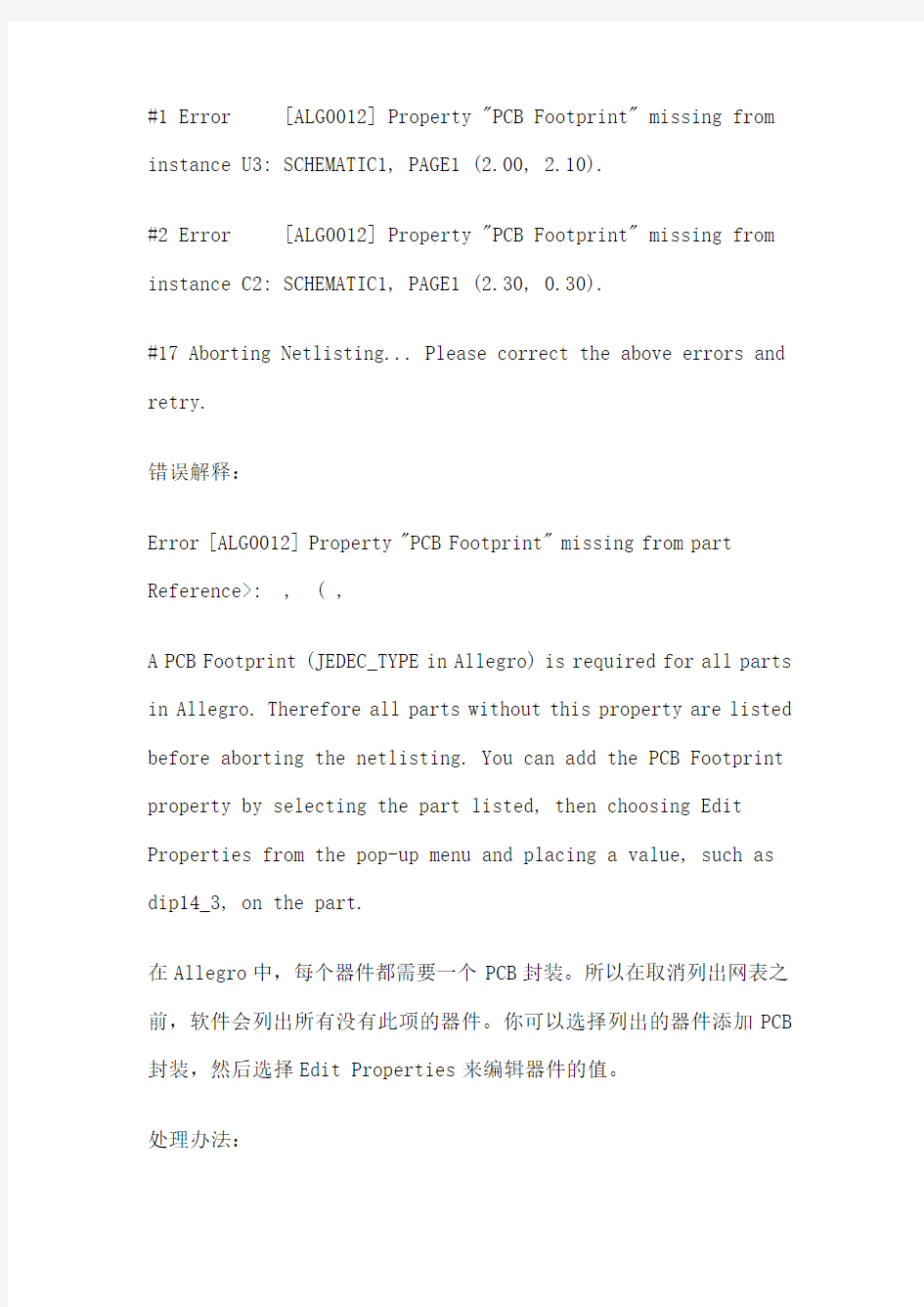
#1 Error [ALG0012] Property "PCB Footprint" missing from instance U3: SCHEMATIC1, PAGE1 (2.00, 2.10).
#2 Error [ALG0012] Property "PCB Footprint" missing from instance C2: SCHEMATIC1, PAGE1 (2.30, 0.30).
#17 Aborting Netlisting... Please correct the above errors and retry.
错误解释:
Error [ALG0012] Property "PCB Footprint" missing from part
A PC
B Footprint (JEDEC_TYPE in Allegro) is required for all parts in Allegro. Therefore all parts without this property are listed before aborting the netlisting. You can add the PCB Footprint property by selecting the part listed, then choosing Edit Properties from the pop-up menu and placing a value, such as dip14_3, on the part.
在Allegro中,每个器件都需要一个PCB封装。所以在取消列出网表之前,软件会列出所有没有此项的器件。你可以选择列出的器件添加PCB 封装,然后选择Edit Properties来编辑器件的值。
处理办法:
在导出Netlist 之前,只需要保证每个器件都是有封装的,且器件PCB Footprint值与对应的.dra封装文件名一致。
3. [DRC0011] Reference is invalid for this part
The reference for the part is invalid. For example, this occurs when a part reference like U?A has not been updated. Update the part reference。
Reference项不可随意修改。
4. Pin numbers do not match. Check device file.
原因:原理图中的晶振给了两个管脚,而其封装却是四个管脚。
原理图与PCB封装对应原则:
除了PCB Footprint的名字要写对以外,还有一点,就是原理图的元件的管脚数目一定要和封装的管脚数目必须一样。这里说的管脚,包括了原理图中可能没有现实的Power Pins,不包括封装中的machanical pins;另外,原理图和封装的对应关系是依靠pin number来建立的,所以两者的相应的pin number一定要一样,而pin number是不是数字并没有关系。
5. ERROR(SPMHNI-191): Device/Symbol check error detected. WARNING(SPMHNI-337): Unable to load symbol 'HDR1X2' for device 'B2S_HDR1X2_B2S': WARNING(SPMHUT-127): Could not find padstack 57S40DP.
due to ERROR(SPMHDB-274): Unable to load flash symbol THS79X59X45X4X15 (Check PSMPATH setting for this symbol)."
原因:花焊盘Flash没有创建.fsm的symbol文件,或是该文件保存路径与.psm文件不一致。
二、Allegro导入netlist的时候报错can not find symbol:
出现Netrev succeeded即可,说明已没有error了,可以直接打开自动生成的.brd文件了。但此时Updating Allegro PCB Editor Board
仍然会有红叉,貌似还有问题。果然,在QuickPlace的时候,有一些器件的Footprint无法Place,提示的错误原因是can not find symbol,不知所云。
有一种可能就是Allegro工作区的面积不够大,而QuickPlace放置的Footprint都位于Outline范围之外,因而如果工作区面积设置的不够大的话,会导致有一些器件的Footprint无法Place。
还有一种可能就是元件在原理图中的引脚数目与Footprint中的引脚数目不一致。这是也会出现Netrev succeeded,同时有警告,但是同样会导致这些器件的Footprint无法Place。
第三种可能:在导入Netlist时会产生如下警告:
WARNING(SPMHNI-192): Device/Symbol check warning detected.
WARNING(SPMHNI-337): Unable to load symbol '8P4R_0402_CN_42' for device 'RESARR_IS_4/SM_8P4R_0402_CN_4_1': WARNING(SPMHUT-127): Could not find padstack 8P4R-0402_CN-42_BIGPAD.
即找不到PAD文件。如果本身就没有PAD文件,则按照Datasheet上面引脚大小自己画一个;若有PAD文件,则应设置好路径:在PCB Editor 中Setup→User Preferences→Design_paths,设置padpath和psmpath;若对PAD文件进行过修改(包括重命名),则应在PCB Editor中Tools→Padstack,Replace或Refresh。
第四种可能:.dra封装文件有DRC错误。此时在生成网表时,在Capture 的Session Log中只会有Warning而无Error,但QuickPlace仍无法放置该Footprint。如何修改DRC错误。