74HC595D中文资料_数据手册_参数
74HC595; 74HCT595
8-bit serial-in, serial or parallel-out shift register with output
latches; 3-state
Rev. 6 — 12 December 2011Product data sheet
1. General description
The 74HC595; 74HCT595 are high-speed Si-gate CMOS devices and are pin compatible
with Low-power Schottky TTL (LSTTL). They are specified in compliance with JEDEC
standard No.7A.
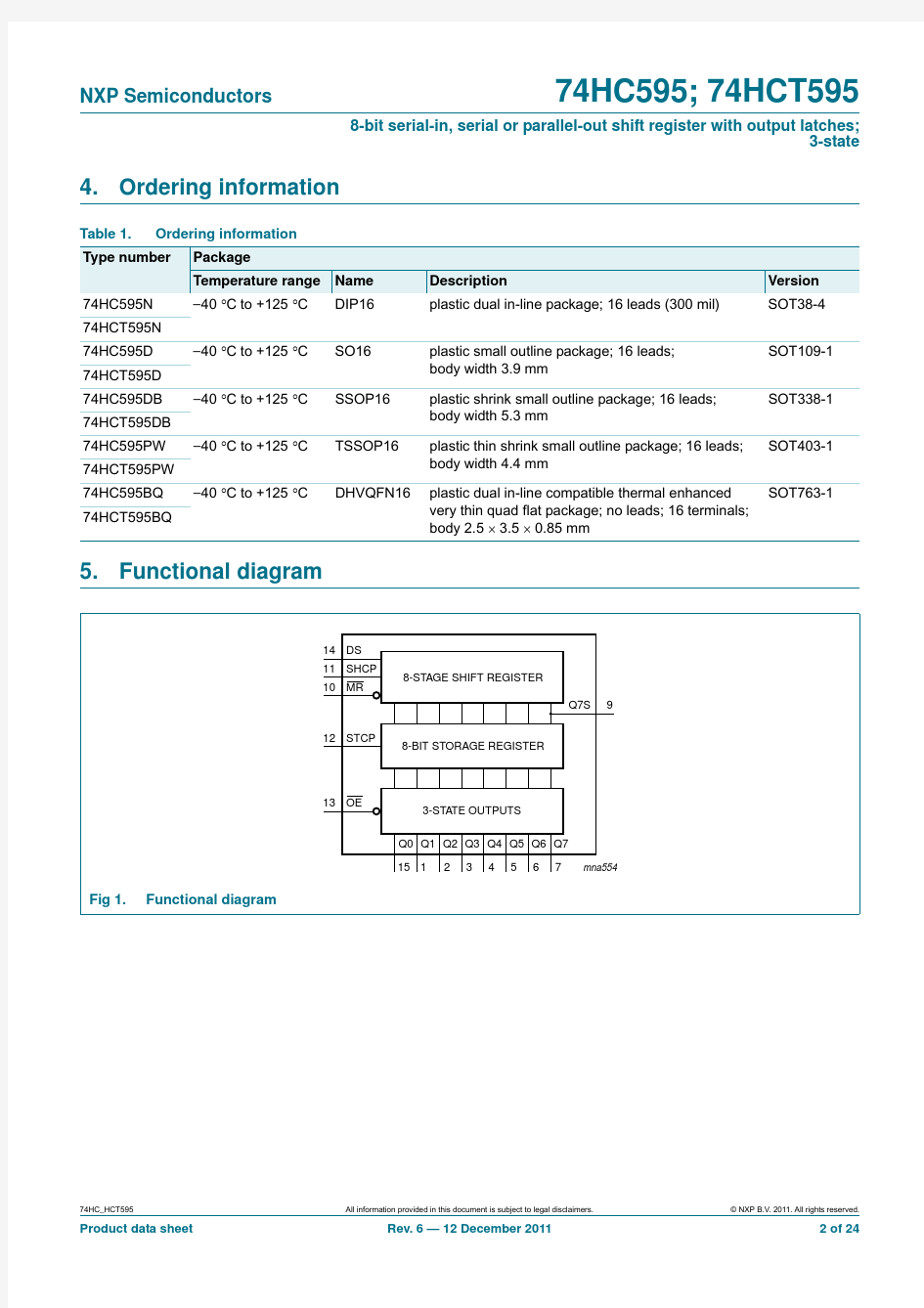
The 74HC595; 74HCT595 are 8-stage serial shift registers with a storage register and
3-state outputs. The registers have separate clocks.
Data is shifted on the positive-going transitions of the shift register clock input (SHCP).
The data in each register is transferred to the storage register on a positive-going
transition of the storage register clock input (STCP). If both clocks are connected together,
the shift register will always be one clock pulse ahead of the storage register.
The shift register has a serial input (DS) and a serial standard output (Q7S) for cascading.
It is also provided with asynchronous reset (active LOW) for all 8 shift register stages. The
storage register has 8 parallel 3-state bus driver outputs. Data in the storage register
appears at the output whenever the output enable input (OE) is LOW.
2. Features and benefits
?8-bit serial input
?8-bit serial or parallel output
?Storage register with 3-state outputs
?Shift register with direct clear
?100MHz (typical) shift out frequency
?ESD protection:
◆HBM JESD22-A114F exceeds2000V
◆MM JESD22-A115-A exceeds200V
?Multiple package options
?Specified from -40?C to+85?C and from -40?C to+125?C
3. Applications
?Serial-to-parallel data conversion
?Remote control holding register
3-state
4. Ordering information
5. Functional diagram
Table 1.
Ordering information
Type number
Package
Temperature range
Name Description
Version 74HC595N -40?C to +125?C
DIP16
plastic dual in-line package; 16leads (300mil)
SOT38-4
74HCT595N 74HC595D -40?C to +125?C
SO16
plastic small outline package; 16leads;
body width 3.9mm
SOT109-174HCT595D 74HC595DB -40?C to +125?C
SSOP16
plastic shrink small outline package; 16leads; body width 5.3mm
SOT338-174HCT595DB 74HC595PW -40?C to +125?C
TSSOP16
plastic thin shrink small outline package; 16leads; body width 4.4mm
SOT403-174HCT595PW 74HC595BQ -40?C to +125?C
DHVQFN16
plastic dual in-line compatible thermal enhanced very thin quad flat package; no leads; 16terminals; body 2.5 ? 3.5 ? 0.85 mm
SOT763-1
74HCT595BQ
3-state
3-state 6. Pinning information
6.1Pinning
3-state
6.2Pin description
Table 2.Pin description
Symbol Pin Description
Q11parallel data output 1
Q22parallel data output 2
Q33parallel data output 3
Q44parallel data output 4
Q55parallel data output 5
Q66parallel data output 6
Q77parallel data output 7
GND8ground (0 V)
Q7S9serial data output
MR10master reset (active LOW)
SHCP11shift register clock input
STCP12storage register clock input
OE13output enable input (active LOW)
DS14serial data input
Q015parallel data output 0
V CC16supply voltage
7. Functional description
Table 3.Function table[1]
Control Input Output Function
SHCP STCP OE MR DS Q7S Qn
X X L L X L NC a LOW-level on MR only affects the shift registers
X↑L L X L L empty shift register loaded into storage register
X X H L X L Z shift register clear; parallel outputs in high-impedance OFF-state
↑X L H H Q6S NC logic HIGH-level shifted into shift register stage 0. Contents of all
shift register stages shifted through, e.g. previous state of stage 6
(internal Q6S) appears on the serial output (Q7S).
X↑L H X NC QnS contents of shift register stages (internal QnS) are transferred to
the storage register and parallel output stages
↑↑L H X Q6S QnS contents of shift register shifted through; previous contents of the
shift register is transferred to the storage register and the parallel
output stages
[1]H=HIGH voltage state;
L=LOW voltage state;
↑=LOW-to-HIGH transition;
X=don’t care;
NC=no change;
Z=high-impedance OFF-state.
3-state
8. Limiting values
Table 4.Limiting values
In accordance with the Absolute Maximum Rating System (IEC 60134). Voltages are referenced to GND (ground = 0 V). Symbol Parameter Conditions Min Max Unit
V CC supply voltage-0.5+7V
I IK input clamping current V I < -0.5V or V I>V CC+0.5 V-±20mA
I OK output clamping current V O<-0.5V or V O > V CC + 0.5 V-±20mA
I O output current V O=-0.5V to (V CC+0.5V)
pin Q7S-±25mA
pins Qn-±35mA
I CC supply current-70mA
I GND ground current-70-mA
T stg storage temperature-65+150?C
P tot total power dissipation
DIP16 package[1]-750mW
SO16 package[2]-500mW
SSOP16 package[3]-500mW
TSSOP16 package[3]-500mW
DHVQFN16 package[4]-500mW
[1]For DIP16 package: P tot derates linearly with 12mW/K above 70 ?C.
[2]For SO16 package: P tot derates linearly with 8mW/K above 70 ?C.
[3]For SSOP16 and TSSOP16 packages: P tot derates linearly with 5.5mW/K above 60 ?C.
[4]For DHVQFN16 package: P tot derates linearly with 4.5mW/K above 60 ?C.
3-state
9. Recommended operating conditions
10. Static characteristics
Table 5.
Recommended operating conditions
Symbol Parameter
Conditions
74HC59574HCT595
Unit
Min
Typ Max Min Typ Max V CC supply voltage 2.0 5.0 6.0 4.5 5.0 5.5V V I input voltage 0-V CC 0-V CC V V O output voltage
0-V CC 0-V CC V ?t/?V
input transition rise and fall rate
V CC = 2.0 V --625---ns/V V CC = 4.5 V - 1.67139- 1.67139ns/V V CC = 6.0 V
--83---ns/V T amb
ambient temperature
-40
+25
+125
-40
+25
+125
?C Table 6.Static characteristics
At recommended operating conditions; voltages are referenced to GND (ground =0V).Symbol Parameter
Conditions
-40?C to +85?C -40?C to +125?C Unit
Min
Typ
Max
Min
Max
74HC595V IH
HIGH-level input voltage
V CC =2.0V 1.5 1.2- 1.5-V V CC =4.5V 3.15 2.4- 3.15-V V CC =6.0V
4.2 3.2- 4.2-V V IL
LOW-level input voltage
V CC =2.0V -0.80.5-0.5V V CC =4.5V - 2.1 1.35- 1.35V V CC =6.0V
- 2.8
1.8
- 1.8
V
V OH
HIGH-level output voltage
V I =V IH or V IL all outputs
I O =-20μA; V CC =2.0V 1.9 2.0- 1.9-V I O =-20μA; V CC =4.5V 4.4 4.5- 4.4-V I O =-20μA; V CC =6.0V 5.9
6.0
- 5.9
-V
Q7S output
I O =-4mA; V CC =4.5V 3.84 4.32- 3.7-V I O =-5.2mA; V CC =6.0V 5.34
5.81
- 5.2
-V
Qn bus driver outputs I O =-6mA; V CC =4.5V 3.84 4.32- 3.7-V I O =-7.8mA; V CC =6.0V
5.34
5.81
- 5.2
-V
3-state
V OL LOW-level
output voltage V I=V IH or V IL
all outputs
I O=20μA; V CC=2.0V-00.1-0.1V I O=20μA; V CC=4.5V-00.1-0.1V I O=20μA; V CC=6.0V-00.1-0.1V Q7S output
I O=4mA;V CC=4.5V-0.150.33-0.4V I O=5.2mA;V CC=6.0V-0.160.33-0.4V Qn bus driver outputs
I O=6mA;V CC=4.5V-0.150.33-0.4V I O=7.8mA;V CC=6.0V-0.160.33-0.4V
I I input leakage
current
V I=V CC or GND; V CC=6.0V--±1.0-±1.0μA
I OZ OFF-state
output current V I=V IH or V IL; V CC=6.0V;
V O=V CC or GND
--±5.0-±10μA
I CC supply current V I=V CC or GND; I O=0A;
V CC=6.0V
--80-160μA
C I input
capacitance
- 3.5---pF 74HCT595
V IH HIGH-level
input voltage
V CC=4.5V to 5.5V 2.0 1.6- 2.0-V
V IL LOW-level
input voltage
V CC=4.5V to 5.5V- 1.20.8-0.8V
V OH HIGH-level
output voltage V I=V IH or V IL; V CC=4.5V
all outputs
I O=-20μA 4.4 4.5- 4.4-V Q7S output
I O=-4mA 3.84 4.32- 3.7-V Qn bus driver outputs
I O=-6mA 3.7 4.32- 3.7-V
V OL LOW-level
output voltage V I=V IH or V IL; V CC=4.5V
all outputs
I O=20μA-00.1-0.1V Q7S output
I O=4.0mA-0.150.33-0.4V Qn bus driver outputs
I O=6.0mA-0.160.33-0.4V
I I input leakage
current V I=V CC or GND; V CC=5.5V--±1.0-±1.0μA
Table 6.Static characteristics …continued
At recommended operating conditions; voltages are referenced to GND (ground=0V).
Symbol Parameter Conditions-40?C to +85?C-40?C to +125?C Unit
Min Typ Max Min Max
3-state
I OZ OFF-state
output current V I=V IH or V IL; V CC=5.5V;
V O=V CC or GND
--±5.0-±10μA
I CC supply current V I=V CC or GND; I O=0A;
V CC=5.5V
--80-160μA
?I CC additional
supply current per input pin; I O=0A; V I=V CC-
2.1V; other inputs at V CC or GND;
V CC=4.5V to5.5V
pins MR, SHCP, STCP, OE-150675-735μA pin DS-25113-123μA
C I input
capacitance - 3.5---pF
Table 6.Static characteristics …continued
At recommended operating conditions; voltages are referenced to GND (ground=0V).
Symbol Parameter Conditions-40?C to +85?C-40?C to +125?C Unit
Min Typ Max Min Max
3-state 11. Dynamic characteristics
Table 7.Dynamic characteristics
Voltages are referenced to GND (ground = 0 V); for test circuit see Figure14.
Symbol Parameter Conditions25 ?C-40?C to+85 ?C-40?C to+125 ?C Unit
Min Typ[1]Max Min Max Min Max
74HC595
t pd propagation
delay SHCP to Q7S; see Figure9[2]
V CC = 2 V-52160-200-240ns V CC = 4.5 V-1932-40-48ns V CC = 6 V-1527-34-41ns STCP to Qn; see Figure10[2]
V CC = 2 V-55175-220-265ns V CC = 4.5 V-2035-44-53ns V CC = 6 V-1630-37-45ns MR to Q7S; see Figure12[3]
V CC = 2 V-47175-220-265ns V CC = 4.5 V-1735-44-53ns V CC = 6 V-1430-37-45ns
t en enable time OE to Qn; see Figure13[4]
V CC = 2 V-47150-190-225ns
V CC = 4.5 V-1730-38-45ns
V CC = 6 V-1426-33-38ns t dis disable time OE to Qn; see Figure13[5]
V CC = 2 V-41150-190-225ns
V CC = 4.5 V-1530-38-45ns
V CC = 6 V-1227-33-38ns t W pulse width SHCP HIGH or LOW;
see Figure9
V CC = 2 V7517-95-110-ns
V CC = 4.5 V156-19-22-ns
V CC = 6 V135-16-19-ns
STCP HIGH or LOW;
see Figure10
V CC = 2 V7511-95-110-ns
V CC = 4.5 V154-19-22-ns
V CC = 6 V133-16-19-ns
MR LOW; see Figure12
V CC = 2 V7517-95-110-ns
V CC = 4.5 V156-19-22-ns
V CC = 6 V135-16-19-ns
3-state
t su
set-up time
DS to SHCP; see Figure 10V CC = 2 V 5011-65-75-ns V CC = 4.5 V 104-13-15-ns V CC = 6 V 9
3
-
11
-13
-ns
SHCP to STCP; see Figure 11V CC = 2 V 7522-95-110-ns V CC = 4.5 V 158-19-22-ns V CC = 6 V
137-16-19-ns t h
hold time
DS to SHCP; see Figure 11V CC = 2 V 3-6-3-3-ns V CC = 4.5 V 3-2-3-3-ns V CC = 6 V
3-2-3-3-ns t rec
recovery time
MR to SHCP; see Figure 12V CC = 2 V 50-19-65-75-ns V CC = 4.5 V 10-7-13-15-ns V CC = 6 V
9
-6
-
11
-
13
-
ns
f max
maximum frequency
SHCP or STCP; see Figure 9 and 10V CC = 2 V 930- 4.8-4-MHz V CC = 4.5 V 3091-24-20-MHz V CC = 6 V
35108-28-24-MHz C PD
power dissipation capacitance
f i = 1 MHz; V I =GND to V CC [6][7]
-
115
-
-
-
-
-
pF
74HCT595; V CC = 4.5 V to 5.5 V t pd
propagation delay SHCP to Q7S; see Figure 9[2]-2542-53-63ns STCP to Qn; see Figure 10
[2]-2440-50-60ns MR to Q7S; see Figure 12
[3]-2340-50-60ns t en enable time OE to Qn; see Figure 13[4]-2135-44-53ns t dis disable time OE to Qn; see Figure 13[5]
-1830-38-45ns t W
pulse width
SHCP HIGH or LOW;
see Figure 9
166-20-24-ns STCP HIGH or LOW; see Figure 10
165-20-24-ns MR LOW; see Figure 12
208-25-30-ns t su
set-up time
DS to SHCP; see Figure 10165-20-24-ns SHCP to STCP; see Figure 11
168-20-24-ns t h
hold time
DS to SHCP; see Figure 11
3
-2
-
3
-
3
-
ns
Table 7.Dynamic characteristics …continued
Voltages are referenced to GND (ground = 0 V); for test circuit see Figure 14.Symbol Parameter Conditions
25 ?C -40?C to +85 ?C -40?C to +125 ?C Unit Min Typ [1]Max Min Max Min Max
3-state
[1]Typical values are measured at nominal supply voltage.[2]t pd is the same as t PHL and t PLH .[3]t pd is the same as t PHL only.[4]t en is the same as t PZL and t PZH .[5]t dis is the same as t PLZ and t PHZ .
[6]
C P
D is used to determine the dynamic power dissipation (P D in μW).P D =C PD ?V CC 2?f i +∑(C L ?V CC 2?f o )where:f i =input frequency in MHz;f o =output frequency in MHz;∑(C L ?V CC 2?f o )=sum of outputs;C L =output load capacitance in pF;V CC =supply voltage in V.
[7]All 9outputs switching.
12. Waveforms
t rec recovery time MR to SHCP; see Figure 1210-7-13-15-ns f max maximum frequency
SHCP and STCP; see Figure 9 and 10
3052-24-20-MHz C PD
power dissipation capacitance
f i = 1 MHz; V I =GND to V CC [6] [7]
-130
-
----pF
Table 7.Dynamic characteristics …continued
Voltages are referenced to GND (ground = 0 V); for test circuit see Figure 14.Symbol Parameter Conditions
25 ?C -40?C to +85 ?C -40?C to +125 ?C Unit Min Typ [1]Max Min Max Min Max
3-state
3-state
Table 8.Measurement points
Type Input Output
V M V M
74HC5950.5V CC0.5V CC
74HCT595 1.3V 1.3V
3-state
Table 9.Test data
Type Input Load S1 position
V I t r, t f C L R L t PHL, t PLH t PZH, t PHZ t PZL, t PLZ
74HC595V CC6ns50 pF1kΩopen GND V CC
74HCT5953V6ns50 pF1kΩopen GND V CC
3-state 13. Package outline
DIP16: plastic dual in-line package; 16 leads (300 mil)SOT38-4
Fig 15.Package outline SOT38-4 (DIP16)
3-state SO16: plastic small outline package; 16 leads; body width 3.9 mm SOT109-1
Fig 16.Package outline SOT109-1 (SO16)
3-state SSOP16: plastic shrink small outline package; 16 leads; body width 5.3 mm SOT338-1
Fig 17.Package outline SOT338-1 (SSOP16)
3-state TSSOP16: plastic thin shrink small outline package; 16 leads; body width 4.4 mm SOT403-1
Fig 18.Package outline SOT403-1 (TSSOP16)
3-state
Fig 19.Package outline SOT763-1 (DHVQFN16)
SOT763-1DHVQFN16: plastic dual in-line compatible thermal enhanced very thin quad flat package; no leads;
16 terminals; body 2.5 x 3.5 x 0.85 mm