SN4991喇叭驱动IC

1.2W Audio Power Amplifier with Active-low Standby Mode
General Description
The SN4991 has been designed for demanding audio applications such as mobile phones and permits the reduction of the number of external components.
It is capable of delivering 1.2W of continuous RMS output power into an 8? load @ 5V .
An externally-controlled standby mode reduces the supply current to much less than 1μA. It also includes internal thermal shutdown protection.
The unity-gain stable amplifier can be configured by external gain setting resistors.
Features
● Operating from V CC = 2.7V ~ 5.5V
● 1.2W output power @ V CC = 5V, THD+N= 1%,
f = 1kHz, with 8? load
● Ultra-low consumption in standby mode (much less
than 1μA)
● 65dB PSRR @217Hz in grounded mode ● Near-zero click-and-pop
● Ultra-low distortion (0.025%@0.5W, 1kHz) ● SOP-8 and MSOP-8 package
Applications
● Mobile phones ● PDAs
● Portable electronic devices ● Notebook computer
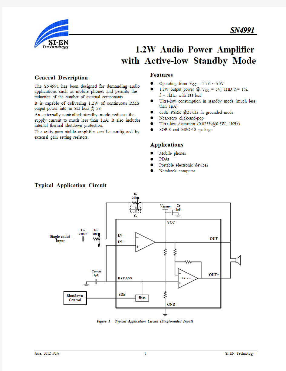
Typical Application Circuit
R F 20k
Figure 1 Typical Application Circuit (Single-ended Input)
Figure 2 Typical Application Circuit (Differential Input)
Pin Configuration
Pin Description
Pin No. Function Description
SOP MSOP IN+
1
3
Positive input of the first amplifier.
OUT- 2 5
Negative output of the SN4991. Connected to the load
and to the feedback resistor R F . IN- 3 4 Negative input of the first amplifier, receives the audio
input signal. Connected to the feedback resistor R F and
to the input resistor R IN . GND 4 7 Ground.
BYPASS 5 2
Bypass capacitor pin which provides the common mode voltage (V CC /2). OUT+
6
8
Positive output of the SN4991. Connected to the load.
SDB 7 1
The device enters shutdown mode when a low level is
applied on this pin. VCC
8
6
Positive analog supply of the chip.
Ordering Information
Order Number Package Type QTY/Reel Operating Temperature Range
SN4991ID08E SOP-8
2500 -40°C ~ +85°C SN4991IE08E MSOP-8
SN4991□□□□
Environmental Code
E: RoHS
Pin Code
08: 8 Pins
Package Type
D: SOP
E: MSOP
Temperature Code
I: Industrial, -40°C ~ +85°C
Absolute Maximum Ratings
Supply voltage, V CC --------------------------------------------------------------------------------------------------------------------- -0.3V ~ +6.0V Input voltage ----------------------------------------------------------------------------------------------------------------------- ?0.3V ~ V CC + 0.3V Maximum junction temperature, T JMAX ------------------------------------------------------------------------------------------------------- 150°C Operating temperature range, T A ---------------------------------------------------------------------------------------------------- -40°C ~ +85°C Storage temperature range, T STG ------------------------------------------------------------------------------------------------- –65°C ~ +150°C
Stresses beyond those listed under “Absolute Maximum Ratings” may cause permanent damage to the device. These are stress ratings only and functional operation of the device at these or any other condition beyond those indicated in the operational sections of the specifications is not implied. Exposure to absolute maximum rating conditions for extended periods may affect device reliability.
Electrical Characteristics V CC = 5V (Note 1 or specified)
The following specifications apply for C IN = 0.22μF, R IN = R F = 20k ?, C BYPASS = 1μF, unless otherwise specified. Limits apply for T A = 25°C. Symbol Parameter
Condition
Min. Typ. Max. Unit
I CC
Quiescent power supply current
V CC = 0V , I O = 0A, no Load 4.8 mA I SD Shutdown current V SDB = GND, R L = ∞ 1 μA
V SDB_H Shutdown voltage input high V CC = 5.5V 1.4 V V SDB_L Shutdown voltage input low V CC = 2.7V 0.4 V V OS Output offset voltage
15 mV Po
Output power (8?)
THD+N = 1%; f = 1kHz 1.18 W
THD+N = 10%; f = 1kHz
1.46
t WU Wake-up time (Note 2)
C BYPASS = 1μF 115 ms THD+N Total harmonic distortion+noise
(Note 2) Po = 0.5Wrms; f = 1kHz 0.025 % PSRR
Power supply rejection ratio (Note 2)
V Ripple p-p = 200mV Input Grounded
f = 217Hz 65 dB
f = 1kHz
77
Electrical Characteristics V CC = 3V (Note 1 or specified)
The following specifications apply for C IN = 0.22μF, R IN = R F = 20k ?, C BYPASS = 1μF, unless otherwise specified. Limits apply for T A = 25°C.
Symbol Parameter Condition Min. Typ. Max. Unit
I CC
Quiescent power supply current
V CC = 0V , Io = 0A, no Load 3.8 mA
I SDB Shutdown current V SDB = GND, R L = ∞ 1 μA
Po
Output power (8?)
THD+N = 1%; f = 1kHz 405 mW
THD+N = 10%; f = 1kHz
502
t WU Wake-up time (Note 2)
C BYPASS = 1μF 102 ms
THD+N Total harmonic distortion+noise
(Note 2)
Po = 0.3Wrms; f = 1kHz 0.027
%
Note 1: Production testing of the device is performed at 25°C. Functional operation of the device and parameters specified over other
temperature range, are guaranteed by design, characterization and process control. Note 2: Guaranteed by design.
Typical Performance Characteristic
T H D +N (%)
Output Power (W)
10m
2
20m
50m
100m 200m 500m
1
Figure 3 THD+N vs. Output Power
Frequency (Hz)
T H D +N (%)
Figure 5
THD+N vs. Frequency
Figure 7 PSRR vs. Frequency
T H D +N (%)
Output Power (W)
10m
2
20m 50m 100m 200m 500m 1
Figure 4 THD+N vs. Output Power
00
Frequency (Hz)
T H D +N (%)
Figure 6 THD+N vs. Frequency
Figure 8 PSRR vs. Frequency
Frequency (Hz)
O u t p u t N o i s e V o l t a g e (V )
1010020304050
70
5k
Figure 9 Noise Floor
Figure 10 Output Power vs. Power Supply
Application Information
BTL Configuration Principle
The SN4991 is a monolithic power amplifier with a BTL output type. BTL (bridge tied load) means that each end of the load is connected to two single-ended output amplifiers. Thus, we have:
Single-ended output 1 = V OUT+ = V OUT (V) Single ended output 2 = V OUT- = -V OUT (V) and
V OUT+ – V OUT- = 2V OUT (V) The output power is:
L
OUT OUT R V P RMS 2
)2(=
For the same power supply voltage, the output power in BTL configuration is four times higher than the output power in single ended configuration.
Gain in a Typical Application Schematic
The typical application schematic is shown in Figure 1 on page 1.
In the flat region (no C IN effect), the output voltage of the first stage is (in V olts):
IN
F
IN OUT R R V V )
(-=- For the second stage: V OUT+ = -V OUT- (V) The differential output voltage is (in V olts):
IN
F
IN
OUT OUT R R V V V 2=--+ The differential gain named gain (G V ) for more convenient usage is:
IN
F IN OUT OUT V R R
V V V G 2=-=
-+
V OUT+ is in phase with V IN and V OUT- is phased 180° with
V IN . This means that the positive terminal of the loudspeaker should be connected to V OUT+ and the negative to V OUT-.
Low and High Frequency Response
In the low frequency region, C IN starts to have an effect. C IN forms with R IN a high-pass filter with a -3dB cut-off frequency. f CL is in Hz.
IN
IN CL C R f π21=
In the high frequency region, you can limit the bandwidth by adding a capacitor (C F ) in parallel with R F . It forms a low-pass filter with a -3dB cut-off frequency.
f CH is in Hz.
F
F CH C R f π21
=
Decoupling of the Circuit
Two capacitors are needed to correctly bypass the SN4991: a power supply bypass capacitor C S and a bias voltage bypass capacitor C BYPASS .
C S has particular influence on the THD+N in the high frequency region (above 7kHz) and an indirect influence on power supply disturbances. With a value for C s of 1μF, you can expect THD+N levels similar to those shown in the datasheet.
In the high frequency region, if C S is lower than 1μF, it increases THD+N and disturbances on the power supply rail are less filtered.
On the other hand, if C S is higher than 1μF, those disturbances on the power supply rail are more filtered. C BYPASS has an influence on THD+N at lower frequencies, but its function is critical to the final result of PSRR (with input grounded and in the lower frequency region).
If C BYPASS is lower than 1μF, THD+N increases at lower frequencies and PSRR worsens.
If C BYPASS is higher than 1μF, the benefit on THD+N at lower frequencies is small, but the benefit to PSRR is substantial.
Note that C IN has a non-negligible effect on PSRR at lower frequencies. The lower the value of C IN , the higher the PSRR is.
Wake-up Time (t WU )
When the standby is released to put the device ON, the bypass capacitor C BYPASS will not be charged immediately. As C BYPASS is directly linked to the bias of the amplifier, the bias will not work properly until the C BYPASS voltage is correct. The time to reach this voltage is called wake-up time or t WU and specified in the electrical characteristics table with C BYPASS = 1μF.
Pop Performance
Pop performance is intimately linked with the size of the input capacitor C IN and the bias voltage bypass capacitor C BYPASS .
The size of C IN is dependent on the lower cut-off frequency and PSRR values requested. The size of C BYPASS is dependent on THD+N and PSRR values requested at lower frequencies.
Moreover, C BYPASS determines the speed with which the amplifier turns on.
Classification Reflow Profiles
Profile Feature
Pb-Free Assembly
Preheat & Soak
Temperature min (Tsmin) Temperature max (Tsmax) Time (Tsmin to Tsmax) (ts) 150°C 200°C 60-120 seconds Average ramp-up rate (Tsmax to Tp) 3°C/second max. Liquidous temperature (TL) Time at liquidous (tL)
217°C 60-150 seconds Peak package body temperature (Tp)* Max 260°C Time (tp)** within 5°C of the specified classification temperature (Tc) Max 30 seconds Average ramp-down rate (Tp to Tsmax) 6°C/second max. Time 25°C to peak temperature
8 minutes max.
Figure 11 Classification Profile
Tape and Reel Information
SOP-8
MSOP-8
Package Information
SOP-8
MSOP-8
Note: All dimensions in millimeters unless otherwise stated.