乘法器VERILOG
Advances in Computational Sciences and Technology
ISSN 0973-6107 Volume 3 Number 2 (2010) pp. 223–235
? Research India Publications
https://www.360docs.net/doc/cc16950438.html,/acst.htm
Run-Time Reconfigurable Pipelined Modified
Baugh-Wooley Multipliers
Aswathy Sudhakar1 and D. Gokila2
1,2VLSI Design Group, Department of Electronics and Communication Engineering Amrita School of Engineering, Amrita Vishwa Vidyapeetham,
Coimbatore-641105, India
E-mal:1achu1921@https://www.360docs.net/doc/cc16950438.html,, 2d_gokila@https://www.360docs.net/doc/cc16950438.html,
Abstract
FPGA implementation of multipliers causes area overhead problem since they are implemented separately with separate functionalities even if they are to perform the same calculation. This also causes increased power dissipation.
Also FPGA device sizes can only increase as fast as the silicon process technology will allow it to. The multiplier redundancy can be removed by Run-Time Reconfiguration which is the very best solution for reducing FPGA area thereby reducing the power consumption. In this paper, the basic structure of the Baugh-Wooley (BW) multiplier, which is proved to be the best suitable choice for multiplier reconfiguration is modified for optimizing constraints like speed, area, accuracy and power consumption. The reconfiguration on Baugh-Wooley multiplier is explained with respect to the optimum reconfiguration constraints. Various techniques like pipelining, true rounding, 2-D pipeline gating are effectively incorporated in the modified BW multiplier design to optimize the constraints. The large speed overhead caused by reconfiguration limits it from practical applications which are overcome by using pipeline registers. Effective use of pipeline registers is made so as to control the speed overhead problem occurring through the reconfiguration of multiplier functionalities. The results are compared between non-reconfigurable, non-reconfigurable pipelined and reconfigurable 8-stage pipelined modified BW multiplier architectures for n=8, 16, 32, and 64. It is obtained that the Partial Run-Time Reconfiguration reduces the area by 31-40%. Pipelining improves the speed by 4-5 times whereas run-time reconfiguration results in 2-5% reduction in overall power dissipation.
224 Aswathy Sudhakar and D. Gokila Keywords: Run-Time Reconfiguration, Baugh-Wooley Multiplier, Fixed-
Width Multiplier, Reconfiguration Speed, Sub-Word Multiplication, 2-D Pipeline Gating and Pipeline Register.
Introduction
Digital designs can be implemented on a configurable logic platform provided by FPGAs. The designs based on FPGAs are beginning to dominate in almost all fields due to various advantages like simplicity, portability, high performance and low power dissipation and as the complexity relentlessly increases, FPGAs are beginning to be used in application domains requiring intensive arithmetic operations, such as signal processing. FPGAs are now-a-days technologically evolved and complex that they are able to host an entire system-on-chip. Recent advances in VLSI technology provide very complex digital-signal-processing algorithms to be cost effectively implemented. But at the same time, the design complexity to achieve high-speed performance, reduced area and power efficiency becomes a major challenge. FPGAs are very costly in terms of area occupation and more importantly in terms of power consumption. Also a multi-million gate FPGA era is expected. Power consumption in a chip increases due to increase in the number of gates and also due to the implementation of redundant modules serving the same functionality repeatedly. It also increases the heat loss which results in device damage. A very effective solution consists of reconfiguration of FPGAs.
Reconfiguration of multipliers in an FPGA reduces the power dissipation as well as area overhead mainly by limiting the number of redundant modules. There are two levels of reconfiguration architecture [1]: design-time (static configuration of some architectural parameters) and at run-time (dynamic reconfiguration of the overall functionality or algorithm implemented by the array). Dynamic reconfiguration is heavily used to implement a given computation, and it is utilized to exploit time multiplexing of the FPGA resources and ensure software-oriented flexibility of the cells. Dynamic or run-time reconfiguration (RTR) [1] is defined as the ability to change or modify the functional configuration of a device on the fly. For practically any DSP system, multiplication is a vital function. The reconfiguration of multiplier blocks is thus taken into consideration to improve the reconfiguration constraints. The various multiplier types based on architectures [2, 3, 4], introduced necessitates the need for an efficient multiplier selection for a particular function. From the comparisons, the Baugh-Wooley Multiplier is the power and area efficient one and is the best suited choice for reconfiguration due to high-speed and regularity in the architecture. Reconfiguration of BW multipliers [5] keeping n+w most significant columns [6, 10] is performed for reducing the power dissipation. But this generates accuracy reduction in low-resolution fixed-width multiplication caused by the redundant bits in the sign-extension circuit and limits its reconfiguration efficiency. In [7], the presented work reduced the accuracy degradation in fixed-width multipliers by truncation with rounding technique which has accuracy almost equal to the rounding technique with a little circuit complexity. With the 2-D pipeline gating [8] technique in the Baugh-Wooley reconfigurable multiplier, the low-resolution errors
Run-Time Reconfigurable Pipelined Modified 225 are minimized as it improves the regularity of the computing architecture. But this has area overhead and increased redundancy and are minimized in [9] by the sub-word multiplication technique. Here the limited pipelining structures fail to achieve high speed and 2-D pipeline gating causes timing mismatch which leads to increased latency. In [11], a BW multiplier which included techniques to save the power consumption with truncated multiplication. This has poor accuracy and increased redundancy. In [12], the accuracy degrades due to variation in the co-ordination of processing of bits in the input samples. So for almost all the techniques discussed, the implementations causes the reconfiguration overhead which results in a huge decrease in speed due to increased latency and hence making reconfiguration practically difficult.
In this paper, the best suited multiplier for reconfiguration, the Baugh-Wooley multiplier architecture is modified to make it suitable for reconfiguration among three arithmetic functions. The three configuration modes (CM) include: 1) n x n fixed-width multiplier 2) two n/2 x n/2 fixed-width multipliers 3) n/2 x n/2 full-precision multiplier. The constraints taken into consideration for optimization are Power Dissipation, Area, Speed and Accuracy. Various methods like pipelining, reconfiguration, true rounding, 2-D pipelining etc are incorporated in the modified BW architecture to optimize these performance constraints and to overcome the huge reconfiguration overhead in speed. Also a comparison is made between non-reconfigurable, non-reconfigurable pipelined and reconfigurable pipelined modified BW multipliers for n=8, 16, 32, and 64.
The rest of the paper is organized as follows. The modified BW Multiplier design is explained in Section 2. Section 3 gives the design of reconfigurable modified BW multiplier with optimum constraints. In Section 4, implementation results in terms of power, area and speed and comparisons are presented. Section 5 concludes the paper. Modified Baugh Wooley (BW) Multiplier Design
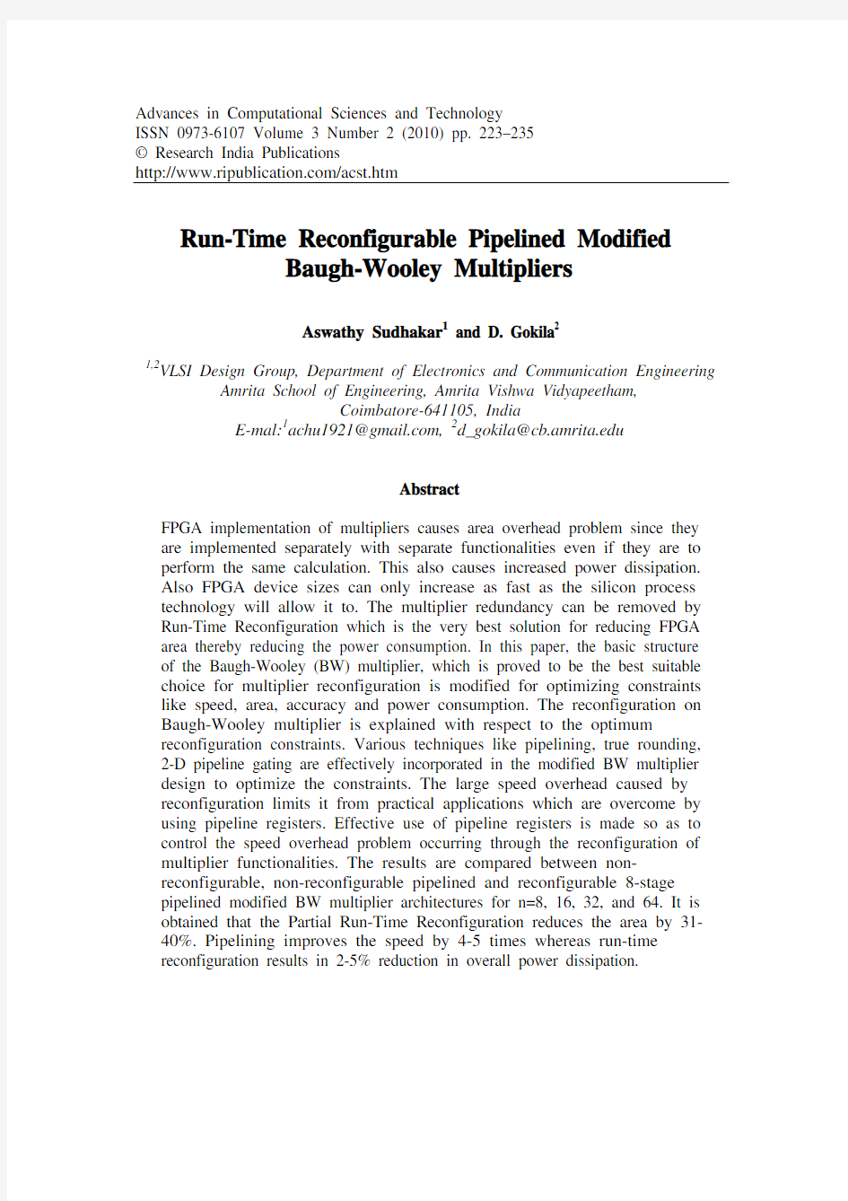
Pipelined modified BW multiplier design for n=8 is shown in Figure 1(a). The techniques added with the conventional BW multiplier are pipelining, truncation with rounding and 2-D pipelining. The pipelining effect in multiplication is shown in Figure 1(b). The registers are placed in between various multiplication stages according to the functionality required. These registers are termed as pipeline registers. The same technique is used for modifying the basic multiplier design to improve the speed. As in Figure 1(a), the partial product bits created are stored in the pipeline registers. After segregation of partial products pipeline registers follows the partial product block. This avoids the delay and the latency caused by the two’s complement calculation. When pipeline registers are used here in the design, the blocks following pipeline register access input from the register so that the preceding blocks can operate on successive data. This considerably improves the processing time of a large amount of successive input data. Pipelining ensures the partial product bits to be ready for summation simultaneously so that the errors due to latency can be removed. Latency causes the error to be propagated to the next stages of calculations. Pipelined registers are used to decrease the delay, thereby improving the speed. Here
226 Aswathy Sudhakar and D. Gokila the multiplier module itself is pipelined along with the pipelined reconfigurable structure.
True rounding or Truncation with Rounding of the partial products [8] improves the accuracy of the final output also with reduced power dissipation. True Rounding requires adding a ‘1’ at the n th least significant bit position of the product which helps to control the possible errors while truncation is performed. After segregation, the negative partial products are inverted and added to the positive partial products. The inversion is done by 2-D pipelining [7] to maintain the regularity in the design. The addition of partial products thus formed gives the final product. This design has considerable increase in speed due to pipelining and accuracy improvement due to true rounding.
(a) (b) Figure 1. (a)Efficient fixed-width modified BW multiplier for n=8; (b) Pipelining in Multiplication.
Design of Reconfigurable Modified BW Multiplier for Optimum Constraints
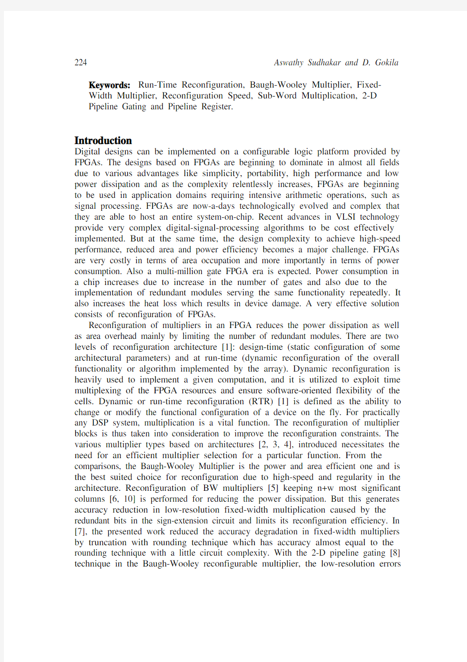
The performance constraints taken into consideration here are: 1) Power Dissipation, 2) Area, and 3) Speed. The partial product array diagram for an nxn modified BW multiplier is shown in Figure 2. Figure 2(a) shows the generalized product diagram and 2(b) shows that for n=8. Figure 2(c) shows the partial products remaining after truncation for design. Here the LSBs are masked by truncation. The ‘w’ bit decides the length of the output product. In this design ‘w=1’ is taken.
Run-Time Reconfigurable Pipelined Modified 227
(a)
(b) (c)
Figure 2: (a) Partial Product Array Diagram for an n-bit modified BW Multiplier, (b) Partial Product Array Diagram for an 8-bit modified BW Multiplier and (c) Partial products after truncation.
Figure 3: Design of reconfigurable modules (MUL1, MUL2 and MUL3).
The modules are defined by the sub-word multiplication technique [6] as shown in Figure 4. Here X [x7 x6 ……x0] and Y [y7 y6 ……y0 ] are the two 8-bit inputs. The sub-words are X1[x7 x6 x5 x4] , X0[x3 x2 x1 x0], Y1[y7 y6 y5 y4] and Y0[x3 x2 x1 x0]. It is clear from the design that MUL1 and MUL2 modules perform the fixed-width 4x4 multiplication and MUL module performs the full-precision 4x4 multiplication. This can be used for the reconfiguration between the functionalities.
228 Aswathy Sudhakar and D. Gokila
Figure 4: Sub-word multiplication (a) two n/2xn/2 multiplications (b) two n/2xn/2 partial-product array distribution.
CM1: nxn fixed-width multiplier
For an nxn multiplier, all the three reconfiguration modules are required and is shown in Figure 5(a). CM1 is taken as the prototype structure for reconfiguration after removal of LSBs as in Figure 5(b). Various configuration parameters (CP0, CP1, and CP2) are given with the reconfiguration modules so as to get the complete reconfiguration functionalities. These parameters combine with other settings to generate the corresponding functionalities. In CM1, CP0 and CP1 are set to ‘1’ and CP2 is set to ‘0’ as shown in Figure 5(c).
(a) (b) (c)
Figure 5. (a) CM1 array diagram, (b) Prototype Structure (c) Configuration parameter settings for CM1.
CM2: two n/2 x n/2 fixed-width multipliers
Configuration mode plays a role of performing two n/2 x n/2 fixed-width multiplications. In this, two copies of hardware resources are required to implement
Run-Time Reconfigurable Pipelined Modified 229 CM2. As described earlier, both MUL1 and MUL2 perform the n/2 x n/2 fixed-width multiplications and can be used. Here X1Y0 and X0Y1 are the n/2 –bit multiplications performed as shown in Figure 6(a). The configuration parameters CP0 and CP1 are set to ‘0’ and CP2 is set to ‘1’ as shown in Figure 6(b).
(a) (b)
Figure 6: (a) CM2 array diagram (b) Configuration parameter settings for CM2. CM3: n/2 x n/2 full-precision multiplier
With the minimum number of modules and partial product settings as the parameters, it is clear that MUL3 is the best suited for n/2 x n/2 full-precision multiplication. Figure 7(a) shows MUL3 as n/2 x n/2 full-precision multiplier and Figure 7(b) shows the corresponding configuration parameter settings where CP3 and CP4 are set to 1 and 0 respectively.
(a) (b)
Figure 7: (a) CM3 array diagram (b) Configuration parameter settings for CM3.
The proposed pipelined reconfigurable modified BW multiplier for n=8 is shown in Figure 8(d). According to the reconfiguration parameters required, reconfiguration modules are selected with the help of a decoder and the corresponding functionality is mapped on to the prototype structure. Here MUX and ADD in Figure 8(d) represent multiplexers and adders respectively. The MUL1 and MUL2 are required for both
230 Aswathy Sudhakar and D. Gokila CM1 and CM2 functionalities and so this is represented by t [2]. MUL3 is represented by t [1:0] and needed for CM1 and CM3. A decoder circuit is used to decode these select bit values. As shown in the figure, t [2] is the select bit for first MUX and t[3] is the select bit for the second MUX. The system works as: during CM1; all the three multiplier modules are required as shown in the Figure 8(c). The corresponding decoder values shows that t [3] is set to ‘1’ and t[2] is set to ‘0’ as in Figure 8(b). Hence the first MUX produces MUL3 as output. ADD1 adds the MUL1 and MUL2 outputs. Both these results are then added in ADD2. The second multiplexer selects this as the output since the select bit t [3]= ‘1’. This gives the n-bit fixed-width multiplication output (CM1). During CM2, first MUX produces the concatenated output from MUL1 and MUL2. The second MUX selects this as the output since the select bit t [3] = ‘0’. Thus two n/2-bit fixed-width multiplications can be performed by CM2. During CM3, t [3] and t [2] are 0 and MUL3 output is directly transferred to the output giving n/2 x n/2 full-precision multiplication. The pipeline registers serves the basic functionality of improving the speed by processing successive data without latency. Here 8-stage pipelining is incorporated in this design. Thus reconfiguration makes the architecture power-efficient and area-efficient where as pipelining improves the speed. The true rounding and 2-D pipelining is also incorporated in the above design practically to improve the accuracy though it is not shown.
(d)
Figure 8: (a) Configuration Parameters, (b) Truth Table of Decoder, (c) Configuration Parameter Settings, and (d) Proposed Pipelined Reconfigurable Modified BW Multiplier Architecture.
Run-Time Reconfigurable Pipelined Modified 231 Implementation Results and Comparisons
The implementation is done in Verilog HDL and logic simulation is done in ModelSim Simulator 6.2 and the synthesis is done using Altera Quartus II 7.2. The comparison between various multiplier architectures (4-bit) differentiated according to the architecture is shown in Table 1. From Table 1(a) and 1(b) it is clear that the Baugh-Wooley multiplier architecture is the best suited for reconfiguration of FPGAs. Also it is clear that the pipelining stages as in Figure 9 improve the speed by 6% with negligible increase in power in 4-bit Baugh-Wooley multiplier architecture. So in order to reduce the reconfiguration overhead in speed, pipelining can be used to improve the speed. Also reconfiguration in pipelined multipliers reduces the area overhead due to pipeline registers.
Table 1(a). Area, Speed, and Power Dissipation for various non-pipelined multiplier architectures (4-bit).
Multiplier Architecture Number
of LUTs
Clock-Period
(ns)
Speed (MHz) Power Dissipation
(mW)
Wallace Tree 34 15.852 63.08 68.52
Booth 42 16.318 61.28 67.98
Baugh-
Wooley
28 15.861 63.03 67.84
Table 1(b). Area, Speed, and Power Dissipation for various pipelined multiplier architectures (4-bit).
Multiplier Architecture Number
of LUTs
Clock-Period
(ns)
Speed (MHz) Power Dissipation
(mW)
Wallace Tree 56 15.026 66.55 68.82
Booth 60 16.012 62.45 68.16
Baugh-Wooley 32 15.029 66.53 67.97
Figure 9: Speed Comparison between various pipelined and non-pipelined multiplier architectures (4-bit).
232 Aswathy Sudhakar and D. Gokila The synthesis results of non-reconfigurable modified BW multiplier, reconfigurable modified BW multiplier, and non-reconfigurable pipelined and pipelined reconfigurable modified BW multipliers are shown in Table 2 and Table 3. From Table 2(a), it is clear that pipelining improves the speed of a non-reconfigurable modified BW multiplier by 4-5 times for various values of n whereas considerable area overhead caused by pipelining is reduced by reconfiguring the architecture. From Table 2 it is clear that for ‘n’ value greater than 32 the design is optimized.
Table 2(a): Area and Speed comparison between Non-Reconfigurable and Reconfigurable Modified BW Multiplier.
Table 2(b): Area and Speed comparison between Non-Reconfigurable Pipelined and Pipelined Reconfigurable Modified BW Multiplier.
Run-Time Reconfigurable Pipelined Modified 233 By making the system reconfigurable we can reduce the area overhead problem as shown in Table 2(a). Area reduces to 31-40 % with only a slight degradation in speed (2-6 %) caused by reconfiguration time overhead which is negligible when compared to the added advantages of pipelining. As a result the pipelining and reconfiguration together gives an improvement of 18-28 % improvement in speed when compared with non-reconfigurable non-pipelined architecture.
From Table 2(a) and 2(b), it is clear that as the number of bits increases the area can be optimized. So the design is well suited for higher input bits. Table 3 shows the power dissipation comparison between various non-reconfigurable, non-reconfigurable pipelined and reconfigurable pipelined architectures for n=8, 16, 32, and 64. In general from table 3(a), it is seen that the reconfiguration produces a reduction in power by 2-11 % in non-pipelined structures whereas the reconfiguration in the pipelined structure improves the power dissipation by 2-5 % as shown in table 3(b). Hence the overall power dissipation decreases after pipelining and reconfiguration by about 2-5%. Here also it is clear from Table 3(a) and 3(b) that as the value of ‘n’ increases the power dissipation can be compared for pipelined and non-pipelined structures and the design becomes power optimized. From the results it is clear that pipelining increases the speed by 6% in a 4-bit Baugh-Wooley multiplier and the optimization of constraints with pipelining and reconfiguration gives about 2-5% reduction in power dissipation, 4-5 times increase in speed and area reduces by 31-40% by reconfiguration. Thus the large speed overhead due to reconfiguration is controlled with the effective use of pipelining.
Table 3(a): Power Dissipation Comparison between Non-Reconfigurable and Reconfigurable Modified BW Multiplier.
234 Aswathy Sudhakar and D. Gokila Table 3(b): Power Dissipation Comparison between Non-Reconfigurable Pipelined and Pipelined Reconfigurable BW Multiplier.
Conclusion
In this paper the BW multiplier architecture has been modified and Dynamic Reconfiguration has been implemented for optimizing the reconfiguration constraints like speed, area, accuracy and power consumption. Various techniques like pipelining, true rounding, 2-D pipeline gating have been effectively incorporated in the modified BW multiplier design to optimize the constraints. Pipelined registers have been used to overcome the large speed overhead caused by reconfiguration limits it from practical applications. An improvement in speed is shown with the modification of basic Baugh-Wooley multiplier architecture making it suitable for reconfiguration. Comparisons are done between the results obtained for non-reconfigurable, non-reconfigurable pipelined and pipelined reconfigurable modified BW multiplier architectures for n=8, 16, 32, and 64. Pipelining improves the speed by 4-5 times whereas run-time reconfiguration results in 2-5% reduction in overall power dissipation. Area reduces to 31-40% in pipelined reconfigurable architecture when compared to the non-reconfigurable pipelined architectures.
References
[1][White Paper] “ALTERA: FPGA run-time reconfiguration two approaches”.
[2]Sadiq M. Sait, Aamir A. Farooqui and Gerhard. F. Beckhoff; “A Novel
Technique for Fast Multiplication” IEEE International Conference on computers and Communications on March 1995.
[3] A. Habibi and P. A. Wintz, "Fast multipliers," IEEE Trans. Comput., vol. C-
19, pp. 153-157, Feb. 1970.
[4]R. GNANASEKARAN; “A Fast Serial-Parallel Binary Multiplier”; IEEE
Transactions On Computers, Vol. C-34, No. 8, August 1985C. R. Baugh and
Run-Time Reconfigurable Pipelined Modified 235
B. A. Wooley, “A two’s complement parallel array multiplication algorithm,”
IEEE Trans. Compt., vol. C-22, no. 12, pp.1045-1047, Dec. 1973.
[5] C. R. Baugh and B. A. Wooley, “A two’s complement parallel array
multiplication algorithm,” IEEE Trans. Compt., vol. C-22, no. 12, pp.1045-
1047, Dec. 1973.
[6]Schulte, M.J., Stine, J.E., and Jansen, J.G.: ‘Reduced power dissipation
through truncated multiplication’. Proc. IEEE Alessandro Volta Memorial Workshop on Low-Power Design, 1999, pp. 61 2 69.
[7] E.E.Swartzlander, Jr., “Truncated multiplication with approximate rounding,”
in Proc. 33rd Asilomar Conference on Signals, Systems, and Computers, 1999,
vol. 2, pp. 1480-1483.
[8]J. Di and J. S. Yuan, “Run-time reconfigurable power-aware pipelined signed
array multiplier design,” in Proc. IEEE International Symposium on Signals, Circuits, and Systems, July 2003, vol. 2, pp. 405-406.
[9]S. Krithivasan, M. J. Schulte, and J. Glossner, “A sub word-parallel
multiplication and sum- of-squares unit,” IEEE Comp. society Annual Symposium on VLSI, pp. 273-274, Feb. 2004.
[10]L. D. Van and C. C. Yang, “Generalized low-error area-efficient fixed-width
multipliers,” IEEE Trans. Circuits Syst. I, vol. 52, pp. 1608-1619, Aug. 2005 [11]S.R.Kuang and J.P.Wang , “Design of power-efficient pipelined truncated
multipliers with various output precision”, IET Computers and Digital Techniques,vol.1,pp.129-136,Mar.2007.
[12]Tu, J Van, L ,“ Power-Efficient Pipelined Reconfigurable Fixed-Width Baugh-
Wooley Multipliers” ,IEEE Transactions on Computers : vol.58,pp.1346-1355,
Oct. 2009.
Verilog各种倍分频器设计
module odd_division(clk,rst,count,clk_odd); /*count没必要放在端口中,这里只是为了仿真时观察*/ input clk,rst; output clk_odd; output[3:0] count; reg clk_odd; reg[3:0] count; parameter N = 6; /*6分频* / always @ (posedge clk) if(! rst) begin count <= 1'b0; clk_odd <= 1'b0; end else if ( count < N/2-1) begin count <= count + 1'b1; end else begin count <= 1'b0; clk_odd <= ~clk_odd; end endmodule 奇数倍分频:归类为一般的方法为:对于实现占空比为50%的N倍奇数分频,首先进行上升沿触发进行模N计数,计数从零开始,到N-1)/2进行输出时钟翻转,然后经过(N+1)/2再次进行翻转得到一个占空比非50%奇数n分频时钟。再者同时进行下降沿触发的模N计数,到和上升沿过(N-1)/2时,输出时钟再次翻转生成占空比非50%的奇数n分频时钟。两个占空比非50%的n分频时钟相或运算,得到占空比为50%的奇数n分频时钟。 module even_division(clk,rst,count1,count2,clk_even); /*count1,count2没必要放在端口中,这
里只是为了仿真时观察*/ input clk,rst; output[3:0] count1,count2; output clk_even; reg[3:0] count1,count2; reg clkA,clkB; wire clk_even,clk_re; parameter N = 5; /*5分频*/ assign clk_re = ~clk; assign clk_even = clkA | clkB; always @(posedge clk) if(! rst) begin count1 <= 1'b0; clkA <= 1'b0; end else if(count1 < (N - 1)) begin count1 <= count1 + 1'b1; /*这里是非阻塞赋值是先执行了下面的IF判断,最后才赋的值。最初看这程序时没注意,想了好半天*/ if(count1 == (N - 1)/2) begin clkA <= ~clkA; end end else begin clkA <= ~clkA;
用Verilog语言实现任意整数分频器
用Verilog语言实现任意整数分频器 分频器是FPGA设计中使用频率非常高的基本设计之一,尽管在目前大部分设计中,广泛使用芯片厂家集成的锁相环资源,如赛灵思(Xilinx)的DLL.来进行时钟的分频,倍频以及相移。但是对于时钟要求不高的基本设计,通过语言进行时钟的分频相移仍然非常流行,首先这种方法可以节省芯片内部的锁相环资源,再者,消耗不多的逻辑单元就可以达到对时钟操作的目的。另一方面,通过语言设计进行时钟分频,可以看出设计者对设计语言的理解程度。因此很多招聘单位在招聘时往往要求应聘者写一个分频器(比如奇数分频)以考核应聘人员的设计水平和理解程度。下面讲讲对各种分频系数进行分频的方法:第一,偶数倍分频:偶数倍分频应该是大家都比较熟悉的分频,通过计数器计数是完全可以实现的。如进行N倍偶数分频,那么可以通过由待分频的时钟触发计数器计数,当计数器从0计数到N/2-1时,输出时钟进行翻转,并给计数器一个复位信号,使得下一个时钟从零开始计数。以此循环下去。这种方法可以实现任意的偶数分频。电路上只需一个D触发器和一个非门即可实现,Q(n+1)=D,D=~Q(n),clk_out=Q(n+1) . 第二,奇数倍分频:奇数倍分频常常在论坛上有人问起,实际上,奇数倍分频有两种实现方法: 占空比为非50%的三分频时钟,完全可以通过计数器来实现,如进行三分频,通过待分频时钟上升沿触发计数器进行模三计数,当计数器计数到邻近值进行两次翻转,比如可以在计数器计数到1时,输出时钟进行翻转,计数到2时再次进行翻转。即是在计数值在邻近的1和2进行了两次翻转。这样实现的三分频占空比为1/3或者2/3。 module three(clk_in,rst,clk_out); // 三倍频 inputclk_in,rst; output clk_out; reg clk_out; reg [1:0] count; always @(negedgerst or posedgeclk_in) begin if(rst==0) begin count<=0; clk_out<=0; end else begin count<=count+1; if(count==1) clk_out<=~clk_out; else if(count==2) begin clk_out=~clk_out; count<=0; end end end endmodule 仿真图 另一种实现: module div3(CLKIN,CLKOUT,RESETn); //依然是三倍频 inputCLKIN,RESETn;
实验六--Verilog设计分频器计数器电路答案
实验六 Verilog设计分频器/计数器电路 一、实验目的 1、进一步掌握最基本时序电路的实现方法; 2、学习分频器/计数器时序电路程序的编写方法; 3、进一步学习同步和异步时序电路程序的编写方法。 二、实验内容 1、用Verilog设计一个10分频的分频器,要求输入为clock(上升沿有效),reset(低电平复位),输出clockout为4个clock周期的低电平,4个clock周期的高电平),文件命名为fenpinqi10.v。 2、用Verilog设计一异步清零的十进制加法计数器,要求输入为时钟端CLK(上升沿)和异步清除端CLR(高电平复位),输出为进位端C和4位计数输出端Q,文件命名为couter10.v。 3、用Verilog设计8位同步二进制加减法计数器,输入为时钟端CLK(上升沿有效)和异步清除端CLR(低电平有效),加减控制端UPDOWN,当UPDOWN为1时执行加法计数,为0时执行减法计数;输出为进位端C和8位计数输出端Q,文件命名为couter8.v。 4、用VERILOG设计一可变模数计数器,设计要求:令输入信号M1和M0控制计数模,当M1M0=00时为模18加法计数器;M1M0=01时为模4加法计数器;当M1M0=10时为模12加法计数器;M1M0=11时为模6加法计数器,输入clk上升沿有效,文件命名为mcout5.v。 5、VerilogHDL设计有时钟时能的两位十进制计数器,有时钟使能的两位十进制计数器的元件符号如图所示,CLK是时钟输入端,上升沿有效;ENA是时钟使能控制输入端,高电平有效,当ENA=1时,时钟CLK才能输入;CLR是复位输入端,高电平有效,异步清零;Q[3..0]是计数器低4位状态输出端,Q[7..0]是高4位状态输出端;COUT是进位输出端。 三、实验步骤 实验一:分频器 1、建立工程
verilogHDL分频器(奇数分频和偶数分频)
module clk_div( //-----------input----------- iCLK, div, //-----------output---------- oCLK ); //-----------input----------- parameter WIDE=14; input iCLK; input[WIDE-1:0]div; //-----------output----------- output oCLK; wire oCLK_odd; wire oCLK_even; assign oCLK=div[0]?oCLK_odd:oCLK_even; div_odd DUTo (.iCLK(iCLK),.oCLK(oCLK_odd),.div(div)); div_even DUTe (.iCLK(iCLK),.oCLK(oCLK_even),.div(div)); endmodule // odd module div_odd( //--------input-------- iCLK, div, //--------output-------- oCLK ); //--------input-------- parameter WIDE=14; input iCLK; input[WIDE-1:0]div; //--------output-------- output oCLK; reg outCLK;
/* =========================== solve 1 =========================== reg cout; reg[WIDE-1:0] cnt; initial cnt=0; wire inCLK; reg cc; initial cc=0; always @(posedge cout) cc<=~cc; assign inCLK = iCLK^cc; always @(posedge inCLK) begin if(cnt<(div[WIDE-1:1])) begin cnt<=cnt+1; cout<=1'b0; end else begin cnt<=0; cout<=1'b1; end end always @(negedge iCLK) outCLK <= cout; assign oCLK=cc; */ //======================== //solve 2 //======================== reg[WIDE-1:0] cnt_a; initial cnt_a=0; reg[WIDE-1:0] cnt_b; initial cnt_b=0; reg cout_a;
分频器的verilog hdl语言
分频器的verilog HDL描述(转) 分频器,在许多涉及时序的电路设计中都会用到,在这里,我转载某位高人的文章,关于分频器的设计 偶数倍分频:偶数倍分频应该是大家都比较熟悉的分频,通过计数器计数是完全可以实现的。如进行N倍偶数分频,那么可以通过由待分频的时钟触发计数器计数,当计数器从0计数到N/2-1时,输出时钟进行翻转,并给计数器一个复位信号,使得下一个时钟从零开始计数。以此循环下去。这种方法可以实现任意的偶数分频。 module odd_division(clk,rst,count,clk_odd); input clk,rst; output clk_odd; output[3:0] count; reg clk_odd; reg[3:0] count; parameter N = 6; always @ (posedge clk) if(! rst) begin count <= 1'b0; clk_odd <= 1'b0; end else if ( count < N/2-1) begin count <= count + 1'b1; end else begin
clk_odd <= ~clk_odd; end endmodule 奇数倍分频:归类为一般的方法为:对于实现占空比为50%的N倍奇数分频,首先进行上升沿触发进行模N计数,计数从零开始,到(N-1)/2进行输出时钟翻转,然后经过(N-1)/2再次进行翻转得到一个占空比非50%奇数n分频时钟。再者同时进行下降沿触发的模N 计数,到和上升沿过(N-1)/2时,输出时钟再次翻转生成占空比非50%的奇数n分频时钟。两个占空比非50%的n分频时钟相或运算,得到占空比为50%的奇数n分频时钟。 module even_division(clk,rst,count1,count2,clk_even); input clk,rst; output[3:0] count1,count2; output clk_even; reg[3:0] count1,count2; reg clkA,clkB; wire clk_even; parameter N = 5; assign clk_re = ~clk; assign clk_even = clkA | clkB; always @(posedge clk) if(! rst) begin count1 <= 1'b0; clkA <= 1'b0; end else
任意分频Verilog实现
1. 偶数倍(2N)分频 使用一模N计数器模块即可实现,即每当模N计数器上升沿从0开始计数至N-1时,输出时钟进行翻转, 同时给计数器一复位信号使之从0开始重新计数,以此循环即可。偶数倍分频原理示意图见图1。 2. 奇数倍(2N+1)分频 (1)占空比为X/(2N+1)或(2N+1-X)/(2N+1)分频,用模(2N+1)计数器模块可以实现。取0至2N-1之间一数值X(0,当计数器时钟上升沿从0开始计数到X值时输出时钟翻转一次,在计数器继续计数达到2N 时,输出时钟再次翻转并对计数器置一复位信号,使之从0开始重新计数,即可实现。 (2)占空比为50%的分频,设计思想如下:基于(1)中占空比为非50%的输出时钟在输入时钟的上升沿 触发翻转;若在同一个输入时钟周期内,此计数器的两次输出时钟翻转分别在与(1)中对应的下降沿触发翻转,输出的时钟与(1)中输出的时钟进行逻辑或,即可得到占空比为50%的奇数倍分频时钟。当然其 输出端再与偶数倍分频器串接则可以实现偶数倍分频。奇数倍分频原理示意图见图2。(这也是许多公司常出的面试题,^_^,是不是很简单?) 3. N-0.5倍分频 采用模N计数器可以实现。具体如下:计数器从0开始上升沿计数,计数达到N-1上升沿时,输出时钟需翻转,由于分频值为N-0.5,所以在时钟翻转后经历0.5个周期时,计数器输出时钟必须进行再次翻转,即当 CLK为下降沿时计数器的输入端应为上升沿脉冲,使计数器计数达到N而复位为0重新开始计数同时输出时钟翻转。这个过程所要做的就是对CLK进行适当的变换,使之送给计数器的触发时钟每经历N-0.5个周期就翻转一次。N-0.5倍:取N=3,分频原理示意图见图3。 对于任意的N+A/B倍分频(N、A、B∈Z,A≦B) 分别设计一个分频值为N和分频值N+1的整数分频器,采用脉冲计数来控制单位时间内两个分频器出现 的次数,从而获得所需要的小数分频值。可以采取如下方法来计算个子出现的频率: 设N出现的频率为a,则N×a+(N+1)×(B-a)=N×B+A 求解a=B-A; 所以N+1出现的频率为 A.例如实现7+2/5分频,取a为3,即7×3+8×2就可以实现。但是由于这种小数分频输出的时钟脉冲抖动很大, 现实中很少使用。 通常实现偶数的分频比较容易,以十分频为例: always @( posedge clk or posedge reset) if(reset) begin k<=0; clk_10<=0; end else if(k==4) begin k<=0;
实验六Verilog设计分频器计数器电路答案
实验六V e r i l o g设计分频器/计数器电路 一、实验目的 1、进一步掌握最基本时序电路的实现方法; 2、学习分频器/计数器时序电路程序的编写方法; 3、进一步学习同步和异步时序电路程序的编写方法。 二、实验内容 1、用Verilog设计一个10分频的分频器,要求输入为clock(上升沿有效),reset(低电平复位),输出clockout为4个clock周期的低电平,4个clock 周期的高电平),文件命名为。 2、用Verilog设计一异步清零的十进制加法计数器,要求输入为时钟端CLK (上升沿)和异步清除端CLR(高电平复位),输出为进位端C和4位计数输出端Q,文件命名为。 3、用Verilog设计8位同步二进制加减法计数器,输入为时钟端CLK(上升沿有效)和异步清除端CLR(低电平有效),加减控制端UPDOWN,当UPDOWN 为1时执行加法计数,为0时执行减法计数;输出为进位端C和8位计数输出端Q,文件命名为。 4、用VERILOG设计一可变模数计数器,设计要求:令输入信号M1和M0控制计数模,当M1M0=00时为模18加法计数器;M1M0=01时为模4加法计数器;当M1M0=10时为模12加法计数器;M1M0=11时为模6加法计数器,输入clk 上升沿有效,文件命名为。 5、VerilogHDL设计有时钟时能的两位十进制计数器,有时钟使能的两位十进制计数器的元件符号如图所示,CLK是时钟输入端,上升沿有效;ENA是
时钟使能控制输入端,高电平有效,当ENA=1时,时钟CLK才能输入;CLR 是复位输入端,高电平有效,异步清零;Q[3..0]是计数器低4位状态输出端,Q[7..0]是高4位状态输出端;COUT是进位输出端。 三、实验步骤 实验一:分频器 1、建立工程 2、创建Verilog HDL文件 3、输入10分频器程序代码并保存 4、进行综合编译 5、新建波形文件 6、导入引脚 7、设置信号源并保存 8、生成网表 9、功能仿真 10、仿真结果分析 由仿真结果可以看出clockout输出5个clock周期的低电平和5个clock 的高电平达到10分频的效果,设计正确。 实验二:十进制加法计数器(异步清零) 1、建立工程 2、创建Verilog HDL文件 3、输入加法计数器代码并保存 4、进行综合编译 5、新建波形文件 6、导入引脚 7、设置信号源并保存 8、生成网表 9、功能仿真 10、仿真结果分析
Verilog分频器设计
Verilog分频器设计 module adder(clk,z); output z; reg q; reg z; always@(posedge clk) begin if(q%9==0) z<=q; else q=q+1; end endmodule module counter9(clk,datein,z); output z; input clk; input datein; reg z; reg[3:0] q; always@(posedge clk) begin q<=q+1; if (q==4'b1001) begin q<=4'b0000; z<=datein; end end endmodule
2008-11-04 19:58 分频器是FPGA设计中使用频率非常高的基本单元之一。尽管目前在大部分设计中还广泛使用集成锁相环(如altera的PLL,Xilinx的DLL)来进行时钟的分频、倍频以及相移设计,但是,对于时钟要求不太严格的设计,通过自主设计进行时钟分频的实现方法仍然非常流行。首先这种方法可以节省锁相环资源,再者,这种方式只消耗不多的逻辑单元就可以达到对时钟操作的目的。偶数倍分频:偶数倍分频应该是大家都比较熟悉的分频,通过计数器计数是完全可以实现的。如进行N倍偶数分频,那么可以通过由待分频的时钟触发计数器计数,当计数器从0计数到N/2-1时,输出时钟进行翻转,并给计数器一个复位信号,使得下一个时钟从零开始计数。以此循环下去。这种方法可以实现任意的偶数分频。 module odd_division(clk,rst,count,clk_odd); /*count没必要放在端口中,这里只是为了仿真时观察*/ input clk,rst; output clk_odd; output[3:0] count; reg clk_odd; reg[3:0] count; parameter N = 6; /*6分频* / always @ (posedge clk) if(! rst) begin count <= 1'b0; clk_odd <= 1'b0; end else if ( count < N/2-1) begin count <= count + 1'b1; end else begin count <= 1'b0; clk_odd <= ~clk_odd;
用verilog实现任意倍分频器的方法
用verilog语言写的任意整数的分频器 占空比:对于一串理想的脉冲序列中(如方波),正脉冲的持续时间与脉冲总周期的比值,叫做这个方波的占空比。 分频分为奇分频和偶分频 第一,偶数倍分频:偶数倍分频应该是大家都比较熟悉的分频,通过计数器计数是完全可以实现的。如进行N倍偶数分频,那么可以通过由待分频的时钟触发计数器计数,当计数器从0计数到N/2-1时,输出时钟进行翻转,并给计数器一个复位信号,使得下一个时钟从零开始计数。以此循环下去。这种方法可以实现任意的偶数分频。 第二:奇数倍分频:奇数倍分频常常在论坛上有人问起,实际上,奇数倍分频有两种实现方法:首先,完全可以通过计数器来实现,如进行三分频,通过待分频时钟上升沿触发计数器进行模三计数,当计数器计数到邻近值进行两次翻转,比如可以在计数器计数到1时,输出时钟进行翻转,计数到2时再次进行翻转。即是在计数值在邻近的1和2进行了两次翻转。这样实现的三分频占空比为1/3或者2/3。如果要实现占空比为50%的三分频时钟,可以通过待分频时钟下降沿触发计数,和上升沿同样的方法计数进行三分频,然后下降沿产生的三分频时钟和上升沿产生的时钟进行相或运算,即可得到占空比为50%的三分频时钟。这种方法可以实现任意的奇数分频。归类为一般的方法为:对于实现占空比为50%的N倍奇数分频,首先进行上升沿触发进行模N计数,计数选定到某一个值进行输出时钟翻转,然后经过(N-1)/2再次进行翻转得到一个占空比非50%奇数n分频时钟。再者同时进行下降沿触发的模N计数,到和上升沿触发输出时钟翻转选定值相同值时,进行输出时钟时钟翻转,同样经过(N-1)/2时,输出时钟再次翻转生成占空比非50%的奇数n分频时钟。两个占空比非50%的n分频时钟相或运算,得到占空比为50%的奇数n分频时钟。另外一种方法:对进行奇数倍n分频时钟,首先进行n/2分频(带小数,即等于(n-1)/2+0.5),然后再进行二分频得到。得到占空比为50%的奇数倍分频。 下面讲讲进行小数分频的设计方法: 第三,小数分频:首先讲讲如何进行n+0.5分频,这种分频需要对输入时钟进行操作。基本的设计思想:对于进行n+0.5分频,首先进行模n的计数,在计数到n-1时,输出时钟赋为‘1’,回到计数0时,又赋为0,因此,可以知道,当计数值为n-1时,输出时钟才为1,因此,只要保持计数值n-1为半个输入时钟周期,即实现了n+0.5分频时钟,因此保持n-1为半个时钟周期即是一个难点。从中可以发现,因为计数器是通过时钟上升沿计数,因此可以在计数为n- 1时对计数触发时钟进行翻转,那么时钟的下降沿变成了上升沿。即在计数值为n-1期间的时钟下降沿变成了上升沿,则计数值n-1只保持了半个时钟周期,由于时钟翻转下降沿变成上升沿,因此计数值变为0。因此,每产生一个n+0.5分频时钟的周期,触发时钟都是要翻转一次。设计思路如下:
Verilog程序代码集
1.全加器 Sum=A⊕B⊕Cin Count=AB+Cin(A+B) ①数据流 module adder(a,b,Cin,Sum,Count); input [2:0]a,b; input Cin; output [2:0] Sum; output Count; assign {Count,Sum}=a+b+Cin; endmodule ②行为描述always语句 module adder(a,b,c,Cin,Sum,Count); input [4:0] a,b; input Cin; output reg [4:0] Sum; output reg Count; reg T1,T2,T3; always@(a or b or Cin) begin Sum=a^b^Cin; T1=A&B; T2=Cin&A; T3=Cin&B; Count=T1|T2|T3; end endmodule ③结构体 module adder (a,b,Cin,Sum,Count);input a,b,Cin; output Sum,Count; Xor a1(s1,a1,b); Xor a2(Sum,s1,Cin); and a3(T1,a,b); or a4(T2,a,b); and a5(T3,Cin,T2); or a6(Count,T1,T3); Endmodule 2.数值比较器 ①判断两值是否相等 module compare(a,b,equal); input [7:0] a,b; output equal; assign equal=(a==b)?|0; ②谁大谁输出 module compare(a,b,out); input [7:0] a,b; output reg[7:0] out; always@(a or b) begin if (a>b) out<=a; else if (a==b) out<=a; else out<=b; end endmodule ③输出参数 module compare(a.b.xgy,xsy,xey); input [7:0] x,y; output reg xgy,xsy,xey; always@(x or y) begin if (x==y) xey=1; else xey=0; if (x>y) begin xgy=1;xsy=0;end else if (x 四分频 module quarter_clk(reset,clk_in,clk_out); input clk_in,reset; output clk_out; reg clk_out; reg [4:0]count; always@(posedge clk_in) begin if(!reset) clk_out=0; else if (count<1) begin count<=count+1; end else begin count<=0; clk_out=~clk_out; end end endmodule 仿真 `define clk_cycle 50 module test_quarter_clk; reg clk,reset; wire clk_out; always #`clk_cycle clk=~clk; initial begin clk=0; reset=1; #100 reset=0; #100 reset=1; #10000 $stop; end quarter_clk quarter_clk1(reset,clk,clk_out); endmodule 7分频 module div7(rst,clk,cout1,cout2,cout); input clk,rst; output cout1,cout2,cout; reg [2:0] m,n; wire cout; reg cout1,cout2; assign cout=cout1|cout2; always @(posedge clk) begin if(rst) begin cout1<=0;m<=0;end else if(!rst) begin if(m==6) begin m<=0;end else m<=m+1; if(m==2) cout1=~cout1; else if(m==5) c out1=~cout1; end end always @(negedge clk) begin if(rst) begin cout2<=0;n<=0;end else if(!rst) begin if(n==6) begin n<=0;end else n<=n+1; if(n==2) cout2=~cout2; else if(n==5) cout2=~cout2; end end Endmodule 仿真 `timescale 1ns / 1ps `define clk_cycle 50 module qii; reg clk,rst; wire cout1,cout2,cout; always #`clk_cycle clk=~clk; initial begin clk=0; rst=1; EDA实验报告 数控分频器 实验目的 1.掌握数控分频器的工作原理并能够用virlog语言编写代码,熟悉EDA6000实验箱的 使用方法。 2.进一步熟悉quartusII建立程序编译、仿真及下载的操作流程并学会数控分频器的 V erilog硬件设计 实验步骤 1.新建V erilog工程,编写代码并保存至与模块名对应的文件夹。注意:项目应存为系 统盘以外的盘内,路径中不含中文字符。 2.编译程序,编译无误后,在【tools】里面选择RTL视,观察电路结构。 3.新建波形文件进行仿真。保存时要和源程序存放在同一目录下。设置好输入波形参数 后,开始仿真。在仿真后输入输出波形中观察逻辑关系是否正确。 4.将实验箱和PC合理连接起来。打开EDA6000软件,设置好芯片类型为ACEX1K (EP1K30TC144-3),载入模式9. 5.根据EDA6000界面内管脚对应芯片的实际管脚在QUARTUSII里面设定 管脚号并检查无误。 6.将程序下载至FPGA内,并在EDA6000软件界面内进行验证测试。 程序代码1 /////偶数分频占空比50%,奇数分频没做要求////////// module divider(clk,data,fout); //数控分频器 input clk; //时钟输入 input[7:0]data; //预置数控分频数(对应的十进制数) output fout; //分频输出 reg [7:0]m; reg cout1; always @(posedge clk) begin if(m==data-1)begin m<=0;cout1=~cout1;end else m<=m+1; if(m==(data-1)/2)begin cout1=~cout1;end else begin cout1<=cout1;end end assign fout=cout1; endmodule VERILOG 分频原理 众所周知,分频器是FPGA设计中使用频率非常高的基本设计之一,尽管在目前大部分设计中,广泛使用芯片厂家集成的锁相环资源,如altera 的PLL,Xilinx的DLL.来进行时钟的分频,倍频以及相移。但是对于时钟要求不高的基本设计,通过语言进行时钟的分频相移仍然非常流行,首先这种方法可以节省芯片内部的锁相环资源,再者,消耗不多的逻辑单元就可以达到对时钟操作的目的。另一方面,通过语言设计进行时钟分频,可以看出设计者对设计语言的理解程度。因此很多招聘单位在招聘时往往要求应聘者写一个分频器(比如奇数分频)以考核应聘人员的设计水平和理解程度。下面讲讲对各种分频系数进行分频的方法: 第一,偶数倍分频:偶数倍分频应该是大家都比较熟悉的分频,通过计数器计数是完全可以实现的。如进行N倍偶数分频,那么可以通过由待分频的时钟触发计数器计数,当计数器从0计数到N/2-1时,输出时钟进行翻转,并给计数器一个复位信号,使得下一个时钟从零开始计数。以此循环下去。这种方法可以实现任意的偶数分频。 第二,奇数倍分频:奇数倍分频常常在论坛上有人问起,实际上,奇数倍分频有两种实现方法: 首先,完全可以通过计数器来实现,如进行三分频,通过待分频时钟上升沿触发计数器进行模三计数,当计数器计数到邻近值进行两次翻转,比如可以在计数器计数到1时,输出时钟进行翻转,计数到2时再次进行翻转。即是在计数值在邻近的1和2进行了两次翻转。这样实现的三分频占空比为1/3或者2/3。如果要实现占空比为50%的三分频时钟,可以通过待分频时钟下降沿触发计数,和上升沿同样的方法计数进行三分频,然后下降沿产生的三分频时钟和上升沿产生的时钟进行相或运算,即可得到占空比为50%的三分频时钟。这种方法可以实现任意的奇数分频。归类为一般的方法为:对于实现占空比为50%的N倍奇数分频,首先进行上升沿触发进行模N计数,计数选定到某一个值进行输出时钟翻转,然后经过(N-1)/2再次进行翻转得到一个占空比非50%奇数n分频时钟。再者同时进行下降沿触发的模N计数,到和上升沿触发输出时钟翻转选定值相同值时,进行输出时钟时钟翻转,同样经过(N-1)/2时,输出时钟再次翻转生成占空比非50%的奇数n分频时钟。两个占空比非50%的n分频时钟相或运算,得到占空比为50%的奇数n分频时钟。 另外一种方法:对进行奇数倍n分频时钟,首先进行n/2分频(带小数,即等于 (n-1)/2+0.5),然后再进行二分频得到。得到占空比为50%的奇数倍分频。下面讲讲进行小数分频的设计方法 任意分频的verilog语言实现 现来说说分频原理吧,原理通了,什么都好办了。 1. 偶数倍(2N)分频 使用一模N计数器模块即可实现,即每当模N计数器上升沿从0开始计数至N-1时,输出时钟进行翻转,同时给计数器一复位信号使之从0开始重新计数,以此循环即可。偶数倍分频原理示意图见图1。 2. 奇数倍(2N+1)分频 (1)占空比为X/(2N+1)或(2N+1-X)/(2N+1)分频,用模(2N+1)计数器模块可以实现。取0至2N-1之间一数值X(0,当计数器时钟上升沿从0开始计数到X值时输出时钟翻转一次,在计数器继续计数达到2N 时,输出时钟再次翻转并对计数器置一复位信号,使之从0开始重新计数,即可实现。 (2)占空比为50%的分频,设计思想如下:基于(1)中占空比为非50%的输出时钟在输入时钟的上升沿触发翻转;若在同一个输入时钟周期内,此计数器的两次输出时钟翻转分别在与(1)中对应的下降沿触发翻转,输出的时钟与(1)中输出的时钟进行逻辑或,即可得到占空比为50%的奇数倍分频时钟。当然其输出端再与偶数倍分频器串接则可以实现偶数倍分频。奇数倍分频原理示意图见图2。(这也是许多公司常出的面试题,^_^,是不是很简单?) 3. N-0.5倍分频 采用模N计数器可以实现。具体如下:计数器从0开始上升沿计数,计数达到 N-1上升沿时,输出时钟需翻转,由于分频值为N-0.5,所以在时钟翻转后经历0.5个周期时,计数器输出时钟必须进行再次翻转,即当CLK为下降沿时计数器的输入端应为上升沿脉冲,使计数器计数达到N而复位为0重新开始计数同时输出时钟翻转。这个过程所要做的就是对CLK进行适当的变换,使之送给计数器的触发时钟每经历N-0.5个周期就翻转一次。N-0.5倍:取N=3,分频原理示意图见图3。 对于任意的N+A/B倍分频(N、A、B∈Z,A≦B) 标签:Verilog分频器 N倍奇数分频器.(V erilog) N_odd_divider.v / Verilog module N_odd_divider ( input i_clk, input rst_n, output o_clk ); parameter N = N_odd; // 设置奇数(除1外)倍分频parameter M = ?; // M="N/2" // bit_of_N: N_odd的二进制位宽 reg [(bit_of_N - 1):0] cnt_p; // 上升沿计数单位 reg [(bit_of_N - 1):0] cnt_n; // 下降沿计数单位 reg clk_p; // 上升沿时钟 reg clk_n; // 下降沿时钟 assign o_clk = clk_n & clk_p; // 按位与(作用:掩码) // 上升沿计数器: 0~(N-1) always @ (posedge i_clk or negedge rst_n) begin if (!rst_n) cnt_p <= 0; else begin if (cnt_p == N-1) cnt_p <= 0; else cnt_p <= cnt_p + 1'b1; end end // 生成上升沿时钟 // 0~(N>>1) ↑ -> 1;((N/2)+1)~(N-1) ↑ -> 0 always @ (posedge i_clk or negedge rst_n) begin if (!rst_n) clk_p <= 0; else begin if (cnt_p <= M) // 0 ~ (N/2) clk_p <= 1; else 2011-2012第二学期专业选修课HDL语言应用与设计课程设计报告 Veriog HDL 分 频 器 设 计 报 告 设计时间:2012.4 班级:信科09-2 姓名:程雷 学号:08093534 指导老师:王冠军 一、设计目的和要求: 目的: 1、学会使用Quantus软件(编译、仿真等),并利用它进行设计一些简单的数字电路; 2、利用实验室提供的FPGA/CPLD实验箱,结合Quantus II软件实现分频器 的功能。 要求:分频器可以简单实用的设置分频系数。 二、实验器件和环境 实验室提供的FPGA/CPLD实验箱,PC机和Quantus II软件。 三、设计方案和源程序代码 首先分析分频器要实现的功能,然后确定他的基本结构,因为分频器的基本功能要使其分频的的功能可以控制,所以要有控制使能端口;分频器的分频系数可以自由选择,所以应有分频系数设置使能端;分频之后可以输出分频之后的频率,所以应该有输出端口。本本设计只是任意整数分频器。 1、偶数倍分频:偶数倍分频,通过计数器计数是完全可以实现的。如进行N 倍偶数分频,那么可以通过由待分频的时钟触发计数器计数,当计数器从0计数到N/2-1时,输出时钟进行翻转,并给计数器一个复位信号,使得下一个时钟从零开始计数。以此循环下去。这种方法可以实现任意的偶数分频。 原理:比如4分频,需要一个模4的计数器,占空比50%,计数为0~3循环,当计数到一半时,即计数输出cnt<2时翻转。 例题代码如下: //四分频 module div4(clk,rst_n,o_clk); input clk,rst_n; output o_clk; reg o_clk; reg [1:0]cnt; always @(posedge clk or negedge rst_n) begin if(!rst_n) cnt<=0; else if(cnt==3) cnt<=0; else cnt<=cnt+1; end always @(posedge clk or negedge rst_n) begin if(!rst_n) 实验5 分频器设计 【实验目的】 在平时的应用中,经常会遇到一些需要特殊时钟的要求,这时就需要用到标准时钟,并且将它分频为我们想要的时钟,在本次实验中,将设计不同分频的分频器以满足设计的时钟要求。 【实验思考】 总的来说,分频器可以大致分为两种分频器,一种是奇数分频,还有一种则是偶数分频。然后是设计其占空比。 一、偶数分频 若给定一个偶数2N,要用标准时钟生成2N分频,首先我们要建立一个计数器,其模可为2N,也可为N,若为2N,则可以设置输出小雨N+1作电平从0到1或者相反,这样可以控制其占空比;若计数器模为N,则计数器计完一个循环便使输出翻转即可,这样得到了占空比为50%的输出,但其速度要比前者快一倍。以下以六分频为例编写一个占空比为50%的分频器。 【实验代码】 module jishuqi(Q,clk); input clk; output[2:0]Q; reg[2:0]Q; initial Q=3'b000; always@(posedge clk) begin Q=Q+1'b1; if(Q[0]) if(Q[1]) if(!Q[2]) Q=0;//模为3的计数器 end endmodule module feng61(clk,clo); input clk; output clo; wire [2:0]E; reg clo; initial clo=0; jishuqi u(E,clk) ; always@(E) begin if(!E[2]) if(!E[1]) if(!E[0]) begin clo=clo+1'b1;end end //偶数分频时,只需要计数器计到N/2时将待分频翻转即可,其中N单单取上升沿或者下降沿 endmodule 从仿真结果中可以看到除了初始的时钟显示不完整,其余的均为六分频 其rtl网表如下: Verilog HDL实验报告 Verilog 实验报告 题目:分频器 系部名称:通信工程 专业名称:通信工程 班级: 班内序号: 学生姓名: 时间:2010.12.12 一、实验要求: 设计一个将10MHz时钟分频为500KHz的时钟,有复位端; 二、实验内容: 源文件 module fenpin(clr,a,b); input a; input clr; output b; integer i=0; reg b; always @(negedge clr or posedge a) if(!clr) begin b=0; i=0; end else begin i=i+1; if(i==11) begin b=~b; i=1; end end endmodule 测试文件 `timescale 10ns/100ps module fenpin_test; reg a; reg clr; wire b; fenpin u1(clr,a,b); initial begin $monitor($time,"clr=%b,a=%b,b=%b",clr,a,b); clr=1'b0; a=1'b0; #5 clr=1'b1; end always #5 a=~a; endmodule # 0clr=0,a=0,b=0 # 5clr=1,a=1,b=0 # 10clr=1,a=0,b=0 # 15clr=1,a=1,b=0 # 20clr=1,a=0,b=0 # 25clr=1,a=1,b=0 # 30clr=1,a=0,b=0 # 35clr=1,a=1,b=0 # 40clr=1,a=0,b=0 # 45clr=1,a=1,b=0 # 50clr=1,a=0,b=0 # 55clr=1,a=1,b=0 # 60clr=1,a=0,b=0 # 65clr=1,a=1,b=0 # 70clr=1,a=0,b=0 # 75clr=1,a=1,b=0 # 80clr=1,a=0,b=0 # 85clr=1,a=1,b=0 # 90clr=1,a=0,b=0 # 95clr=1,a=1,b=1 # 100clr=1,a=0,b=1 # 105clr=1,a=1,b=1 # 110clr=1,a=0,b=1 # 115clr=1,a=1,b=1 # 120clr=1,a=0,b=1 # 125clr=1,a=1,b=1 # 130clr=1,a=0,b=1 # 135clr=1,a=1,b=1Verilog HDL4 7 分频代码
数控分频verilog
VERILOG 分频原理
verilog奇偶分频器的实现
N倍奇数分频器.(Verilog)
Verilog HDL分频器设计报告
Verilog分频器设计
verilog实验四分频器