比较常用的以太网物理层接口芯片---AC101

PRELIMINARY DATA SHEET
I AC101
AC101-DS01-R¥¥¥¥¥
16215 Alton Parkway ?P .O. Box 57013?Irvine, CA 92619-7013?Phone: 949-450-8700?Fax: 949-450-8710
06/04/01
AC101QF/TF Ultra Low Power 10/100
Ethernet Transceiver
Figure 1:Functional Block Diagram
GENERAL DESCRIPTION
FEATURES
The AC101QF/TF is a highly integrated, 3.3V, low power,10BASE-T/100BASE-TX/FX, Ethernet transceiver implement-ed in 0.35 μm CMOS technology. Multiple modes of operation,including normal operation, test mode and power saving mode,are available through either hardware or software control.Features include MAC interfaces, encoder/decoders (EN-DECs), Scrambler/Descrambler, and Auto-Negotiation (ANeg)with support for parallel detection. The transmitter includes a dual-speed clock synthesizer that only needs one external clock source (crystal or clock oscillator). The chip has built-in wave shaping driver circuit for both 10 Mbps and 100 Mbps, eliminat-ing the need for an external hybrid filter. The receiver has an adaptive equalizer/DC restoration circuit for accurate clock and data recovery for the 100BASE-TX signal. It also provides an on-chip low pass filer/Squelch circuit for the 10BASE-T signal.MAC interfaces to support 10/100 MII, 100M only Symbol Mode, 10M only Symbol Mode and 10M only 7 wire interface are included.
The AC101TF and the AC101QF are the same product in differ-ent packages.
?MII MAC connection
- 5 Volt tolerant and 2.5 Volt capable ?
10/100 TX/FX
-Full-duplex or half-duplex -FEFI on 100FX
?Two packages: 80TQFP and 100PQFP ?Industrial temperature: -40°C to +85°C ?
Very low power – TYP < 280 mW (Total)
-Cable Detect mode – TYP < 40 mW (Total)-Power Down mode – TYP < 3.3 mW (T otal)
-Selectable TX drivers for 1:1 or 1.25:1 transformers for additional power reduction ? 3.3 Volt .35 micron CMOS ?
Fully compliant with -IEEE 802.3/802.3u -MII
?Baseline Wander Compensation ?Multi-Function LED outputs
?Legacy 10BASE-T 7 wire interface
?100M Symbol Mode/10M Symbol Mode ?Cable length indicator
?Reverse polarity detection and correction with register bit indication – automatic or forced ?8 programmable interrupts ?
Diagnostic registers
10T X
10R X
100R X
100T X
20 M H z
C o n tro l/S ta tu s
25 M H z
X T L P /N C K IN T E S T [3:0]L E D D riv e rs
R X
F L P
M u x
A u to -N e g o tia tio n
10B A S E -T
P L L C lk G e n T e s t/L E D C o n tro l
M II S e ria l M a n a g e m e n t
In te rfa c e a n d R e g is te rs
M II D a ta In te rfa c e
P H Y A D [4:0]
P M A
o C lk R e c o v o L in k M o n o S ig n a l De t
T P _P M D o M L T -3o B L W o S tre a m M A C o r
R IC In te rfa c e
P C S o F ra m e r o C a rrie r C ip h e r
D e te c t o 4B /5B
M II S e ria l M g m t In te rfa c e
T X O P /T X O N
R X IP /R X IN
F X T P /F X T N
F X R P /F X R N
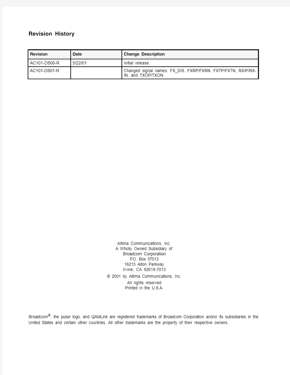
Revision History
Revision Date Change Description
AC101-DS00-R5/22/01Initial release.
AC101-DS01-R Changed signal names: FX_DIS, FXRP/FXRN, FXTP/FXTN, RXIP/RX-
IN, and TXOP/TXON.
Altima Communications, Inc.
A Wholly Owned Subsidiary of
Broadcom Corporation
P.O. Box 57013
16215 Alton Parkway
Irvine, CA 92619-7013
? 2001 by Altima Communications, Inc.
All rights reserved
Printed in the U.S.A.
Broadcom?, the pulse logo, and QAMLink are registered trademarks of Broadcom Corporation and/or its subsidiaries in the United States and certain other countries. All other trademarks are the property of their respective owners.
Preliminary Data Sheet I AC101 06/04/01
T ABLE OF C ONTENTS
Section 1: Functional Description (1)
Overview (1)
MAC Interface (1)
Media Independent Interface (MII) (1)
Serial Management Interface (SMI) (1)
Interrupts (2)
Carrier Sense/RX_DV (2)
7-Wire Serial Interface (2)
PCS Bypass (3)
100 Mbps PCS Bypass (3)
10 Mbps PCS Bypass (3)
Media Interface (3)
10BASE-T Interface (3)
Transmit Function (3)
Receive Function (3)
Link Monitor (3)
100BASE-TX Interface (3)
Transmit Function (4)
Parallel to Serial, NRZ to NRZI, and MLT3 Conversion (4)
Receive Function (4)
Baseline Wander Compensation (5)
Clock/Data Recovery (5)
Decoder/De-scrambler (5)
Link Monitor (5)
100BASE-FX Interface (6)
Transmit Function (6)
Receive Function (6)
Link Monitor (6)
Far-End-Fault-Insertion (FEFI) (6)
10BASE-T/100BASE-TX/FX Interface (6)
Multi-Mode Transmit Driver (6)
Adaptive Equalizer (7)
Broadcom
Document AC101-DS01-R¥¥¥¥¥Page iii
I AC101Preliminary Data Sheet
T ABLE OF C ONTENTS06/04/01 PLL Clock Synthesizer (7)
Jabber and SQE (Heartbeat) (7)
Reverse Polarity Detection and Correction (7)
Hardware Configuration (7)
Software Configuration (7)
LED Outputs (7)
Auto-Negotiation (8)
Parallel Detection (9)
Diagnostics (9)
Loopback Operation (9)
Cable Length Indicator (9)
Reset and Power (10)
Clock Input (10)
Section 2: Signal Definitions and Pin Assignments (11)
Pin Descriptions (11)
PHY Address Pins (11)
MDI (Media Dependent Interface) Pins (11)
MII (Media Independent Interface) 100 PCS Bypass Pins (12)
10 Mbps PCS Bypass Pins (13)
10 Mbps 7-Wire Interface Pins (13)
Special/Test Pins (14)
Control and Status Pins (14)
LED Indicators Pins (16)
Power and Ground Pins (17)
No Connect Pins (18)
Technology Selections (18)
Advanced LED Selections (19)
Section 3: Pinout Diagrams (21)
AC101QF Pinout Diagram (21)
AC101TF Pinout Diagram (22)
Section 4: Register Descriptions (23)
Register Summary (23)
MII-Specified Registers (24)
Broadcom
Page iv Document AC101-DS01-R¥¥¥¥¥
Preliminary Data Sheet I AC101 06/04/01T ABLE OF C ONTENTS
Register 0: Control Register (24)
Register 1: Status Register (25)
Register 2: PHY Identifier 1 Register (26)
Register 3: PHY Identifier 2 Register (26)
Register 4: Auto-Negotiation Advertisement Register (26)
Register 5: Auto-Negotiation Link Partner Ability Register (27)
Register 6: Auto-Negotiation Expansion Register (28)
Register 7: Auto-Negotiation Next Page Transmit Register (28)
Altima-Specified Registers (29)
Register 16: Polarity and Interrupt Level Register (29)
Register 17: Interrupt Control/Status Register (30)
Register 18: Diagnostic Register (30)
Register 19: Power/Loopback Register (31)
Register 20: Cable Measurement Register (31)
Register 21: Mode Control Register (32)
Register 24: Receive Error Counter Register (33)
4B/5B Code-Group Table (33)
SMI Read/Write Sequence (34)
Section 5: Electrical Characteristics (35)
Operating Range (35)
Total Power Consumption (35)
TTL I/O Characteristics (35)
REFCLK and XTAL Pin Characteristics (36)
I/O Characteristics – LED/CFG Pin Characteristics (36)
100BASE-TX Transceiver Characteristics (36)
10BASE-T Transceiver Characteristics (37)
100BASE-FX Transceiver Characteristics (37)
10BASE-T Link Integrity Timing Characteristics (38)
Section 6: Timing and AC Characteristics (39)
Digital Timing Characteristics (39)
Power on Reset Timing (39)
Management Data Interface Timing (39)
100BASE-TX/FX MII Transmit System Timing (40)
100BASE-TX/FX MII Receive System Timing (41)
Broadcom
Document AC101-DS01-R¥¥¥¥¥Page v
I AC101Preliminary Data Sheet
T ABLE OF C ONTENTS06/04/01 10BASE-T MII Transmit System Timing (42)
10BASE-T MII Receive System Timing (44)
10BASE-T 7-Wire Transmit System Timing (45)
10BASE-T 7-Wire Receive System Timing (46)
10BASE-T 7-Wire Collision Timing (46)
Recommended Board Circuitry (47)
TX Application Termination (47)
FX Application Termination (48)
Power and Ground Filtering for AC101QF (49)
Power and Ground Filtering for AC101TF (50)
Section 7: Mechanical Information (51)
Package Dimensions for AC101QF (100 pin PQFP) (51)
Package Dimensions for AC101TF (80 pin TQFP) (52)
Broadcom
Page vi Document AC101-DS01-R¥¥¥¥¥
Preliminary Data Sheet I AC101 06/04/01
L IST OF F IGURES
Figure 1:Functional Block Diagram (i)
Figure 2:Multifunction LED Pin Connection (19)
Figure 3:Dual-color LED Indicator for Link, Duplex, and Activity Status (20)
Figure 4:AC101QF Pinout Diagram (21)
Figure 5:AC101TF Pinout Diagram (22)
Figure 6:Power-on Reset Timing (39)
Figure 7:Management Data Interface Timing (40)
Figure 8:100BASE-TX/FX MII Transmit Timing (41)
Figure 9:100BASE-TX/FX MII Receive Timing (42)
Figure 10:10BASE-T MII Transmit Timing (43)
Figure 11:10BASE-T MII Receive Timing (44)
Figure 12:10BASE-T 7-WireTransmit Timing (45)
Figure 13:10BASE-T 7-Wire Receive Timing (46)
Figure 14:10BASE-T 7-Wire Collision Timing (47)
Figure 15:TX Application Termination Circuit (47)
Figure 16:FX Application Termination Circuit (48)
Figure 17:Power and Ground Filtering for the AC101QF (49)
Figure 18:Power and Ground Filtering for the AC101TF (50)
Figure 19:Package Dimensions for AC101QF (100 pin PQFP) (51)
Figure 20:Package Dimensions for AC101TF (80 pin TQFP) (52)
Broadcom
Document AC101-DS01-R¥¥¥¥¥Page vii
I AC101Preliminary Data Sheet
L IST OF F IGURES06/04/01
Broadcom
Page viii Document AC101-DS01-R¥¥¥¥¥
Preliminary Data Sheet I AC101 06/04/01
L IST OF T ABLES
Table 1:PHY Address Pins (11)
Table 2:MDI (Media Dependent) Pins (11)
Table 3:MII (Media Independent Interface) 100 PCS Bypass Pins (12)
Table 4:10 Mbps PCS Bypass Pins (13)
Table 5:10 Mbps 7-Wire Interface Pins (13)
Table 6:Special/Test Pins (14)
Table 7:Control and Status Pins (14)
Table 8:LED Indicator Pins (16)
Table 9:Power and Ground Pins (17)
Table 10:No Connect Pins (18)
Table 11:Technology Solutions (18)
Table 12:Advanced LED Selections (19)
Table 13:Register Summary (23)
Table 14:Register 0: Control Register (24)
Table 15:Register 1: Status Register (25)
Table 16:Register 2: PHY Identifier 1 Register (26)
Table 17:Register 3: PHY Identifier 2 Register (26)
Table 18:Register 4: Auto-Negotiation Advertisement Register (26)
Table 19:Register 5: Auto-Negotiation Link Partner Ability Register (27)
Table 20:Register 6: Auto-Negotiation Expansion Register (28)
Table 21:Register 7: Auto-Negotiation Next Page Transmit Register (28)
Table 22:Register 16: Polarity and Interrupt Level Register (29)
Table 23:Register 17: Interrupt Control/Status Register (30)
Table 24:Register 18: Diagnostic Register (30)
Table 25:Register 19: Power/Loopback Register (31)
Table 26:Register 20: Cable Measurement Register (31)
Table 27:Register 21: Mode Control Register (32)
Table 28:Register 24: Receive Error Counter Register (33)
Table 29:4B/5B Code-Group Table (33)
Table 30:SMI Read/Write Sequence (34)
Table 31:Total Power Consumption (35)
Table 32:TTL I/O Characteristics (35)
Broadcom
Document AC101-DS01-R¥¥¥¥¥Page ix
I AC101Preliminary Data Sheet
L IST OF T ABLES06/04/01 Table 33:REFCLK and XTAL Pin Characteristics (36)
Table 34:I/O Characteristics – LED/CFG Pin Characteristics (36)
Table 35:100BASE-TX Transceiver Characteristics (36)
Table 36:10BASE-T Transceiver Characteristics (37)
Table 37:100BASE-FX Transceiver Characteristics (37)
Table 39:Power On Reset Timing (39)
Table 40:Management Data Interface Timing (39)
Table 41:100BASE-TX/FX MII Transmit System Timing (40)
Table 42:100BASE-TX/FX MII Receive System Timing (41)
Table 43:10BASE-T MII Transmit System Timing (42)
Table 44:10BASE-T MII Receive System Timing (44)
Table 45:10BASE-T 7-Wire Transmit System Timing (45)
Table 46:10BASE-T 7-Wire Receive System Timing (46)
Table 47:10BASE-T 7-Wire Collision Timing (46)
Table 48:Quad Flat Pack Outline: 20 x 14 mm (51)
Table 49:Quad Flat Pack Outline: 12 x 12 mm (52)
Broadcom
Page x Document AC101-DS01-R¥¥¥¥¥
Preliminary Data Sheet I AC101 06/04/01
Section1:Functional Description
O VERVIEW
The AC101TF/QF PHYsical layer device (PHY) integrates the 100BASE-X and 10BASE-T functions in a single chip that is used in Fast Ethernet 10/100 Mbps applications. The 100BASE-X section consists of physical coding sublayer (PCS), phys-ical media attachment (PMA), and physical media dependent (PMD) functions and the 10BASE-T section consists of Manchester encoder/decoder (ENDEC) and transceiver functions. The device performs the following functions:
?4B/5B
?MLT3
?NRZI
?Manchester Encoding and Decoding
?Clock and Data Recovery
?Stream Cipher Scrambling/De-Scrambling
?Adaptive Equalization
?Line Transmission
?Carrier Sense
?Link Integrity Monitor
?Auto-Negotiation (ANeg)
?MII MAC connectivity
?MII Management Function
It also provides an IEEE802.3u compatible Media Independent Interface (MII) to communicate with an Ethernet Media Ac-cess Controller (MAC). Selection of 10 or 100 Mbps operation is based on the settings of internal Serial Management Inter-face registers or determined by the on-chip ANeg logic. The device can operate in 10 or 100 Mbps with full-duplex or half-duplex mode.
MAC I NTERFACE
M EDIA I NDEPENDENT I NTERFACE (MII)
The Media Independent Interface (MII) is an 18 wire MAC/PHY interface (see ”MII (Media Independent Interface) 100 PCS Bypass Pins” on page 12) described in 802.3u. The purpose of the interface is to allow MAC layer devices to attach to a variety of Physical Layer devices through a common interface. MII operates at either 100 Mbps or 10 Mbps, dependant on the speed of the Physical Layer. With clocks running at either 25 MHz or 2.5 MHz, 4 bit data is clocked between the MAC and PHY, synchronous with Enable and Error signals.
At the time of PLL lock on an incoming signal from the wire interface, the PHY will generate RX_CLK at either 2.5 MHz for 10 Mbps or 25 MHz for 100 Mpbs.
On receipt of valid data from the wire interface, RX_DV will go active signaling to the MAC that the valid data will be present-ed on the RXD[3:0] pins at the speed of the RX_CLK.
On transmission of data from the MAC, TX_EN is presented to the PHY indicating the presence of valid data on TXD[3:0]. TXD[3:0] are sampled by the PHY synchronous to TX_CLK during the time that TX_EN is valid.
Serial Management Interface (SMI)
The PHY’s internal registers are accessible only through the MII 2-wire Serial Management Interface (SMI. see ”MII (Media
Broadcom
Document AC101-DS01-R¥¥¥¥¥Overview Page 1
I AC101Preliminary Data Sheet
06/04/01
Independent Interface) 100 PCS Bypass Pins” on page 12). MDC is a clock input to the PHY which is used to latch in or out data and instructions for the PHY. The clock can run at any speed from DC to 25 MHz. MDIO is a bi-directional connection used to write instructions to, write data to, or read data from the PHY. Each data bit is latched either in or out on the rising edge of MDC. MDC is not required to maintain any speed or duty cycle, provided no half cycle is less than 20ns and that data is presented synchronous to MDC.
MDC/MDIO are a common signal pair to all PHYs on a design. Therefore, each PHY needs to have its own unique Physical Address. The Physical Address of the PHY is set using the pins defined as PHYAD[4:0] (see ”PHY Address Pins” on page 11). These input signals are strapped externally and sampled as reset is negated. At idle, the PHY is responsible to pull MDIO line to a high state. Therefore, a 1.5K Ohms resistor is required to connect MDIO line to Vcc. The PHYAD can be reprogrammed via software. A detailed definition of the Serial Management registers follows.
At the beginning of a read or write cycle, the MAC will send a continuous 32 bits of one at the MDC clock rate to indicate preamble. A zero and a one will follow to indicate start of frame. A read OP code is a one and a zero, while a write OP code is a zero and a one. These will be followed by 5 bits to indicate PHY address and 5 bits to indicate register address. Then 2 bits follow to allow for turn around time. For read operation, the first bit will be high impedance. Neither the PHY nor the station will assert this bit. During the second bit time, the PHY will assert this bit to a zero. For write operation, the station will drive a one for the first bit time, and a zero for the second bit time. The 16 bits data field is then presented. The first bit that is transmitted is bit 15 of the register content.
Interrupts
The INTR pin (see ”MII (Media Independent Interface) 100 PCS Bypass Pins” on page 12) on the PHY will be asserted when-ever one of 8 selectable interrupt events occur. Assertion state is programmable to either high or low through the INTR_LEVL register bit (see ”Register 16: Polarity and Interrupt Level Register” on page 29). Selection is made by setting the appropriate bit in the upper half of the Interrupt Control/Status register (see ”Register 17: Interrupt Control/Status Register” on page 30). When the INTR bit goes active, the MAC interface is required to read the Interrupt Control/Status register to determine which event caused the interrupt. The Status bits are read only and clear on read. When INTR is not asserted, the pin is held in a high impedance state.
Carrier Sense/RX_DV
Carrier sense is asserted asynchronously on the CRS pins as soon as activity is detected on the receive data stream. RX_DV is asserted as soon as a valid SSD (Start-of-Stream Delimiter) is detected. Carrier sense and RX_DV are de-assert-ed synchronously upon detection of a valid end of stream delimiter or two consecutive idle code groups in the receive data stream. However, if the carrier sense is asserted and a valid SSD is not detected immediately, RX_ER is asserted instead of RX_DV. See ”MII (Media Independent Interface) 100 PCS Bypass Pins” on page 12.)
In 10BASE-T mode, CRS is asserted asynchronously when the valid preamble and data activity is detected on the RXIP and RXIN pins.
In the half-duplex mode, the CRS is activated during the transmit and receiving of data. In the full-duplex mode, the CRS is activated during data reception only.
7-W IRE S ERIAL I NTERFACE
To allow the PHY to run in legacy 10 Mbps only designs, the 7-wire serial interface, referred to as General Purpose Serial Interface (GPSI, see ”10 Mbps 7-Wire Interface Pins” on page 13) has been included. GPSI is an industry standard interface which has been implemented in many micro-controllers and micro-processors, as well as the majority of the 10 Mpbs MACs.
The interface consists of 10 Mbps transmit and receive clocks, 10 Mbps serial transmit and receive data, transmit enable, receive enable and collision.
When running the GPSI mode, the PHY must be forced to 10 Mbps only mode through hardware configuration.
The 10BASE-T 7-wire interface is enabled when the GPIO[0] (see ”Control and Status Pins” on page 14) is pull low by 1 K?during reset.
Broadcom
Page 2MAC Interface Document AC101-DS01-R¥¥¥¥¥
Preliminary Data Sheet I AC101 06/04/01
PCS B YPASS
The AC101TF/QF is put into PCS bypass mode when the PCSBP pin is pull high (see ”Control and Status Pins” on page 14). 100 Mbps PCS Bypass
In MII designs, the encoding/decoding functions are performed in the PHY, thereby allowing 4-bit data exchange. Certain designs, however, require MAC/PHY data transfer to be in the form of 5-bit symbols. By selecting PCS Bypass mode of op-eration, the PHY will present data to, and accept data from the MAC layer as 5-bit symbols. In PCS Bypass mode the RX_ER and TX_ER pins are used as the RXD4 and TXD4 (see ”MII (Media Independent Interface) 100 PCS Bypass Pins” on page 12).
10 Mbps PCS Bypass
When using PCS Bypass at 10 Mbps, the standard MAC/PHY interface is no longer valid. Differential drivers and receivers carry data serially between the MAC and PHY (see ”10 Mbps PCS Bypass Pins” on page 13).
M EDIA I NTERFACE
The AC101TF/QF can be media-configured using any of the following three methods:
?Hardware configuration: see ”Control and Status Pins” on page 14.
?Software configuration: see ”Register 21: Mode Control Register” on page 32.
?Auto-Negotiation (ANeg): see ”Control and Status Pins” on page 14 and ”MII-Specified Registers” on page 24.
10BASE-T I NTERFACE
When configured to run in 10BASE-T mode, either through hardware configuration, software configuration, or ANeg, the PHY will support all the features and parameters of the industry standards.
Transmit Function
If the MII interface is used, Parallel to Serial logic is used to convert the 4-bit data into the serial stream. If the 7-Wire interface is used (see ”10 Mbps 7-Wire Interface Pins” on page 13), the serial data goes directly to the Manchester encoder where it is synthesized through the output waveshaping driver. The waveshaper reduces any EMI emission by filtering out the har-monics, therefore eliminating the need for an external filter.
Receive Function
The received signal passes through a low-pass filter, which filters out the noise from the cable, board, and transformer. This eliminates the need for a 10BASE-T external filter. A Manchester decoder converts the incoming serial stream. If the 7-wire 10BASE-T interface is enabled (see ”10 Mbps 7-Wire Interface Pins” on page 13), the decoded serial data is presented to the MAC. If the MII interface is used (see ”MII (Media Independent Interface) 100 PCS Bypass Pins” on page 12), Serial to Parallel logic is used to generate the 4-bit data.
Link Monitor
The 10-BASE-T link-pulse detection circuit will constantly monitor the RXIP/RXIN pins (see ”MDI (Media Dependent Inter-face) Pins” on page 11) for the presence of valid link pulses. In the absence of valid link pules, the Link Status bit will be cleared and the Link LED will de-assert.
100BASE-TX I NTERFACE
When configured to run in 100BASE-TX mode, either through hardware configuration, software configuration, or ANeg, the PHY will support all the features and parameters of the industry standards.
Broadcom
Document AC101-DS01-R¥¥¥¥¥Media Interface Page 3
I AC101Preliminary Data Sheet
06/04/01
Transmit Function
In 100BASE-TX mode, the PHY transmit function converts synchronous 4-bit data nibbles from the MII to a pair of 125 Mbps differential serial data streams. The serial data is transmitted over network twisted pair cables via an isolation transformer. Data conversion includes 4B/5B encoding, scrambling, parallel to serial, NRZ to NRZI, and MLT-3 encoding. The entire op-eration is synchronous to 25 MHz and 125 MHz clock. Both clocks are generated by an on-chip PLL clock synthesizer that is locked on to an external 25 MHz clock source.
The transmit data, in 4-bit nibbles at 25 MHz rate, is transmitted from the MAC to the PHY via the MII TXD[3:0] signals. The 4B/5B encoder replaces the first two nibbles of the preamble from the MAC frame with a /J/K/ code-group pair Start-of-Stream Delimiter (SSD), following the onset of TX_EN signal. The 4B/5B encoder appends a /T/R/ code-group pair End-of-Stream Delimiter (ESD) to the end of transmission in place of the first two IDLE code-groups that follow the negation of the TX_EN signal. The encapsulated data stream is converted from 4-bit nibbles to 5-bit code-groups. During the inter-packet gap, when there is no data present, a continuous stream of IDLE code-groups are transmitted. When TX_ER is asserted while TX_EN is active, the Transmit Error code-group /H/ is substituted for the translated 5B code word. The 4B/5B encoding is bypassed when Reg. 21.1 is set to “1”, or the PCSBP pin is strapped high. See ”MII (Media Independent Interface) 100 PCS Bypass Pins” on page 12.
In 100BASE-TX mode, the 5-bit transmit data stream is scrambled as defined by the TP-PMD Stream Cipher function in order to reduce radiated emissions on the twisted pair cable. The scrambler encodes a plain text NRZ bit stream using a key stream periodic sequence of 2047 bits generated by the recursive linear function:
X[n] = X[n-11] + X[n-9] (modulo 2)
The scrambler reduces peak emissions by randomly spreading the signal energy over the transmitted frequency range, thus eliminating peaks at any single frequency. For repeater applications, where all ports transmit the same data simultaneously, signal energy is spread further by using a non-repeating sequence for each PHY (i.e., the scrambled seed is unique for each different PHY based on the PHY address).
When Dis_Scrm (see ”Register 21: Mode Control Register” on page 32) is set to “0” the data scrambling function is disabled, the 5-bit data stream is clocked directly to the device’s PMA sublayer.
Parallel to Serial, NRZ to NRZI, and MLT3 Conversion
The 5-bit NRZ data is clocked into PHY’s shift register with a 25 MHz clock and clocked out with a 125 MHz clock to convert it into a serial bit stream. The serial data is converted from NRZ to NRZI format, which produces a transition on Logic 1 and no transition on Logic 0. To further reduce EMI emissions, the NRZI data is converted to an MLT-3 signal. The conversion offers a 3dB to 6dB reduction in EMI emissions. This allows system designers to meet the FCC Class B limit. Whenever there is a transition occurring in NRZI data, there is a corresponding transition occurring in the MLT-3 data. For NRZI data, it changes the count up/down direction after every single transition. For MLT-3 data, it changes the count up/down direction after every two transitions. The NRZI to MLT-3 data conversion is implemented without reference to the bit timing or clock information. The conversion requires detecting the transitions of the incoming NRZI data and setting the count up/down di-rection for the MLT-3 data. Asserting FX_SEL high will disable this encoding.
The slew rate of the transmitted MLT-3 signal can be controlled to reduce EMI emissions. The MLT-3 signal after the mag-netic has a typical rise/fall time of approximately 4 ns, which is within the target range specified in the ANSI TP- PMD stan-dard. This is guaranteed with either 1:1 or 1.25:1 transformer.
Receive Function
The 100BASE-TX receive path functions as the inverse of the transmit path. The receive path includes a receiver with adap-tive equalization and DC restoration in the front end. It also includes a MLT-3 to NRZI converter, 125 MHz data and clock recovery, NRZI/NRZ conversion, Serial-to-Parallel conversion, de-scrambler, and 5B/4B decoder. The receiver circuit starts with a DC bias for the differential RX+/- inputs, followed with a low-pass filter to filter out high frequency noise from the trans-mission channel media. An energy detect circuit is also added to determine whether there is any signal energy on the media. This is useful in the power-saving mode. The amplification ratio and slicer’s threshold is set by the on-chip bandgap refer-ence.
Broadcom
Page 4Media Interface Document AC101-DS01-R¥¥¥¥¥
Preliminary Data Sheet I AC101 06/04/01
Baseline Wander Compensation
The 100BASE-TX data stream is not always DC balanced. The transformer blocks the DC components of the incoming sig-nal, thus the DC offset of the differential receive inputs can drift. The shifting of the signal level, coupled with non-zero rise and fall times of the serial stream can cause pulse-width distortion. This creates jitter and possible increase in the bit error rates. Therefore, a DC restoration circuit is needed to compensate for the attenuation of the DC component. This PHY im-plements a patent-pending DC restoration circuit. Unlike the traditional implementation, the circuit does not need the feed-back information from the slicer or the clock recovery circuit. This design simplifies the circuit design and eliminates any random/systematic offset on the receive path. In the 10BaseT and the 100BASE-FX modes, the baseline wander correction circuit is not required, and therefore is disabled.
Clock/Data Recovery
The equalized MLT-3 signal passes through the slicer circuit, and gets converted to NRZI format. The PHY uses a propri-etary mixed-signal phase locked loop (PLL) to extract clock information from the incoming NRZI data. The extracted clock is used to re-time the data stream and set the data boundaries. The transmit clock is locked to the 25 MHz clock input while the receive clock is locked to the incoming data streams. When initial lock is achieved, the PLL switches to the data stream, extracts the 125 MHz clock, and uses it for the bit framing for the recovered data. The recovered 125 MHz clock is also used to generate the 25 MHz RX_CLK signal. The PLL requires no external components for its operation and has high noise im-munity and low jitter. It provides fast phase alignment and locks to data in one transition. Its data/clock acquisition time after power-on is less than 60 transitions. The PLL can maintain lock on run-lengths of up to 60 data bits in the absence of signal transitions. When no valid data is present, i.e. when the SD is de-asserted, the PLL will switch and lock on to TX_CLK. This provides a continuously running RX_CLK. At the PCS interface, the 5 bit data RXD[4:0] is synchronized to the 25 MHz RX_CLK. See ”MII (Media Independent Interface) 100 PCS Bypass Pins” on page 12.
Decoder/De-scrambler
The de-scrambler detects the state of the transmit Linear Feedback Shift Register (LFSR) by looking for a sequence repre-senting consecutive idle codes. The de-scrambler acquires lock on the data stream by recognizing IDLE bursts of 30 or more bits and locks its frequency to its de-ciphering LFSR.
Once lock is acquired, the device can operate with an inter-packet-gap (IPG) as low as 40 nS. However, before lock is ac-quired, the de-scrambler needs a minimum of 270 nS of consecutive idles in between packets in order to acquire lock.
The de-ciphering logic also tracks the number of consecutive errors received while the RX_DV (see ”MII (Media Independent Interface) 100 PCS Bypass Pins” on page 12) is asserted. Once the error counter exceeds its limit currently set to 64 con-secutive errors, the logic assumes that the lock has been lost, and the de-cipher circuit resets itself. The process of regaining lock will start again.
Stream cipher de-scrambler is not used in the 100BASE-FX and the 10BASE-T modes.
Link Monitor
Signal level is detected through a squelch detection circuitry. A signal detect (SD) circuit allows the equalizer to assert high whenever the peak detector detects a post-equalized signal with peak to ground voltage greater than 400 mV. This is ap-proximately 40% of a normal signal voltage level. In addition, the energy level must be sustained for longer than 2~3 μS in order for the signal detect signal to stay on. The SD gets de-asserted approximately 1~2 μs after the energy level drops consistently below 300 mV from peak to ground.
The link signal is forced low during a local loopback operation (Loopback register bit is set) and forced to high when a remote loopback is taking place (EN_RPBK is set, see ”Register 21: Mode Control Register” on page 32).
In forced 100BASE-TX mode, when a cable is unplugged or no valid signal is detected on the receive pair, the link monitor enters in the “link fail” state and NLP's are transmitted. When a valid signal is detected for a minimum period of time, the link monitor enters Link Pass State and transmits MLT-3 signal.
Broadcom
Document AC101-DS01-R¥¥¥¥¥Media Interface Page 5
I AC101Preliminary Data Sheet
06/04/01
100BASE-FX I NTERFACE
When configured to run in 100BASE-FX mode, either through hardware configuration or software configuration (100BASE-FX does not support ANeg) the PHY will support all the features and parameters of the industry standards.
Transmit Function
The serialized data bypasses the scrambler and 4B/5B encoder in FX mode. The output data is NRZI PECL signals. The PECL level signals are used to drive the Fiber-transmitter.
Receive Function
In 100BASE-FX mode, signal is received through the PECL receiver inputs, and directly passed to the clock recovery circuit for data/clock extraction. In FX mode, the scrambler/de-scrambler cipher function is bypassed.
Link Monitor
In 100BASE-FX mode, the external fiber-optic receiver performs the signal energy detection function and communicates this information directly to the PHY’s SDP pin (see ”MDI (Media Dependent Interface) Pins” on page 11).
Far-End-Fault-Insertion (FEFI)
ANeg provides the mechanism to inform the link partner that a remote fault has occurred. However, ANeg is disabled in the 100BASE-FX applications. An alternative in-band signaling function (FEFI) is used to signal a remote fault condition. FEFI is a stream of 84 consecutive ones followed by one logic zero. This pattern is repeated 3 times. A FEFI will signal under 3 conditions:
1When no activity is received from the link partner.
2When the clock recovery circuit detects a signal error or PLL lock error.
3When management entity sets the transmit Far-End-Fault bit.
The FEFI mechanism is enabled by default in the 100BASE-FX mode, and is disabled in 100BASE-TX or 10BASE-T modes. The register setting can be changed by software after reset.
10BASE-T/100BASE-TX/FX I NTERFACE
Multi-Mode Transmit Driver
The multi-mode driver transmits the MLT-3 coded signal in 100BASE-TX mode, NRZI coded signal in 100BASE-FX mode, and Manchester coded signal in 10BASE-T mode.
In 100BASE-FX mode, no filtering is performed. The transmit driver utilizes a current drive output which is well balanced and produces a low noise PECL signal. PECL voltage levels are produced with resistive terminations. (See section 16.)
In 10BaseT mode, high frequency pre-emphasis is performed to extend the cable-driving distance without the external filter. The FLP and NLP pulses are also drive out through the 10BaseT driver.
The 10BaseT and 100BaseTX transmit signals are multiplexed to the transmit output driver. This arrangement results in us-ing the same external transformer for both the 10BaseT and the 100BaseTX. The driver output level is set by a built-in band-gap reference and an external resistor connected to the RIBB pin (see ”Special/Test Pins” on page 14). The resistor sets the output current for all modes of operation. The TXOP/N outputs (see ”MDI (Media Dependent Interface) Pins” on page 11) are open drain devices with serial source to I/O pad resistance of 10 ? maximum. When the 1:1 transformer is used, the current rating is 40 mA for the 2V p-p MLT-3 signal, and 100 mA for the 5V p-p Manchester signal. One can use a 1.25:1 trans-mit transformer for a 20% output driver power reduction. This will decrease the drive current to 32 mA for 100BASE-TX op-eration, and 80 mA for 10BASE-T operation.
Broadcom
Page 6Media Interface Document AC101-DS01-R¥¥¥¥¥
Preliminary Data Sheet I AC101 06/04/01
Adaptive Equalizer
The PHY is designed to accommodate a maximum of 150 meters UTP CAT-5 cable. An AT&T 1061 CAT-5 cable of this length typically has an attenuation of 31 dB at 100 MHz. A typical attenuation of 100-meter cable is 21 dB. The worst case cable attenuation is around 24-26 dB as defined by TP-PMD specification.
The amplitude and phase distortion from the cable cause inter-symbol interference (ISI) which makes clock and data recov-ery difficult. The adaptive equalizer is designed to closely match the inverse transfer function of the twisted-pair cable. The equalizer has the ability to changes its equalizer frequency response according to the cable length. The equalizer will tune itself automatically for any cable, compensating for the amplitude and phase distortion introduced by the cable.
PLL Clock Synthesizer
The PHY includes an on-chip PLL clock synthesizer that generate 25 MHz and 125 MHz clocks for the 100BASE-TX circuit-ry. It also generates 20 MHz and 100 MHz clocks for the 10BaseT and ANeg circuitry. The PLL clock generator uses a fully differential VCO cell that introduces very low jitter. The Zero Dead Zone Phase Detection method implemented in the PHY design provides excellent phase tracking. A charge pump with charge sharing compensation is also included to further re-duce jitter at different loop filter voltages. The on-chip loop filter eliminates the need for external components and minimizes the external noise sensitivity. Only one external 25 MHz crystal or clock source is required as a reference clock.
After power-on or reset, the PLL clock synthesizer generates the 20 MHz clock output until the 100BASE-X operation mode is selected.
Jabber and SQE (Heartbeat)
After the MAC transmitter exceeds the jabber timer (46mS), the transmit and loopback functions will be disabled and COL signal get asserted. After TX_EN goes low for more than 500 ms, the TP transmitter will reactivate and COL gets de-assert-ed. Setting Jabber Disable will disable the jabber function.
When the SQE test is enabled, a COL pulse with 5-15BT is asserted after each transmitted packet. SQE is enabled in 10BASE-T by default, and can be disabled via SQE Test Inhibit.
Reverse Polarity Detection and Correction
Certain cable plants have crossed wiring on the twisted pairs; the reversal of TXIN and TXIP. Under normal circumstances this would cause the receive circuitry to reject all data. When the Auto Polarity Disable bit (see ”Register 16: Polarity and Interrupt Level Register” on page 29) is cleared, the PHY has the ability to detect the fact that either 8 NLPs or a burst of FLPs are inverted and automatically reverse the receiver’s polarity. The polarity state is stored in the Reverse Polarity bit.
If the Auto Polarity Disable bit is set, then the Reverse Polarity bit (see ”Register 16: Polarity and Interrupt Level Register”on page 29) can be written to force the polarity reversal of the receiver.Initialization and Setup
H ARDWARE C ONFIGURATION
Several different states of operation can be chosen through hardware configuration. External pins may be pulled either high or low at reset time (see ”Control and Status Pins” on page 14). The combination of high and low values determines the power on state of the device.
Many of these pins are multi-function pins which change their meaning when reset ends.
S OFTWARE C ONFIGURATION
Several different states of operation can be chosen through software configuration. Please refer to ”Serial Management In-terface (SMI)” on page 1 and Section 4 ”Register Descriptions” on page 23.
LED Outputs
Individual LED outputs are available to indicate Speed, Duplex, Collision, Receive, Transmit, and Link. These multi-function pins are inputs during reset and LED output pins thereafter. The level of these pins during reset determines their active out-
Broadcom
Document AC101-DS01-R¥¥¥¥¥Media Interface Page 7
I AC101Preliminary Data Sheet
06/04/01
put states. If a multi-function pin is pulled up during reset to select a particular function, then that LED output would become active low, and the LED circuit must be designed accordingly, and vice versa.
In addition to the individual LED configurations, an advanced LED circuit has been implemented, as illustrated in ”Advanced LED Selections” on page 19.
A UTO-N EGOTIATION
By definition the 10/100 Transceiver is able to run at either 10 Mbps over Twisted Pair Copper (10BASE-T), 100 Mpbs over Twisted Pair Copper (100BASE-TX) or 100 Mpbs over Fiber Optics (100BASE-FX). In addition the PHY is able to run in either half-duplex (repeater mode) or full-duplex. To determine the operational state, the PHY has hardware selects and soft-ware selects while also supporting Auto- Negotiation and Parallel Detection. To run in 100BASE-FX mode, the selection must be done through hardware configuration. There is no support for Auto-Negotiation of the FX interface.
Not all of the above combinations are possible due to limitations of the environment and the 802.3 standards. Legitimate operating states are:
?10BASE-T Half-duplex
?10BASE-T Full-duplex
?100BASE-TX Half-duplex
?100BASE-TX Full-duplex
?100BASE-FX Half-duplex
?100BASE-FX Full-duplex
The PHY can be hardware configured to force any one of the above mentioned modes (see ”Control and Status Pins” on page 14). By forcing the mode, the PHY will only run in that mode, hence limiting the locations where the product will operate.
The PHY is able to negotiate its mode of operation in the twisted pair environment using the Auto-Negotiation mechanism defined in the clause 28 of IEEE 802.3u specification. ANeg can be enabled or disabled by hardware (ANEGA pin) or soft-ware (Reg. 0.12) control. When the ANeg is enabled,the PHY chooses its mode of operation by advertising its abilities and comparing them with the ability received from its link partner. It can be configured to advertise 100BASE-TX or 10BASE-T operating in either full or half-duplex.
Register 4 (see ”Register 4: Auto-Negotiation Advertisement Register” on page 26) contains the current capabilities, speed and duplex, of the PHY, determined through hardware selects (TECH[2:0], see ”Control and Status Pins” on page 14) or chip defaults. The contents of Reg. 4 is sent to its link partner during the ANeg process using Fast Link Pulses (FLPs). An FLP is a string of 1s and 0s, each of which has a particular meaning, the total of which is called a Link Code Word. After reset, software can change any of these bits from 1 to 0 and back to 1, but not from 0 to 1. Therefore, the hardware has priority over software.
When ANeg is enabled, the PHY sends out FLPs during the following conditions:
?Power on
?Link loss
?Restart command
During this period, the PHY continually sends out FLPs while monitoring the incoming FLPs from the link partner to deter-mine their optimal mode of operation. If FLPs are not detected during this phase of operation, Parallel Detection mode is entered (see ”Parallel Detection” on page 9).
When the PHY receives 3 identical link code words (ignoring acknowledge bit) from its link partner, it stores these code words in Reg. 5 (see ”Register 5: Auto-Negotiation Link Partner Ability Register” on page 27), sets the acknowledge bit it the gen-erated FLPs, and waits to receive 3 identical code word with the acknowledge bit set from the link partner. Once this occurs the PHY configures itself to the highest technology that is common to both ends.
Broadcom
Page 8Media Interface Document AC101-DS01-R¥¥¥¥¥
Preliminary Data Sheet I AC101 06/04/01
The technology priorities are:
1100BASE-TX, full-duplex
2100BASE-TX, half-duplex
310BASE-T, full-duplex
410BASE-T half-duplex
Once the ANeg is complete, Reg. 1.5 is set, Reg. 1.[14:11] reflects negotiated speed and duplex mode, and the PHY enters the negotiated transmission and reception state. This state will not change until link is lost or the PHY is reset through either hardware or software, or the restart negotiation bit (Reg. 0.9) is set. See ”Register 0: Control Register” on page 24 and ”Reg-ister 1: Status Register” on page 25.
P ARALLEL D ETECTION
Because there are many devices in the field that do not support the ANeg process, but must still be communicated with, it is necessary to detect and link through the Parallel Detection process.
The parallel detection circuit is enabled in the absence of FLPs. The circuit is able to detect:
?Normal Link Pulse (NLP)
?10BASE-T receive data
?100BASE-TX idle
The mode of operation gets configured based on the technology of the incoming signal. If any of the above is detected, the device automatically configures to match the detected operating speed in the half-duplex mode. This ability allows the device to communicate with the legacy 10BASE-T and 100BASE-TX systems, while maintaining the flexibility of Auto-Negotiation.
D IAGNOSTICS
Loopback Operation
Local Loopback and Remote Loopback are provided for testing purpose. They can be enabled by write to either Reg. 0.14 (LPBK) or Reg. 21.3 (EN_RPBK). See ”Register 0: Control Register” on page 24 and ”Register 21: Mode Control Register”on page 32.
The Local Loopback routes transmitted data through the transmit path back to the receiving path’s clock and data recovery module. The loopback data are presented to the PCS in 5 bits symbol format. This loopback is used to check the operation of the 5-bit symbol decoder and the phase locked loop circuitry. In Local Loopback, the SD output is forced to logic one and TXOP/N outputs are tri-stated.
In Remote Loopback, incoming data is passed through the equalizer and clock recovery, then looped back to the NRZI/MLT3 converter and then to the transmit driver. This loopback is used to ensure the device’s connection on the media side. It also checks the operation of the device's internal adaptive equalizer, phase locked loop circuit, and wave-shaper synthesizer. During Remote Loopback, signal detect (SD) output is forced to logic zero.
Cable Length Indicator
The PHY can detect the length of the cable it’s attached and display the result in Reg. 20.[7:4] (see ”Register 20: Cable Mea-surement Register” on page 31). A reading of [0000] translates to < 10m cable used, [0001] translates to ~ 10 meter of cable, and [1111] translates to 150 meter cable. The cable length value can be used by the network manage to determine the prop-er connectivity of the cable and to manage the cable plant distribution
Broadcom
Document AC101-DS01-R¥¥¥¥¥Media Interface Page 9
I AC101Preliminary Data Sheet
06/04/01
R ESET AND P OWER
The PHY can be reset in three ways:
1During initial power on.
2Hardware Reset: (See pin descriptions).
3Software Reset: (See register descriptions).
The power consumption of the device is significantly reduced due to its built-in power management features. Separate power supply lines are used to power the 10BaseT circuitry and the 100BaseTX circuitry. Therefore, the two circuits can be turned-on and turned-off independently. When the PHY is set to operate in 100BASE-TX mode, the 10BASE-T circuitry is powered down, and vice versa.
The following power management features are supported:
1Power down mode: (See Section 2 ”Signal Definitions and Pin Assignments” on page 11 and Section 4 ”Register De-scriptions” on page 23). During power down mode, the device is still be able to interface through the management inter-face.
2Energy detect/power saving mode: Energy detect mode turns off the power to select internal circuitry when there is no live network connected. Energy Detect (ED) circuit is always turned on to monitor if there is a signal energy present on the media. The management circuitry is also powered on and ready to respond to any management transaction. The transmit circuit still send out link pulses with minimum power consumption. If a valid signal is received from the media, the device will power up and resume normal transmit/receive operation.
3Valid data detection mode: This can be achieved by writing to the Receive Clock Register Control Bit. During this mode, if there is no data other than idles coming in, the receive clock (RX_CLK, see ”MII (Media Independent Interface) 100 PCS Bypass Pins” on page 12) will turn off. This could save the power of the attached media access controller. RX_CLK will resume operation one clock period prior to the assertion of RX_DV. The receive clock will again shut off 64 clock cycles after RX_DV gets de-asserted.
4Reduced Transmit Drive Strength mode: Additional power saving can be gained at the PHY level by designing with
1.25:1 turns ration magnetic (see pin and register descriptions).
C LOCK I NPUT
The clock input (see ”Special/Test Pins” on page 14) can be either a TTL clock oscillator or a crystal measured at 25 MHz-100PPM.
Broadcom
Page 10Reset and Power Document AC101-DS01-R¥¥¥¥¥
以太网标准和物理层及数据链路层专题
资料编码产品名称 使用对象产品版本 编写部门资料版本 以太网标准和物理层、数据链路层专题 拟制:日期: 审核:日期: 审核:日期: 批准:日期: 华为技术有限公司 版权所有侵权必究 修订记录 日期修订版本作者描述
目录 1 以太网标准 5 1.1 以太网标准 5 1.2 IEEE标准 5 1.3 物理层 8 1.3.1 以太网接口类型 8 1.3.2 电口 8 1.3.3 光口 11 1.4 FE自协商 12 1.4.1 自协商技术的功能规范 13 1.4.2 自协商技术中的信息编码 14 1.4.3 自协商功能的寄存器控制 16 1.4.4 GE自协商 18 1.5 物理层芯片和MAC层芯片接口简介 19 1.5.1 MII 19 1.5.2 MDIO管理寄存器 20 1.5.3 RMII 20
1.5.4 SMII 21 1.5.5 SS-SMII 21 1.5.6 GMII 22 1.5.7 TBI 22 2 以太网数据链路层 23 2.1 以太网的帧格式 23 2.2 以太网的MAC地址 25 2.3 CSMA/CD算法 26 2.3.1 CSMA/CD发送过程 27 2.3.2 CSMA/CD如何接收 28 2.4 半双工以太网的限制 31 2.5 以太网流量控制 34 2.5.1 反压(Backpressure) 34 2.5.2 PAUSE 流控 34 关键词: 以太网物理层数据链路局域网城域网协议标准祯结构
摘要: 本文详细地阐述了以太网的标准,以太网在各个传输层面的具体结构和工作方式以及控制方式。 缩略语清单: 无。 参考资料清单 无。 以太网标准和物理层、数据链路层专题 1 以太网标准 1.1 以太网标准 局域网(LAN)技术用于连接距离较近的计算机,如在单个建筑或类似校园的集中建筑中。城市区域网(MAN)是基于10-100Km的大范围距离设计的,因此需要增强其可靠性。但随着通信的发展,从技术上看,局域网和城域网有融合贯通的趋势。 1.2 IEEE标准 IEEE是电气和电子工程师协会(Institute of Electrical and Electronics Engineers)的简称,IEEE组织主要负责有关电子和电气产品的各种标准的制定。IEEE于1980年2月成立了IEEE 802委员会,专门研究和指定有关局域网的各种标准。IEEE 802委员会由6个分委员会组成,其编号分别为802.1
第二、三章 以太网标准和物理层
修订记录 第二章以太网标准 目标: 了解以太网标准结构。 熟悉各以太网标准定义的内容 一、以太网标准 局域网(LAN)技术用于连接距离较近的计算机,如在单个建筑或类似校园的集中建筑中。城市区域网(MAN)是基于10-100Km的大范围距离设计的,因此需要增强其可靠性。但随着通信的发展,从技术上看,局域网和城域网有融合贯通的趋势。 IEEE是电气和电子工程师协会(Institute of Electrical and Electronics Engineers)的简称,IEEE组织主要负责有关电子和电气产品的各种标准的制定。 IEEE于1980年2月成立了IEEE 802委员会,专门研究和指定有关局域网的各种标准。IEEE 802委员会由6个分委员会组成,其编号分别为802.1至802.6,其标准分别称为标准802.1至标准802.6,目前它已增加到12个委员会,这些分委员会的职能如下: ·802.1--高层及其交互工作。提供高层标准的框架,包括端到端协议、网络互 连、网络管理、路由选择、桥接和性能测量。 ·802.2--连接链路控制LLC,提供OSI数据链路层的高子层功能,提供LAN 、 MAC子层与高层协议间的一致接口。 ·802.3--以太网规范,定义CSMA/CD标准的媒体访问控制(MAC)子层和物理 层规范。 ·802.4--令牌总线网。定义令牌传递总线的媒体访问控制(MAC)子层和物理 层规范。 ·802.5--令牌环线网,定义令牌传递环的媒体访问控制(MAC)子层和物理层 规范。 ·802.6--城域网MAN,定义城域网(MAN)的媒体访问控制(MAC)子层和物理
RMII模式以太网PHY芯片DP83848C的应用
引言 DP83848C是美国国家半导体公司生产的一款鲁棒性好、功能全、功耗低的10/100 Mbps单路物理层(PHY)器件。它支持MII(介质无关接口)和RMII(精简的介质无关接口),使设计更简单灵活;同时,支持10BASE~T和100BASE-TX以太网外设,对其他标准以太网解决方案有良好的兼容性和通用性。 MII(Medium Independent Interface)是IEEE802.3u规定的一种介质无关接口,主要作用是连接介质访问控制层(MAC)子层与物理层(PH-Y)之间的标准以太网接口,负责MAC 和PHY之间的通信。由于MII需要多达16根信号线,由此产生的I/O口需求及功耗较大,有必要对MII引脚数进行简化,因此提出了RMII(Reduced Medium Independent Interface,精简的介质无关接口),即简化了的MII。 1 硬件设计 1.1 电路设计 DP83848C的收发线路各是一对差分线,经过变比为1:1的以太网变压器后与网线相连。以太网变压器的主要作用是阻抗匹配、信号整形、网络隔离,以及滤除网络和设备双方面的噪音。典型应用如图1所示。 图2是DP83848C与MAC的连接电路。其中,Xl为50 MHz的有源振荡器。
1.2 PCB布局布线 布局方面,精度为1%的49.9 Ω电阻和100 nF的去耦电容应靠近PHY器件放置,并通过最短的路径到电源。如图3所示,两对差分信号(TD和RD)应平行走线,避免短截,且尽量保证长度匹配,这样可以避免共模噪声和EMI辐射。理想情况下,信号线上不应有交叉或者通孔,通孔会造成阻抗的非连续性,所以应将其数目降到最低;同时,差分线应尽可能走在一面,且不应将信号线跨越分割的平面,如图4所示。信号跨越一个分割的平面会造成无法预测的回路电流,极可能导致信号质量恶化并产生EMI问题。注意,图3和图4中,阴影部分为错误方法。 2 RMll模式描述 RMII模式在保持物理层器件现有特性的前提下减少了PHY的连接引脚。
以太网信号质量问题之收发器驱动偏置电阻的处理
以太网信号质量问题之收发器驱动偏置电阻的处理 一前言 对于系统设计人员来说,模数混合电路中最困难的地方在于模拟部分的设计,其中最具代表性的就是我们经常要面对的物理层收发器(PHY)及其收发回路和匹配网络的设计。即使对于应用比较成熟的以太网物理层设计而言,DA C驱动电流的基准偏置,差分信号线对的走线,乃至于匹配电阻的位置,都有可能影响到其物理层的信号质量并通过接口技术指标测试暴露出来。 二以太网口信号质量测试分析 1 100Base-TX接口测试环境及其设置 100Base-TX接口测试原理 100Base-TX接口的测试采用业内比较通用的诱导发包的
方法来引导DUT发出扰码后的IDLE进行测试,更多细节请参考美国力科公司《Ethernet solution-QualiPHY》专项技术文档, 测试设备: 测试拓扑如图1:
图1 Ethernet接口指标测 试连接框图 2 测试中出现的问题 本次测试将主要验证产品上4个以太网100Base-TX接口的技术指标。对于其中比较直观的100Base-TX物理层的眼图模板,《ANSI+X3_263-1995》标准中有着明确的眼图模板定义见图2。 图2 100Base-TX 眼图模板 关于100Base-TX接口技术指标的测试方法,《IEEE Std 802.3-2000》标准中也有详细的说明,工程师按照诱导发包的测试方法进行了网口眼图的测试,测试过程中
发现测试网口出现了信号波形碰触模板的问题,波形见图3: 图3 以太网口测试眼图_FAIL 3 问题分析解决 从眼图初步分析来看,发送信号的幅度应该是满足要求的。但是可以明显的发现信号边沿还是比较缓,而且从单个波形来看边沿有不单调的问题。方案的原厂是一家通讯业内专注于IP宽带解决方案的国际型大公司,其以太网模块部分应该经过详细验证过。最大的可能是二次开发过程中板级系统设计时的一些关键技术参数的配合问题。工程师在进行了信号幅度以及上升下降时间等细节指标的
工业以太网通信协议研究及应用
工业以太网通信协议研究及应用 发表时间:2018-04-24T14:54:01.377Z 来源:《防护工程》2017年第36期作者:林立胜 [导读] Modbus/TCP是用于控制和管理自动化设备的Modbus系列通讯协议的派生产品。 南京富岛软件公司 210032 摘要:在绝大多数工业控制通信方面都是采用现场总线技术方式来实现的。但长期以来现场总线种类繁多、同时又没有统一标准而导致互不兼容,使得系统集成和信息集成面临着巨大挑战,所以引入了应用广泛、高速率、低成本的以太网技术。但以太网的可靠性和实时性比较差,难以适应工业控制的要求,故相关组织对以太网进行了一些扩展,称为工业以太网。随着工业4.0的发展,相信工业以太网技术将越来越重要。本文就常见工业以太网通信协议简介及应用作出阐述。 关键词:现场总线技术、工业以太网、EtherCat、Ethernet/IP、ProfiNet、Modbus/TCP、Ethernet/PowerLink、MechatroLink 1常见工业以太网通信协议 1.1、Modbus/TCP Modbus/TCP是用于控制和管理自动化设备的Modbus系列通讯协议的派生产品。 由此可见,它覆盖了使用TCP/IP协议的Intranet企业内部网和Internet互联网环境中Modbus报文的用途。 该协议的最常见用途是为例如I/O、PLC模块以及连接其它简单域总线或I/O模块的网关服务的。 Modbus/TCP协议是作为一种实际的自动化标准发行的。既然Modbus已经广为人知,该规范只将别处没有收录的少量信息列入其中。 然而该规范力图阐明Modbus中哪种功能对于普通自动化设备的互用性有价值,哪些部分是Modbus作为可编程的协议交替用于PLC的多余部分。 Modbus/TCP 在美国比较流行,它由两部分组成,即IDA分散式控制系统的结构与Modbus/TCP 的信息结构的结合。Modbus/TCP定义了一个简单的开放式又广泛应用的传输协议网络用于主从通讯方式。 1.2.、Ethernet/IP Ethernet/IP是一个面向工业自动化应用的工业应用层协议,这里的IP表示Industrial-Protocal。 它建立在标准UDP/IP与TCP/IP协议之上,利用固定的以太网硬件和软件,为配置、访问和控制工业自动化设备定义了一个应用层协议。Ethernet/IP是在应用层提高了以太网的实时性。 1.3、EnterCat EtherCat以太网控制自动化技术是一个以Ethernet以太网为基础的开放架构的现场总线系统。 EtherCat名称中的Cat为Control Automation Technology控制自动化技术首字母的缩写,最初由德国倍福自动化有限公司BeckhoffAutomationGmbH研发。 EtherCat为拓扑的灵活性和系统的实时性能树立了新的标准,同时它还符合甚至降低了现场总线的使用成本。EtherCAT的特点还包括可选线缆冗余、功能性安全协议(SIL3)和高精度设备同步。 EtherCat通过协议内部的优先权机制可区别传输数据的优先权(Process Data),组态数据或参数的传输是在一个确定的时间段中通过一个专用的服务通道进行(Acyclic Data),EtherCat操作系统的以太网功能与传输的IP协议兼容。 EtherCat设备分从站和主站,从站一般是伺服驱动器、IO模块、板卡、网关等等,主站通常是运动控制器等。 1.4、Ethernet/PowerLink 鉴于以太网的蓬勃发展和CanOpen在自动化领域的广阔应用基础,Ethernet/PowerLink融合了这两项技术的优缺点,既拥有Ethernet 的开放性、高速接口,又参考了CanOpen在工业领域良好的PDO和SDO数据定义; 在某种意义上说Ethernet/PowerLink就是Ethernet上的CanOpen,在物理层、数据链路层使用了Ethernet介质,而应用层则保留了原有的PDO和SDO对象字典的结构。 Ethernet/PowerLink主攻方面是同步驱动和特殊设备的驱动要求。 1.5、MechatroLink MechatroLink是一个用在工业自动化的开放式通讯协定,最早由安川电机开发,现在则由MechatroLink协会Mechatrolink Members Association维护。 MechatroLink协议分为两种: MechatroLink-III,定义传送接口为以太网的通讯协定架构,速度最快为100Mbit/s,允许最多62个从站。 MechatroLink-II,定义传送接口为RS-485的通讯协定架构,速度最快为10Mbit/s,允许最多30个从站; MechatroLink的目标领域主要是以运动控制为中心的现场网络,可连接的设备包括CNC、PLC、PC卡、运动控制器、变频器、外围图像处理设备、伺服驱动器、外围IO设备等。 MechatroLink协会的主要成员基本上都是日本的自动控制厂商,包括欧姆龙、横河电机、安川电机等。 1.6、ProfiNet ProfiNet由西门子主导的Profibus国际组织ProfiBus International-PI推出,是基于工业以太网技术的自动化总线标准。 作为一项战略性的技术创新,ProfiNet为自动化通信领域提供了一个完整的网络解决方案,涵括了例如运动控制、实时以太网、网络安全、分布式自动化以及故障安全等当前自动化领域的热点话题; 作为跨供应商的技术,ProfiNet可以完全兼容工业以太网和现有的现场总线如ProfiBus技术,保护现有投资。 ProfiNet是适用于不同需求的完整解决方案,其功能包括8个主要的模块,依次为运动控制、分布式自动化、网络安装、实时通信、IT 标准和信息安全、故障安全、过程自动化和分布式现场设备。
以太网物理层信号测试与分析报告
以太网物理层信号测试与分析 1 物理层信号特点 以太网对应OSI七层模型的数据链路层和物理层,对应数据链路层的部分又分为逻辑链路控制子层(LLC)和介质访问控制子层(MAC)。MAC与物理层连接的接口称作介质无关接口(MII)。物理层与实际物理介质之间的接口称作介质相关接口(MDI)。在物理层中,又可以分为物理编码子层(PCS)、物理介质连接子层(PMA)、物理介质相关子层(PMD)。根据介质传输数据率的不同,以太网电接口可分为10Base-T,100Base-Tx和1000Base-T三种,分别对应10Mbps,100Mbps和1000Mbps三种速率级别。不仅是速率的差异,同时由于采用了不同的物理层编码规则而导致对应的测试和分析方案也全然不同,各有各的章法。下面先就这三种类型以太网的物理层编码规则做一分析。 1、1 10Base-T 编码方法 10M以太网物理层信号传输使用曼彻斯特编码方法,即“0”=由“+”跳变到“-”,“1”=由“-”跳变到“+”,因为不论是”0”或是”1”,都有跳变,所以总体来说,信号是DC平衡的, 并且接收端很容易就能从信号的跳变周期中恢复时钟进而恢复出数据逻辑。 图1 曼彻斯特编码规则 1、2100Base-Tx 编码方法 100Base-TX又称为快速以太网,因为通常100Base-TX的PMD是使用CAT5线传输,按TIA/EIA-586-A定义只能达到100MHz,而当PCS层将4Bit编译成5Bit时,使100Mb/s数据流变成125Mb/s数据流,所以100Base-TX同时采用了MLT-3(三电平编码)的信道编码方法,目的是使MDI的5bit输出的速率降低了。MLT-3定义只有数据是“1”时,数据信号状态才跳变,“0”则保持状态不变,以减低信号跳变的频率,从而减低信号的频率。
100G以太网物理层研究及关键模块ASIC实现.doc
100G以太网物理层研究及关键模块ASIC实现以太网以其成本低、可靠性高、安装维护简单等优点而成为普遍采用的网络技术。随着互联网技术的不断发展和用户数量的不断增加,用户对数据传输和接入带宽的需求将越来越大。为了满足快速增长的带宽需求,以太网必须向更高速度进发。 早在2010年,40G/100G以太网的标准IEEE802.3ba就获得了批准,紧接着在2013年新标准IEEE802.3bmTM/D1.1又获得通过,目前针对400G以太网的 IEEE802.3bs标准也即将颁布。因此,对高速以太网的物理层实现的研究具有重要的理论和实际意义。本文首先从IEEE802.3ba和IEEE802.3bmTM/D1.1两个标准入手,简要地介绍了它们所定义的100GE物理层体系结构和物理编码子层(PCS)的功能实现,确定需要完成的100GE发送端PCS及其时钟两电路的设计指标。 由于PCS时钟电路是基于全数字锁相环(ADPLL)结构,所以又介绍了ADPLL 的基本概念、基本原理、常用的结构和主要噪声源及噪声源对抖动的影响。然后对100G以太网物理层进行了研究,根据IEEE802.3ba和IEEE802.3bmTM/D1.1及设计指标,确定了 100GE物理层系统架构方案,其中电气接口采用4×25Gbps。并基于0.18μmCMOS工艺采用半定制设计方法完成了 100GE发送端物理编码子层(PCS)电路的设计,其中包括64B/66B编码器、256位并行扰码器、多通道分发电路和66:8变速箱。 针对PCS电路工作频率高的特点,本文对电路结构进行了优化并采用流水线方法设计和实现。其中,对于64B/66B编码器,首先详细地分析了64B/66B编码器的编码原理,然后根据编码原理设计出优化64B/66B编码器的结构,保证了其工作速度满足要求。为了提高扰码器的工作速度,设计了 256位并行扰码器,并对
目前ADDA的常用芯片简介
目前ADDA的常用芯片简介 目前AD/DA的常用芯片简介 目前生产AD/DA的主要厂家有ADI、TI、BB、PHILIP、MOTOROLA等,武汉力源公司拥有多年从事电子产品的经验和雄厚的技术力量支持,已取得排名世界前列的模拟IC生产厂家ADI、TI公司代理权,经营全系列适用各种领域/场合的AD/DA器件。 1.AD公司AD/DA器件 AD公司生产的各种模数转换器(ADC)和数模转换器(DAC)(统称数据转换器)一直保持市场领导地位,包括高速、高精度数据转换器和目前流行的微转换器系统(MicroConvertersTM)。 1)带信号调理、1mW功耗、双通道16位AD转换器:AD7705 AD7705是AD公司出品的适用于低频测量仪器的AD转换器。它能将从传感器接收到的很弱的输入信号直接转换成串行数字信号输出,而无需外部仪表放大器。采用Σ-Δ的ADC,实现16位无误码的良好性能,片内可编程放大器可设置输入信号增益。通过片内控制寄存器调整内部数字滤波器的关闭时间和更新速率,可设置数字滤波器的第一个凹口。在+3V电源和1MHz主时钟时,AD7705功耗仅是1mW。AD7705是基于微控制器(MCU)、数字信号处理器(DSP)系统的理想电路,能够进一步节省成本、缩小体积、减小系统的复杂性。应用于微处理器(MCU)、数字信号处理(DSP)系统,手持式仪器,分布式数据采集系统。 2)3V/5V CMOS信号调节AD转换器:AD7714 AD7714是一个完整的用于低频测量应用场合的模拟前端,用于直接从传感器接收小信号并输出串行数字量。它使用Σ-Δ转换技术实现高达24位精度的代码而不会丢失。输入信号加至位于模拟调制器前端的专用可编程增益放大器。调制器的输出经片内数字滤波器进行处理。数字滤波器的第一次陷波通过片内控制寄存器来编程,此寄存器可以调节滤波的截止时间和建立时间。AD7714有3个差分模拟输入(也可以是5个伪差分模拟输入)和一个差分基准输入。单电源工作(+3V或+5V)。因此,AD7714能够为含有多达5个通道的系统进行所有的信号调节和转换。AD7714很适合于灵敏的基于微控制器或DSP的系统,它的串行接口可进行3线操作,通过串行端口可用软件设置增益、信号极性和通道选择。AD7714具有自校准、系统和背景校准选择,也允许用户读写片内校准寄存器。CMOS结构保证了很低的功耗,省电模式使待机功耗减至15μW(典型值)。 3)微功耗8通道12位AD转换器:AD7888 AD7888是高速、低功耗的12位AD转换器,单电源工作,电压范围为2.7V~5.25V,转换速率高达125ksps,输入跟踪-保持信号宽度最小为500ns,单端采样方式。AD7888包
以太网接口PCB设计经验分享
以太网口PCB布线经验分享 目前大部分32 位处理器都支持以太网口。从硬件的角度看,以太网接口电路主要由 MAC 控制器和物理层接口(Physical Layer ,PHY )两大部分构成,目前常见的以太网接口 芯片,如LXT971 、RTL8019 、RTL8201、RTL8039、CS8900、DM9008 等,其内部结构也 主要包含这两部分。 一般32 位处理器内部实际上已包含了以太网MAC 控制,但并未提供物理层接口,因此,需外接一片物理层芯片以提供以太网的接入通道。 常用的单口10M/100Mbps 高速以太网物理层接口器件主要有RTL8201、LXT971 等,均提供MII 接口和传统7 线制网络接口,可方便的与CPU 接口。以太网物理层接口器件主 要功能一般包括:物理编码子层、物理媒体附件、双绞线物理媒体子层、10BASE-TX 编码/ 解码器和双绞线媒体访问单元等。 下面以RTL8201 为例,详细描述以太网接口的有关布局布线问题。 一、布局 CPU M A RTL8201 TX ± 变 压 RJ45 网口 器 C RX± 1、RJ45和变压器之间的距离应当尽可能的缩短. 2、RTL8201的复位信号Rtset 信号(RTL8201 pin 28 )应当尽可能靠近RTL8021,并且,如果可能的话应当远离TX+/-,RX+/-, 和时钟信号。 3、RTL8201的晶体不应该放置在靠近I/O 端口、电路板边缘和其他的高频设备、走线或磁性 元件周围. 4、RTL8201和变压器之间的距离也应该尽可能的短。为了实际操作的方便,这一点经常被放弃。但是,保持Tx±, Rx±信号走线的对称性是非常重要的,而且RTL8201和变压器之间的距离需要保持在一个合理的范围内,最大约10~12cm。 5、Tx+ and Tx- (Rx+ and Rx-) 信号走线长度差应当保持在2cm之内。 二、布线 1、走线的长度不应当超过该信号的最高次谐波( 大约10th) 波长的1/20 。例如:25M的时钟走线不应该超过30cm,125M信号走线不应该超过12cm (Tx ±, Rx ±) 。 2、电源信号的走线( 退耦电容走线, 电源线, 地线) 应该保持短而宽。退耦电容上的过孔直径 最好稍大一点。 3、每一个电容都应当有一个独立的过孔到地。 4、退耦电容应当放在靠近IC的正端(电源),走线要短。每一个RTL8201 模拟电源端都需要退耦电容(pin 32, 36, 48). 每一个RTL8201 数字电源最好也配一个退耦电容。 5、Tx±, Rx ±布线应当注意以下几点: (1)Tx+, Tx- 应当尽可能的等长,Rx+, Rx- s 应当尽可能的等长; (2) Tx±和Rx±走线之间的距离满足下图: (3) Rx±最好不要有过孔, Rx ±布线在元件侧等。
计算机网络应用层协议-测试题
7.1-7-应用层协议总共18 题共18分 导出到Word打 印 一.多选题(共18题,共18分) 1.DHCP 协议属于 OSI 参考模型中哪一个层次的协议( )。(本题共1个选项)(1分) A.物理层 B.数据链路层 C.网络层 D.应用层 2.判断:TFTP 可以提供对 TFTP 用户的登录名和密码的控制。(本题共1个选项)(1分) A.True B.False 3.基于 ISO3166 中定义的国家代码中,有些域称为国家域,或者地理域,下面属于地理域的域名有( )。(本题共3个选项)(1分) https://www.360docs.net/doc/e21654965.html, https://www.360docs.net/doc/e21654965.html, https://www.360docs.net/doc/e21654965.html, https://www.360docs.net/doc/e21654965.html, 4.下面哪些协议用于用来在因特网上传递电子邮件( )。(本题共1个选项)(1分) A.SMTP B.MSTP C.FTP D.TFTP 5.DHCP 是下面哪些英语单词的缩写( )。(本题共1个选项)(1分) A.Dynamic Host Configuration Protocol B.Dynamic Host Connection Protocol C.Dynamic Hot Connection Protocol D.Denial Host Configuration Protocol 6.DNS 的主要作用是( )。(本题共1个选项)(1分) A.域名解析 B.远程接入 C.文件传输 D.邮件传输 7.SMTP 协议基于 TCP 进行传输,端口号是( )。(本题共1个选项)(1分) A.21 B.23 C.25 D.53 8.FTP 协议基于以下哪个协议提供可靠的数据传输( )。(本题共1个选项)(1分) A.RTP B.SIP C.UDP D.TCP
(整理)接口技术中常用芯片
74LS244:3态8位缓冲器,一般用作总线驱动器。74LS244没有锁存的功能。地址锁存器就是一个暂存器,它根据控制信号的状态,将总线上地址代码暂存起来。 当微处理器与存储器交换信号时,首先由CPU发出存储器地址,同时发出允许锁存信号ALE 给锁存器,当锁存器接到该信号后将地址/数据总线上的地址锁存在总线上,随后才能传输数据。 锁存器是一个很普通的时序电路。一般的,它在时钟上升沿或者下降沿来的时候锁存输入,然后产生输出,在其他的时候输出都不跟随输入变化,这就是所谓边缘触发的D触发器。它主要用于三态输出,作为地址驱动器、时钟驱动器、总线驱动器和定向发送器等。其真值表如下:74Ls244真值表 74LS245:用来驱动led或者其他的设备,它是8路同相三态双向总线收发器,既可以输出,也可以输入数据。当8051单片机的P0口总线负载达到或超过P0最大负载能力时,必须接入74LS245等总线驱动器。当片选端/CE低电平有效时,DIR=“0”,信号由B 向A 传输(接收);DIR=“1”,信号由A 向 B 传输(发送);当CE为高电平时,A、B均为高阻态。由于P2口始终输出地址的高8位,接口时74LS245的三态控制端1G和2G接地,P2口与驱动器输入线对应相连。P0口与74LS245输入端相连,E端接地,保证数据线畅通。8051的/RD 和/PSEN相与后接DIR,使得RD且PSEN有效时,74LS245输入(P0.1←D1),其它时间处于输出(P0.1→D1)。 74LS273:是一种带清除功能的8D触发器,1D~8D为数据输入端,1Q~8Q为数据输出端,正脉冲触发,低电平清除,常用作数据锁存器,地址锁存器。D0~D7:出入;Q0~Q7:输出第一脚WR:主清除端,低电平触发,即当为低电平时,芯片被清除,输出全为0(低电平);CP(CLK):触发端,上升沿触发,即当CP从低到高电平时,D0~D7的数据通过芯片,为0时将数据锁存,D0~D7的数据不变。只有在清除端保持高电平时,才具有锁存功能,CPU 的ALE信号必须经过反相器反相之后才能与74LS273的控制端CLK 端相连。 应用:缓冲/存储寄存器,移位寄存器,图像发生器。 74LS373:为三态输出的八D 透明锁存器。373 的输出端可直接与总线相连。当三态允许控制端OE 为低电平时,Q0~Q7为正常逻辑状态,可用来驱动负载或总线。当OE 为高
串行数据一致测试及调试系列之四--以太网信号质量问题
串行数据一致测试及调试系列之四--以太网信号质量问题 一前言对于系统设计人员来说,模数混合电路中最困难的地方在于模拟 部分的设计,其中最具代表性的就是我们经常要面对的物理层收发器(PHY)及 其收发回路和匹配网络的设计。即使对于应用比较成熟的以太网物理层设计而言,DAC 驱动电流的基准偏置,差分信号线对的走线,乃至于匹配电阻的位置,都有可能影响到其物理层的信号质量并通过接口技术指标测试暴露出来。二 以太网口信号质量测试分析1 100Base-TX 接口测试环境及其设置100Base-TX 接口测试原理100Base-TX 接口的测试采用业内比较通用的诱导发包的方法来引导DUT 发出扰码后的IDLE 进行测试,更多细节请参考美国力科公司《Ethernet solution-QualiPHY》专项技术文档, 测试设备: 示波器Lecroy WavePro 7300A 探头SMA 夹具Lecroy TF-ENET-B 电脑主机ThinkPad R5 测试拓扑如图1 Ethernet 接口指标测试连接框图 2 测试中出现的问题本次测试将主要验证产品上4 个以太网100Base-TX 接口的技术指标。对于其中比较直观的100Base-TX 物理层的眼图模板, 《ANSI+X3_263-1995》标准中有着明确的眼图模板定义见图2。 图2 100Base-TX 眼图模板 关于100Base-TX 接口技术指标的测试方法,《IEEE Std 802.3-2000》标准中也有详细的说明,工程师按照诱导发包的测试方法进行了网口眼图的测试, 测试过程中发现测试网口出现了信号波形碰触模板的问题,波形见图3: 图3 以太网口测试眼图_FAIL 3 问题分析解决从眼图初步分析来看,发送信号的幅度应该是满足要求的。
以太网透明传输协议
以太网透明传输协议 本文介绍以太网透明传输协议内容,让用户了解在串口转以太网协议上如何实现串口数据内容到以太网数据内容转化。 1.以太网透明传输的概念 通信协议是一种分层结构的,根据ISO的7层模型通信协议分为物理层、数据链路层、网络层、传输层、会话层、表示层、应用层。如果用户想通过卓岚ZLSN模块的以太网透明传输协议实现串口数据和以太网数据的转发,应用模型如图1所示。 图1. 以太网透明传输演示图 所谓以太网网络透明传输协议(简称为“以太网透传”)是指网络协议的应用层数据和串口协议的用户数据完全一致,不存在格式转化问题,形象地比喻为“透明传输”。比如网络数据应用层数据内容为字符“a”,那么串口协议的用户层数据也是“a”,用户电路板收到的数据也是字符“a”。 2.如何使用透明传输协议 那么用户数据是如何从计算机传给用户串口板的呢?这首先需要了解网络协议和串口协议的区别。 1.网络(TCP/IP)协议分为以太网层、IP层、TCP或UDP层、用户数据层。以太网层表示了网络通信介质,例如光纤、无线、有线以太网线。IP层中的关键点是包含了IP地址,IP地址是每个网络设备的地址。TCP或者UDP层的关键点是端口,端口用于区分一个IP地址下的多个应用程序。用户数据层携带用户需要传输的数据。 2.相对而言串口协议,没有IP层和TCP层这两层。 这里有两个问题: 1.串口协议如何弥补网络协议缺失的IP层和TCP层?实际上在ZLSN模块中已经保存了IP层、TCP层的关键点——IP地址和端口。每个ZLSN模块都具有一个可以设定的IP地址,同时也有一个TCP或者UDP的端口,这样计算机就可以通过这个“IP+端口”将网络数据发送给ZLSN模块。同样地ZLSN模块也保存了目的计算机的IP和端口,这样也可以将数据发送给计算机。联网模块内部保存的IP和端口解决了串口协议中没有IP和端口的问题。
以太网通信接口电路设计规范
目录 1目的 (3) 2范围 (3) 3定义 (3) 3.1以太网名词范围定义 (3) 3.2缩略语和英文名词解释 (3) 4引用标准和参考资料 (4) 5以太网物理层电路设计规范 (4) 5.1:10M物理层芯片特点 (4) 5.1.1:10M物理层芯片的分层模型 (4) 5.1.2:10M物理层芯片的接口 (5) 5.1.3:10M物理层芯片的发展 (6) 5.2:100M物理层芯片特点 (6) 5.2.1:100M物理层芯片和10M物理层芯片的不同 (6) 5.2.2:100M物理层芯片的分层模型 (6) 5.2.3:100M物理层数据的发送和接收过程 (8) 5.2.4:100M物理层芯片的寄存器分析 (8) 5.2.5:100M物理层芯片的自协商技术 (10) 5.2.5.1:自商技术概述 (10) 5.2.5.2:自协商技术的功能规范 (11) 5.2.5.3:自协商技术中的信息编码 (11) 5.2.5.4:自协商功能的寄存器控制 (14) 5.2.6:100M物理层芯片的接口信号管脚 (15) 5.3:典型物理层器件分析 (16) 5.4:多口物理层器件分析 (16) 5.4.1:多口物理层器件的介绍 (16) 5.4.2:典型多口物理层器件分析。 (17) 6以太网MAC层接口电路设计规范 (17) 6.1:单口MAC层芯片简介 (17) 6.2:以太网MAC层的技术标准 (18) 6.3:单口MAC层芯片的模块和接口 (19) 6.4:单口MAC层芯片的使用范例 (20) 71000M以太网(单口)接口电路设计规范 (21) 8以太网交换芯片电路设计规范 (21) 8.1:以太网交换芯片的特点 (21) 8.1.1:以太网交换芯片的发展过程 (21) 8.1.2:以太网交换芯片的特性 (22) 8.2:以太网交换芯片的接口 (22) 8.3:MII接口分析 (23) 8.3.1:MII发送数据信号接口 (24) 8.3.2:MII接收数据信号接口 (25) 8.3.3:PHY侧状态指示信号接口 (25) 8.3.4:MII的管理信号MDIO接口 (25) 8.4:以太网交换芯片电路设计要点 (27) 8.5:以太网交换芯片典型电路 (27) 8.5.1:以太网交换芯片典型电路一 (28)
泰克以太网接口物理层一致性测试
以太网接口物理层一致性测试 苏水金 有限公司 司 )有限公 (中国 泰克科技 克科技( 中国)
以太网的起源与发展 1972年Metcalf与他在Xerox PARC的同事们,在研究如何将Xerox Altos工作站与其他Xerox Altos工作站、服务器以及激光打印机相互联网。他们成功的用一个网络实现了2.94Mb/s的数据传输率的互联, 并将此网络命名为Alto Aloha网络。1973年Metcalf 将此延伸至支持其他的计算机类型, 并改名为Ethernet。因为Ether(以太),曾被科学家认为是电磁波在真空中的传输介质。而Ethernet就是以太网的意思,就是数据传输的网络。如此,以太网便诞生了。1976年, Metcalf拿到了专利, 并邀请了Intel 与Digital 成立了DIX group, 并在1989 年, 演变成了IEEE802标准。基本上IEEE 802.3 是OSI第二层的协议,负责链路的接入管理与流量控制。IEEE 802.3物理层可以通过不同的介质来实现,包括3类、4类、5类线(STP屏蔽与UTP非屏蔽双绞线),同轴铜线,多模与单模光纤等等。其传输速率也从最初的10M发展到100M、1000M乃至当今的10G
IEEE 802.3标准的发展 IEEE 802.3定于1985年 –10M速率,采用同轴电缆作为传输载体 IEEE 802.3i定于1990年 –10M速率,采用双绞线(屏蔽/非屏蔽)作为传输载体 IEEE 802.3u定于1995年 –100M速率,采用双绞线(屏蔽/非屏蔽)作为传输载体 –100M速率,采用光纤(单模/多模)作为传输载体 IEEE 802.3z定于1998年 –1000M速率,采用光纤(单模/多模)作为传输载体 IEEE 802.3ab定于1999年 –1000M速率,采用双绞线(单模/多模)作为传输载体 IEEE 802.3ae定于2001年 –10G速率,采用光纤(单模/多模)作为传输载体
3-工业以太网协议--接口定义
工业以太网--接口定义 (方垒2005.1.4) 目的: 为了节约时间,将工业以太网协议开发与应用开发并行进行,我们通过“接口定义讨论稿”――>“讨论”――>“接口定义”正式版的方式来预先定义“应用开发”使用“工业以太网协议”的方式。该接口定义直接关系到应用开发和协议开发双方后期工作是否能顺利进行,所以请相关人员务必重视,详细考虑以下接口,最终确定的接口应该是:即能够满足应用开发需求,对于协议开发方又是简洁可实现的。 接口定义: 支持基于报文的节点间任意点对点通讯以及广播通讯方式,每个数据包必须在以太网物理帧的限定之内,即1500字节: 物理帧:6 + 6 +2 +[46-1500] +4CRC 字节 对应:目的地址+源地址+类型+数据区+32bit校验和 提供C语言编写的接收、发送API接口,该接口是: ◆非面向连接的 ◆非阻塞的 ◆支持类似UDP的“端口”的概念。且多个进程可同时操作工业以太网接口。 接口原形如下: #ifndef IEAPI_H #define IEAPI_H /*应用层使用的消息包头, 与HS2000CAS、MACSx消息结构兼容, 例如:10号站的B机端口20要从系统网发送1000字节长的消息给1号站A、B两机端口21,则消息格式如下: int Length =1000。 BYTE Type =4; BYTE Protocol =xx; BYTE SID =10; BYTE SIDEXT =00000010B; BYTE DID =1;
BYTE DIDEXT =00000011B(即3); BYTE Reserved[4] ={0,0,0,0}; BYTE srcPort = 20; BYTE dstPort =21; */ #define TYPE_CMD 0/*工业以太网协议控制通道*/ #define TYPE_RNET 3/*备份网*/ #define TYPE_SNET 4/*系统网*/ #define INDEX_SNETA 0/*系统网A*/ #define INDEX_SNETB 1/*系统网B*/ #define INDEX_RNET 2/*备份网*/ typedef struct s_MsgHead{ unsigned long Length; /*纯数据的长度,注意,不包括该头的长度16字节,只是后面数据部分的长度。*/ unsigned char Type; /*消息类型,3:备份网,4:系统网*/ unsigned char Protocol;/*协议号*/ unsigned char SID;/*源节站号,*/ unsigned char SIDEXT;/*源节子站号,*/ unsigned char DID;/*目的站号,比如:10号站A或B机,都填10,注意:DID = 0表示广播,网上所有节点都接收该报文*/ unsigned char DIDEXT;/*目的子站号,比如:10号站A机,则填00000001B,B机则填00000010B,AB机则填00000011B*/ unsigned char Reserved[4];/*保留*/ unsigned char srcPort;//源端口 unsigned char dstPort;//目的端口 }MsgHead; /*应用层消息结构*/ typedef struct s_Msg{ MsgHead Head;/*应用层使用的消息包头,与HS2000CAS、MACSx消息结构兼容*/ unsigned char Data[1514-14-8-sizeof(MsgHead)=1476];/*应用层使用的消息数据区*/ }Msg; /* 功能描述:初始化工业以太网协议,并设置本机节点号, 输入说明:nodeID定义,共8bit,最高bit:0表示A机、1表示B机,低位的6bits:站号, 例如: 10号站A机,则:nodeID=00001010B =0 +10 =10 10号站B机,则:nodeID=10001010B =128 +10 =138 输出说明:返回true:设置成功,false:设置失败 */
以太网知识讲座物理层器件
以太网知识讲座()——物理层器件 以太网知识讲座(3)——物理层器件 2010-05-2513:24 (天津光电通信产业集团恒光科技有限公司;天津300211) 摘要:系统地介绍了以太网的基本要领介质接入控制和物理层标准规范,以太网信号的帧结构、网络硬件设备、网络组成及主要性能,以及以太网信号在PDH、SDH/SONET中的传输等等。由于以太网中的各种设备必需通物理层接口器件才能与网络传输介质相连,因此本部分主要介绍物理层器件。 关键词:以太网;物理层;接口 1物理层器件 物理层器件(PHY:Physical Layer Interface Devices)是将各网元连接到物理介质上的关键部件。负责完成互连参考模型(OSI)第I层中的功能,即为链路层实体之间进行bit传输提供物理连接所需的机械、电气、光电转换和规程手段。其功能包括建立、维护和拆除物理电路,实现物理层比特(bit)流的透明传输等。 通常物理层的功能均被集成在一个芯片之中,但有的芯片也将部分链路层的功能集成进来,如物理介质接入控制(MAC:Media Access Con-brol)子层的功能等。其MAC/Repeater接口在10Mbit/s、100Mbit/s两种速率下有10/100MII、100M符号、10M串行和链路脉冲几种模式。 1.1PHY的结构 如图1所示,物理层包括四个功能层和两上层接口。两个层接口为物理介质无关层接口(MII)和物理介质相关层接口(MDI),在MII的上层是逻辑数据链路层(DLL),而MDI的下层则直接与传输介质相连。 以下对四个功能层和两个层接口分别进行介绍。 1.2MII MII满足ISO/IEC8802-3和IEEE802.3标准的要求,支持以太网数据传输的速率为10Mbit/s,100Mbit/s、1000Mbit/s和10Gbit/s,有对应的运行时钟。MII接口主要由与链路层之间的端口(MAC-PHY)和与站管理实体(STA:Station Management Entity)之间的端口(STA-PHY)两部分组成。 1.2.1MAC-PHY端口 这是MAC与PHY器件之间的接口,包括同步收发接口和介质状态控制接口。在介质状态控制接口中有载波读出信号(CRS:Carrier Sense Signal)和碰撞检测信号(COL:Collision Detection Signal)等。 1.2.2STA-PHY端口
以太网物理层器件
以太网知识讲座(3)——物理层器件 王廷尧,马克城 (天津光电通信产业集团恒光科技有限公司;天津 300211) 摘 要:系统地介绍了以太网的基本要领介质接入控制和物理层标准规范,以太网信号的帧结构、网络硬件设备、网络组成及主要性能,以及以太网信号在PDH、SDH/SONET中的传输等等。由于以太网中的各种设备必需通物理层接口器件才能与网络传输介质相连,因此本部分主要介绍物理层器件。 关键词:以太网;物理层;接口 1 物理层器件 物理层器件(PHY:Physical Layer Interface Devices)是将各网元连接到物理介质上的关键部件。负责完成互连参考模型(OSI)第I层中的功能,即为链路层实体之间进行bit传输提供物理连接所需的机械、电气、光电转换和规程手段。其功能包括建立、维护和拆除物理电路,实现物理层比特(bit)流的透明传输等。 通常物理层的功能均被集成在一个芯片之中,但有的芯片也将部分链路层的功能集成进来,如物理介质接入控制(MAC:Media Access Con-brol)子层的功能等。其MAC/Repeater接口在10Mbit/s、100Mbit/s两种速率下有10/100MII、100M符号、10M串行和链路脉冲几种模式。 1.1 PHY的结构 如图1所示,物理层包括四个功能层和两上层接口。两个层接口为物理介质无关层接口(MII)和物理介质相关层接口(MDI),在MII的上层是逻辑数据链路层(DLL),而MDI的下层则直接与传输介质相连。 以下对四个功能层和两个层接口分别进行介绍。 1.2 MII MII满足ISO/IEC 8802-3和IEEE 802.3标准的要求,支持以太网数据传输的速率为10Mbit/s,100Mbit/s、1000Mbit/s和10Gbit/s,有对应的运行时钟。MII接口主要由与链路层之间的端口(MAC-PHY)和与站管理