MAX154BCNG+;MAX154ACWG+;MAX158ACAI+;MAX158AEAI+;MAX154BCAG+T;中文规格书,Datasheet资料

_______________General Description
The MAX154/MAX158 are high-speed multi-channel analog-to-digital converters (ADCs). The MAX154 has four analog input channels while the MAX158 has eight channels. Conversion time for both devices is 2.5μs.The MAX154/MAX158 also feature a 2.5V on-chip refer-ence, forming a complete high-speed data acquisition system.
Both converters include a built-in track/hold, eliminating the need for an external track/hold. The analog input range is 0V to +5V, although the ADC operates from a single +5V supply.
Microprocessor interfaces are simplified by the ADC’s ability to appear as a memory location or I/O port without the need for external logic. The data outputs use latched,three-state buffer circuitry to allow direct connection to a microprocessor data bus or system input port.
________________________Applications
Digital Signal Processing High-Speed Data Acquisition Telecommunications High-Speed Servo Control Audio Instrumentation
____________________________Features
o One-Chip Data Acquisition System o Four or Eight Analog Input Channels o 2.5μs per Channel Conversion Time o Internal 2.5V Reference o Built-In Track/Hold Function o 1/2LSB Error Specification o Single +5V Supply Operation o No External Clock
o New Space-Saving SSOP Package
______________Ordering Information
MAX154/MAX158
CMOS High-Speed 8-Bit ADCs with
Multiplexer and Reference
________________________________________________________________Maxim Integrated Products 1
__________________________________________________________Pin Configurations
19-0892; Rev 3; 12/96
For free samples & the latest literature: https://www.360docs.net/doc/048046515.html,, or phone 1-800-998-8800
M A X 154/M A X 158
CMOS High-Speed 8-Bit ADCs with Multiplexer and Reference 2_______________________________________________________________________________________
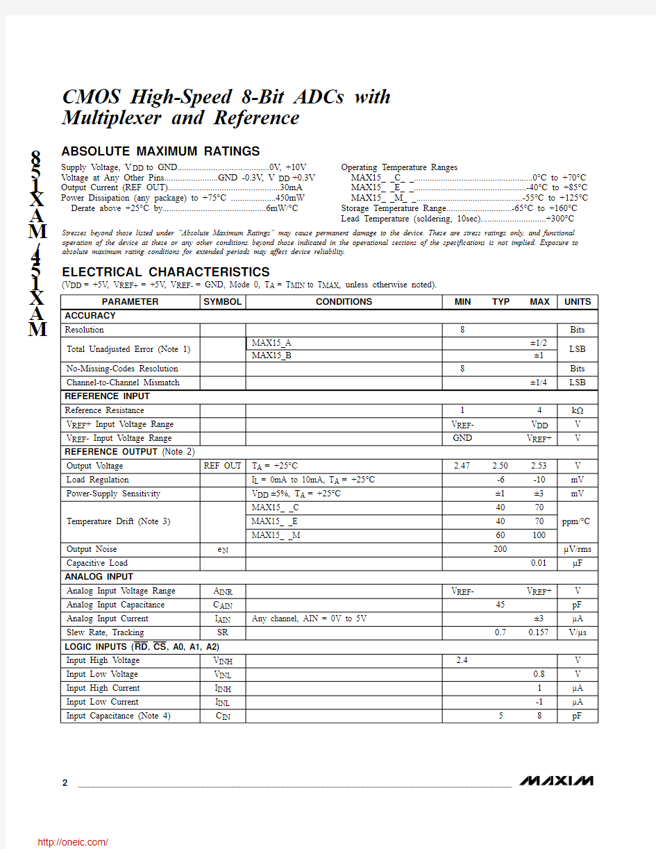
ABSOLUTE MAXIMUM RATINGS
ELECTRICAL CHARACTERISTICS
(V DD = +5V, V REF+= +5V, V REF-= GND, Mode 0, T A = T MIN to T MAX , unless otherwise noted).
Stresses beyond those listed under “Absolute Maximum Ratings” may cause permanent damage to the device. These are stress ratings only, and functional operation of the device at these or any other conditions beyond those indicated in the operational sections of the specifications is not implied. Exposure to absolute maximum rating conditions for extended periods may affect device reliability.
Supply Voltage, V DD to GND.........................................0V, +10V Voltage at Any Other Pins........................GND -0.3V, V DD +0.3V Output Current (REF OUT)..................................................30mA Power Dissipation (any package) to +75°C ....................450mW Derate above +25°C by..............................................6mW/°C
Operating Temperature Ranges
MAX15_ _C_ _.....................................................0°C to +70°C MAX15_ _E_ _..................................................-40°C to +85°C MAX15_ _M_ _...............................................-55°C to +125°C Storage Temperature Range.............................-65°C to +160°C Lead Temperature (soldering, 10sec).............................+300°C
ELECTRICAL CHARACTERISTICS (continued)
(V DD = +5V, V REF+= +5V, V REF-= GND, MODE 0, T A = T MIN to T MAX , unless otherwise noted).
TIMING CHARACTERISTICS (Note 5)
(V DD = +5V, V REF+= +5V, V REF-= GND, MODE 0, T A = T MIN to T MAX , unless otherwise noted).
Note 5:All input control signals are specified with t R = t F = 20ns (10% to 90% of +5V) and timed from a 1.6V voltage level.Note 6:Measured with load circuits of Figure 1 and defined as the time required for an output to cross 0.8V or 2.4V.Note 7:Defined as the time required for the data lines to change 0.5V when loaded with the circuits of Figure 2.
MAX154/MAX158
CMOS High-Speed 8-Bit ADCs with
Multiplexer and Reference
_______________________________________________________________________________________3
Note 1:Total unadjusted error includes offset, full-scale, and linearity errors.Note 2:Specified with no external load unless otherwise noted.
Note 3:Temperature drift is defined as change in output voltage from +25°C to T MIN or T MAX divided by (25 - T MIN ) or (T MAX - 25).Note 4:
Guaranteed by design.
M A X 154/M A X 158
CMOS High-Speed 8-Bit ADCs with Multiplexer and Reference 4
_______________________________________________________________________________________
__________________________________________Typical Operating Characteristics
(T A = +25°C, unless otherwise noted.)
2.5202.480
-50
150
REFERENCE TEMPERATURE DRIFT
2.490
2.510
M X 7824/28-1
AMBIENT TEMPERATURE (°C)
R E F O U T V O L T A G E (V )
2.500100
50
20
0-100
150
OUTPUT CURRENT vs. TEMPERATURE
4
12
16
AMBIENT TEMPERATURE (°C)
O U T P U T C U R R E N T (m A )
8100
-50
50
2.0
0300
900
ACCURACY
vs. DELAY BETWEEN CONVERSIONS (t p )
0.5
1.0
1.5
t p (ns)
L I N E A R I T Y E R R O R (L S B )
700
800
400
500
6002.0
5
ACCURACY vs. V REF
[V REF = V REF (+) - V REF (-)]
0.5
1.0
1.5
V REF (V)
L I N E A R I T Y E R R O R (L S B )
3
4
1
2
82
-100
150
POWER-SUPPLY CURRENT vs. TEMPERATURE
(NOT INCLUDING REFERENCE LADDER)
34567
AMBIENT TEMPERATURE (°C)
I D D – S U P P L Y C U R R E N T (m A )
50
100
-50
Figure 1. Load Circuits for Data-Access Time Test Figure 2. Load Circuits for Data-Hold Time Test
MAX154/MAX158
CMOS High-Speed 8-Bit ADCs with
Multiplexer and Reference
_______________________________________________________________________________________
5
_____________________________________________________________Pin Descriptions
M A X 154/M A X 158
CMOS High-Speed 8-Bit ADCs with Multiplexer and Reference 6
_______________________________________________________________________________________
_______________Detailed Description
Converter Operations
The MAX154/MAX158 use what is commonly called a "half-flash" conversion technique (Figure 3). Two 4-bit flash ADC converter sections are used to achieve an 8-bit result. Using 15 comparators, the upper 4-bit MS (most significant) flash ADC compares the unknown input voltage to the reference ladder and provides the upper four data bits.
An internal DAC uses the MS bits to generate an analog signal from the first flash conversion. A residue voltage representing the difference between the unknown input and the DAC voltage is then compared to the reference ladder by 15 LS (least significant) flash comparators to obtain the lower four output bits.
Operating Sequence
The operating sequence is shown in Figure 4. A conver-sion is initiated by a falling edge of RD and CS. The comparator inputs track the analog input voltage for approximately 1μs. After this first cycle, the MS flash result is latched into the output buffers and the LS con-goes low approximately 600ns later,indicating the end of the conversion, and that the lower four bits are latched into the output buffers. The data can then be accessed using the CS and RD inputs.
___________________Digital Interface
The MAX154/MAX158 use only Chip Select (CS) and Read (RD) as control inputs. A READ operation, taking CS and RD low, latches the multiplexer address inputs and starts a conversion (Table 1).
There are two interface modes, which are determined by the length of the RD input. Mode 0, implemented by keeping RD low until the conversion ends, is designed for microprocessors that can be forced into a WAIT state. In this mode, a conversion is started with a READ low), and data is read when the conversion ends. Mode 1, on the other hand,does not require microprocessor WAIT states. A READ operation simultaneously initiates a conversion and reads the previous conversion result.
Figure 3. Functional Diagram
Figure 5 shows the timing diagram for Mode 0 opera-tion. This is used with microprocessors that have WAIT state capability, whereby a READ instruction is extend-ed to accommodate slow-memory devices. Taking CS and RD low latches the analog multiplexer address and starts a conversion. Data outputs DB0–DB7 remain in the high-impedance condition until the conversion is complete.
(RDY). RDY, an open-drain output (no internal pull-up
device), is connected to the processor’s READY/WAIT input. RDY goes low on the falling edge of CS and goes high impedance at the end of the conversion, when the conversion result appears on the data outputs. If the RDY output is not required, its external pull-up resistor can be omitted. INT goes low when the conversion is complete and returns high on the rising edge of CS or RD.
Interface Mode 1
Mode 1 is designed for applications where the micro-processor is not forced into a WAIT state. Taking CS low latches the multiplexer address and starts a conversion (Figure 6). Data from the previous conversion is immediately read from the outputs (DB0–DB7).
INT goes high at the rising edge of CS or RD and goes low at the end of the conversion. A second READ oper-ation is required to read the result of this conversion.The second READ latches a new multiplexer address and starts another conversion. A delay of 2.5μs must be allowed between READ operations. RDY goes low on the falling edge of CS and goes high impedance at the rising edge of CS. If RDY is not needed, its external pull-up resistor can be omitted.
MAX154/MAX158
CMOS High-Speed 8-Bit ADCs with
Multiplexer and Reference
_______________________________________________________________________________________7
Figure 5. Mode 0 Timing Diagram
M A X 154/M A X 158
_____________Analog Considerations
Reference and Input
The V REF + and V REF - inputs of the converter define the zero and the full-scale of the ADC. In other words, the voltage at V REF - is equal to the input voltage that pro-duces an output code of all zeros, and the voltage at V REF + is equal to input voltage that produces an output code of all ones (Figure 7).
Figure 8 shows some possible reference configura-tions. A 0.01μF bypass capacitor to GND should be used to reduce the high-frequency output impedance of the internal reference. Larger capacitors should not be used, as this degrades the stability of the reference buffer. The 2.5V reference output is with respect to the GND pin.
Bypassing
A 47μF electrolytic and 0.1μF ceramic capacitor should be used to bypass the V DD pin to GND. These capaci-tors must have minimum lead length, since excess lead length may contribute to conversion errors and insta- bility. If the reference inputs are driven by long lines,they should be bypassed to GND with 0.1μF capac-itors at the reference input pins.
CMOS High-Speed 8-Bit ADCs with Multiplexer and Reference 8
_______________________________________________________________________________________
Figure 6. Mode 1 Timing Diagram
Input Current
The converters’ analog inputs behave somewhat differ-ently from conventional ADCs. The sampled data com-parators take varying amounts of current from the input,depending on the cycle they are in. The equivalent cir-cuit of the converter is shown in Figure 9a. When the conversion starts, AIN(n) is connected to the MS and LS comparators. Thus, AIN(n) is connected to thirty-one 1pF capacitors.
To acquire the input signal in approximately 1μs, the input capacitors must charge to the input voltage through the on-resistance of the multiplexer (about 600?) and the comparator’s analog switches (2k ?to 5k ?per compara-tor). In addition, about 12pF of stray capacitance must be charged. The input can be modeled as an equivalent RC network shown in Figure 9b. As R S (source impedance)increases, the capacitors take longer to charge.
Since the length of the input acquisition time is internal-ly set, large source resistances (greater than 100?) will cause settling errors. The output impedance of an op-amp is its open-loop output impedance divided by the loop gain at the frequency of interest. It is important that the amplifier driving the converter input have suffi-cient loop gain at approximately 1MHz to maintain low output impedance.
Input Filtering
The transients in the analog input caused by the sam-pled data comparators do not degrade the converter’s performance, since the ADC does not “look” at the input when these transients occur. The comparator’s outputs track the input during the first 1μs of the con-version, and are then latched. Therefore, at least 1μs will be provided to charge the ADC’s input capaci-tance. It is not necessary to filter these transients with an external capacitor on the AIN terminals.
Sinusoidal Inputs
The MAX154/MAX158 can measure input signals with slew rates as high as 157mV/μs to the rated specifications.This means that the analog input frequency can be as high as 10kHz without the aid of an external track/hold.The maximum sampling rate is limited by the conversion time (typical t CRD = 2μs) plus the time required between conversions (t p = 500ns). It is calculated as:
f MAX = 1 = 1 =400kHz
t CRD + t p (2.0 + 0.5) μs f MAX permits a maximum sampling rate of 50kHz per
channel when using the MAX158 and 100kHz per channel when using the MAX154. These rates are well above the Nyquist requirement of 20kHz sampling rate for a 10kHz input bandwidth.
MAX154/MAX158
CMOS High-Speed 8-Bit ADCs with
Multiplexer and Reference
_______________________________________________________________________________________
9
Figure 8a. Internal Reference
Figure 8b. Power Supply as Reference
Figure 8c. Inputs Not Referenced to GND
M A X 154/M A X 158
Bipolar Input Operation
The circuit in Figure 10a can be used for bipolar input operation. The input voltage is scaled by an amplifier so that only positive voltages appear at the ADC’s inputs. The analog input range is ±4V and the output code is complementary offset binary. The ideal input/output characteristic is shown in Figure 10b.
CMOS High-Speed 8-Bit ADCs with Multiplexer and Reference 10
______________________________________________________________________________________
Figure 9a. Equivalent Input Circuit
Figure 10b. Transfer Function for ±4V Input Operation
Figure 11. Simple Mode 0 Interface
Figure 9b. RC Network Model
Figure 10a. Bipolar ±4V Input Operation
分销商库存信息:
MAXIM
MAX154BCNG+MAX154ACWG+MAX158ACAI+ MAX158AEAI+MAX154BCAG+T MAX154BCWG+T MAX158BCWI+T MAX158BCAI+T MAX154BEWG+T MAX154ACWG+T MAX158BEWI+T MAX158ACWI+T MAX158BEAI+T MAX154BCAG+MAX158ACAI+T MAX158BCWI+MAX158BCAI+MAX154AEWG+T MAX158AEAI+T MAX154BEWG+MAX154BCWG+ MAX158BEWI+MAX158ACWI+MAX158BEAI+ MAX158BCPI+MAX154AEWG+MAX154BENG+ MAX154ACNG+MAX158BEPI+MAX158ACPI+ MAX154AENG+