CD4025C中文资料
TL F 5955CD4023M CD4023C Triple 3-Input NAND Gate CD4025M CD4025C Triple 3-Input NOR Gate
February 1988
CD4023M CD4023C Triple 3-Input NAND Gate CD4025M CD4025C Triple 3-Input NOR Gate
General Description
These triple gates are monolithic complementary MOS (CMOS)integrated circuits constructed with N-and P-chan-nel enhancement mode transistors All inputs are protected against static discharge with diodes to V DD and V SS
Features
Y Wide supply voltage range 3 0V to 15V Y High noise immunity
0 45V DD (typ )
Y 5V–10V parametric ratings Y
Low power
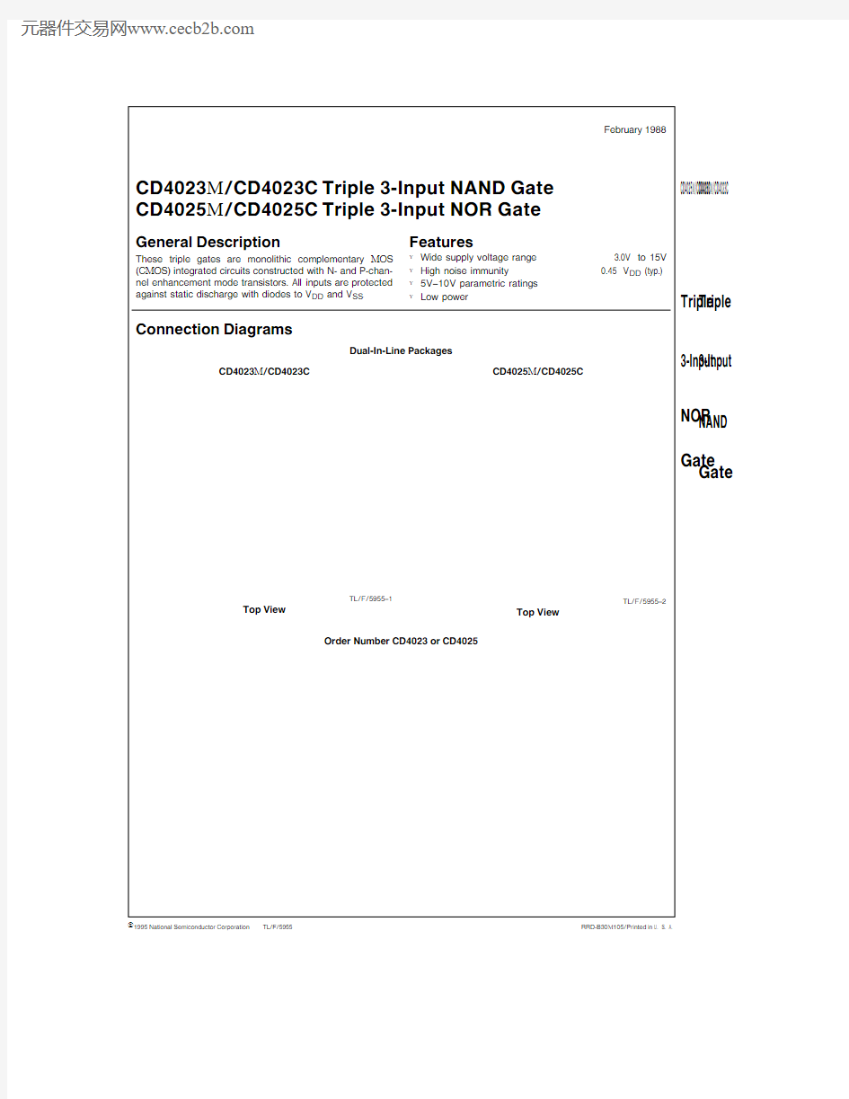
Connection Diagrams
Dual-In-Line Packages
CD4023M CD4023C
TL F 5955–1
Top View
CD4025M CD4025C
TL F 5955–2
Top View
Order Number CD4023or CD4025
C 1995National Semiconductor Corporation RRD-B30M105 Printed in U S A
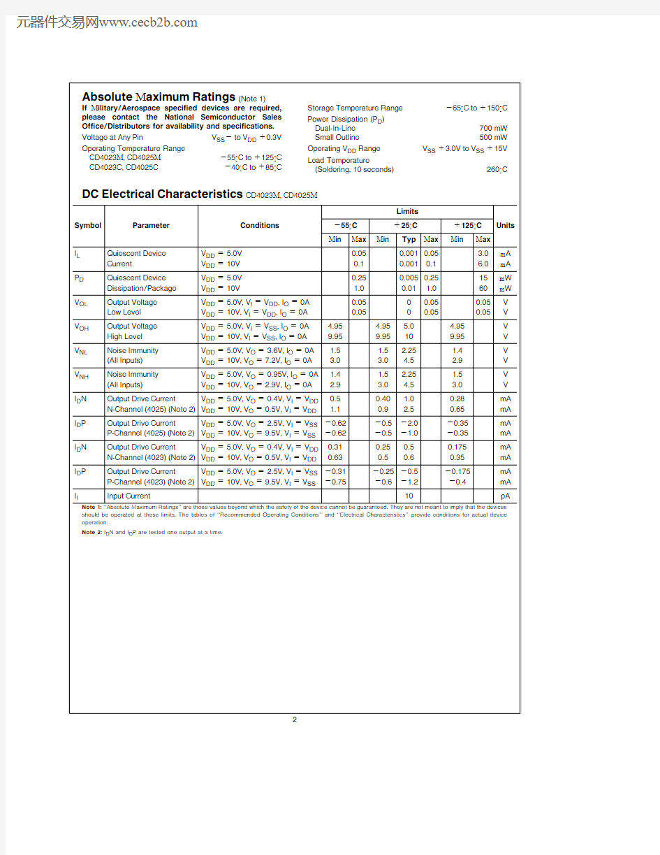
Absolute Maximum Ratings(Note1)
If Military Aerospace specified devices are required please contact the National Semiconductor Sales Office Distributors for availability and specifications Voltage at Any Pin V SS b to V DD a0 3V Operating Temperature Range
CD4023M CD4025M b55 C to a125 C CD4023C CD4025C b40 C to a85 C Storage Temperature Range b65 C to a150 C Power Dissipation(P D)
Dual-In-Line700mW Small Outline500mW Operating V DD Range V SS a3 0V to V SS a15V Lead Temperature
(Soldering 10seconds)260 C
DC Electrical Characteristics CD4023M CD4025M
Limits
Symbol Parameter Conditions b55 C a25 C a125 C Units
Min Max Min Typ Max Min Max
I L Quiescent Device V DD e5 0V0 050 0010 053 0m A
Current V DD e10V0 10 0010 16 0m A
P D Quiescent Device V DD e5 0V0 250 0050 2515m W Dissipation Package V DD e10V1 00 011 060m W
V OL Output Voltage V DD e5 0V V I e V DD I O e0A0 0500 050 05V Low Level V DD e10V V I e V DD I O e0A0 0500 050 05V
V OH Output Voltage V DD e5 0V V I e V SS I O e0A4 954 955 04 95V High Level V DD e10V V I e V SS I O e0A9 959 95109 95V
V NL Noise Immunity V DD e5 0V V O e3 6V I O e0A1 51 52 251 4V (All Inputs)V DD e10V V O e7 2V I O e0A3 03 04 52 9V
V NH Noise Immunity V DD e5 0V V O e0 95V I O e0A1 41 52 251 5V (All Inputs)V DD e10V V O e2 9V I O e0A2 93 04 53 0V
I D N Output Drive Current V DD e5 0V V O e0 4V V I e V DD0 50 401 00 28mA
N-Channel(4025)(Note2)V DD e10V V O e0 5V V I e V DD1 10 92 50 65mA
I D P Output Drive Current V DD e5 0V V O e2 5V V I e V SS b0 62b0 5b2 0b0 35mA
P-Channel(4025)(Note2)V DD e10V V O e9 5V V I e V SS b0 62b0 5b1 0b0 35mA
I D N Output Drive Current V DD e5 0V V O e0 4V V I e V DD0 310 250 50 175mA
N-Channel(4023)(Note2)V DD e10V V O e0 5V V I e V DD0 630 50 60 35mA
I D P Output Drive Current V DD e5 0V V O e2 5V V I e V SS b0 31b0 25b0 5b0 175mA
P-Channel(4023)(Note2)V DD e10V V O e9 5V V I e V SS b0 75b0 6b1 2b0 4mA
I I Input Current10pA
Note1 ‘‘Absolute Maximum Ratings’’are those values beyond which the safety of the device cannot be guaranteed They are not meant to imply that the devices should be operated at these limits The tables of‘‘Recommended Operating Conditions’’and‘‘Electrical Characteristics’’provide conditions for actual device operation
Note2 I D N and I D P are tested one output at a time
2
DC Electrical Characteristics CD4023C CD4025C
Limits
Symbol Parameter Conditions b40 C a25 C a85 C Units
Min Max Min Typ Max Min Max
I L Quiescent Device V DD e5 0V0 050 0050 515m A
Current V DD e10V5 00 0055 030m A
P D Quiescent Device V DD e5 0V2 50 0252 575m W Dissipation Package V DD e10V500 0550300m W
V OL Output Voltage V DD e5 0V V I e V DD I O e0A0 0100 010 05V Low Level V DD e10V V I e V DD I O e0A0 0100 010 05V
V OH Output Voltage V DD e5 0V V I e V SS I O e0A4 994 995 04 95V High Level V DD e10V V I e V SS I O e0A9 999 99109 95V
I I Input Current10pA
V NL Noise Immunity V DD e5 0V V O e3 6V I O e0A1 51 52 251 4V (All Inputs)V DD e10V V O e7 2V I O e0A3 03 04 52 9V
V NH Noise Immunity V DD e5 0V V O e0 95V I O e0A1 41 52 251 5V (All Inputs)V DD e10V V O e2 9V I O e0A2 93 04 53 0V
I D N Output Drive Current V DD e5 0V V O e0 4V V I e V DD0 350 31 00 24mA
N-Channel(4025)(Note2)V DD e10V V O e0 5V V I e V DD0 720 62 50 48mA
I D P Output Drive Current V DD e5 0V V O e2 5V V I e V SS b0 35b0 3b2 0b0 24mA
P-Channel(4025)(Note2)V DD e10V V O e9 5V V I e V SS b0 3b0 25b1 0b0 2mA
I D N Output Drive Current V DD e5 0V V O e0 4V V I e V DD0 1450 120 50 095mA
N-Channel(4023)(Note2)V DD e10V V O e0 5V V I e V DD0 30 250 60 2mA
I D P Output Drive Current V DD e5 0V V O e2 5V V I e V SS b0 145b0 12b0 5b0 095mA
P-Channel(4023)(Note2)V DD e10V V O e9 5V V I e V SS b0 35b0 3b1 2b0 24mA
I I Input Current10pA
Note1 ‘‘Absolute Maximum Ratings’’are those values beyond which the safety of the device cannot be guaranteed They are not meant to imply that the devices should be operated at these limits The tables of‘‘Recommended Operating Conditions’’and‘‘Electrical Characteristics’’provide conditions for actual device operation
Note2 I D N and I D P are tested one output at a time
3
AC Electrical Characteristics T A e25 C C L e15pF and input rise and fall times e20ns Typical temperature coefficient for all values of V DD e0 3% C
Symbol Parameter Conditions Min Typ Max Units
CD4025M
t PHL Propagation Delay Time V DD e5 0V3550ns High to Low Level V DD e10V2540ns
t PLH Propagation Delay Time V DD e5 0V3540ns Low to High Level V DD e10V2570ns
t THL Transition Time V DD e5 0V65125ns High to Low Level V DD e10V3570ns
t TLH Transition Time V DD e5 0V65175ns Low to High Level V DD e10V3575ns
C I Input Capacitance Any Input5 0pF
CD4025C
t PHL Propagation Delay Time V DD e5 0V3580ns High to Low Level V DD e10V2555ns
t PLH Propagation Delay Time V DD e5 0V35120ns Low to High Level V DD e10V2565ns
t THL Transition Time V DD e5 0V65200ns High to Low Level V DD e10V35115ns
t TLH Transition Time V DD e5 0V65300ns Low to High Level V DD e10V35125ns
C I Input Capacitance Any Input5 0pF
CD4023M
t PHL Propagation Delay Time V DD e5 0V5075ns High to Low Level V DD e10V2540ns
t PLH Propagation Delay Time V DD e5 0V5075ns Low to High Level V DD e10V2540ns
t THL Transition Time V DD e5 0V75125ns High to Low Level V DD e10V5075ns
t TLH Transition Time V DD e5 0V75100ns Low to High Level V DD e10V4060ns
C I Input Capacitance Any Input5 0pF
CD4023C
t PHL Propagation Delay Time V DD e5 0V50100ns High to Low Level V DD e10V2550ns
t PLH Propagation Delay Time V DD e5 0V50100ns Low to High Level V DD e10V2550ns
t THL Transition Time V DD e5 0V75150ns High to Low Level V DD e10V50100ns
t TLH Transition Time V DD e5 0V75125ns Low to High Level V DD e10V4075ns
C I Input Capacitance Any Input5 0pF AC Parameters are guaranteed by DC correlated testing
4
Physical Dimensions inches(millimeters)
Ceramic Dual-In-Line Package(J)
Order Number CD4023MJ CD4023CJ CD4025MJ or CD4025CJ
NS Package Number J14A
5
C D 4023M C D 4023C T r i p l e 3-I n p u t N A N D G a t e C D 4025M C D 4025C T r i p l e 3-I n p u t N O R G a t e
Physical Dimensions inches (millimeters)(Continued)
Molded Dual-In-Line Package (N)
Order Number CD4023MN CD4023CN CD4025MN or CD4025CN
NS Package Number N14A
LIFE SUPPORT POLICY
NATIONAL’S PRODUCTS ARE NOT AUTHORIZED FOR USE AS CRITICAL COMPONENTS IN LIFE SUPPORT DEVICES OR SYSTEMS WITHOUT THE EXPRESS WRITTEN APPROVAL OF THE PRESIDENT OF NATIONAL SEMICONDUCTOR CORPORATION As used herein 1 Life support devices or systems are devices or 2 A critical component is any component of a life systems which (a)are intended for surgical implant support device or system whose failure to perform can into the body or (b)support or sustain life and whose be reasonably expected to cause the failure of the life failure to perform when properly used in accordance support device or system or to affect its safety or with instructions for use provided in the labeling can effectiveness
be reasonably expected to result in a significant injury to the user
National Semiconductor National Semiconductor National Semiconductor National Semiconductor Corporation
Europe
Hong Kong Ltd
Japan Ltd
1111West Bardin Road
Fax (a 49)0-180-5308586
13th Floor Straight Block Tel 81-043-299-2309